Note: Descriptions are shown in the official language in which they were submitted.
~ 3 2 ~ ~r3 ll 3 20365-2990
_CKGROUND CF ~IL~ r~.-
Field of the Invention
This invention relates to a process for the reception
of a binary digital signal, which may also exhibit phase shifts,
and it relates, more par-ticularly, to an arrangement including
elements having an appro~imately constant propagation delay,
operating at a clock whose frequency is equal to or plesiochronous
with the bit rate of the digital signal and whose phase difference
is selected arbitrarily with respect to the digital signal.
BRIEF DESCRIPTION OF T~IE DRAWINGS
Figure 1 provides an explanation of jitter.
Figure 2 shows a moment at which a pulse is received.
Figure 3 shows a basic circuit diagram of an illus-
trative embodiment for carrying out the process according to the
invention for cons-tant delays.
Figure 4 provides a basic circuit diagram of an illus-
trative embodiment for carrying out -the process according to the
invention for fluctuating delays.
Figure 5 depicts a circuit diagram of an actual
illustrative arrangement in accordance with Figure 4.
Figure 6 shows a circuit diagram of a practical illus-
trative embodiment in accordance with Figure 3.
Description of the Prior Art
A circuit arrangement for the regeneration and syn-
chronization of a digital signal, which compensates for the phase
oscillations of the incoming signal bits, is already known from
- 2 -
~ 3 2 Q .~ 20365-2990
German patent document DE 34 31 501 Al. For that purpose, it
contains a series circuit consisting of a controllable delay line
coupled to a delay control unit, to which the controllable delay
line is connected through address lines. The decision logic is
supplied over a clock line with a system clock whose frequency
corresponds to the bit rate of the digital signal that is to be
regenerated and synchronized.
In an ideal binary digital signal, the rising and
falling edges of each binary digit lie within a fixed pattern,
which is determined by the period of the clock frequency. Any
deviation of the edges from this pattern is referred to as
jitter. Within defined limits, this jitter must not result in
information errors when the signal is received.
Two different kinds of jitter can be distinguished.
The first consists of time deviations of two successive edges
from the
- 2a -
.~
11 3 2 ~ 3
prescribed raster, the second of slowly developing phase shifts,
which can lead to a time shift of more than one period.
Fig. 1 shows a period T of th~ clock frequency, with a
permissible jitter range -x and +x for the pulse transitions or
edges. For a delay-free phase equalization, only one edge can be
the reference point for the arrival of a new pulse of the digital
signal. If this occurs, in accordance with Fig. 2, at the time t2,
then a half-period T/2 of the clock ~requency must elapse before the
pulse is received at time t4. The deviations that can occur in the
determination of the time T/2 are taken into account by the time
intervals + Ay and --y.
If the edge arrives at time t3, then reception is possible only
15 when
T/2 + ~y < T - 2x. (1)
On the other hand, if the edge arrives at time tl, then perfect
reception requires that
T/2 - y > 2x. ~2)
SUMMARY OF THE INVENTION
An object of the present inventlon is to provide a process for
the inertia-free reception of a binary digital signal with a
changing phase position.
Using a process of the type described in the introduction as
a basis, the invention accomplishes the foregoing purpose by a
process step set wherein a binary digital signal subject to phase
shifts.
An edge that serves to derive pulses is also referred to as an
effective edge.
~2~13
The deviation ~y depends first of all on the basic or
additional delay ~tl, which can be expressed as the time interval
T/n, where n is the number n of the pulses. It is also dependent
on the accuracy ~ with which the time interval T/2 can be measured.
This can be accomplished over a fixed number of gate delays. The
~ormula for the deviation is then
~y = T/n - S - T~2 (3)
By combining (1), (2) and (3), we obtain:
x = T n(1 ~ 2 (4)
4n
The process according to the invention can be used in
synchronously operating systems. In this case a perfect reception
of the data signals is made possible by the compensation of any
desired phase position. This process has the effect of clock
recovery.
Another possible application is a block switching, in which a
synchronization of the block frequencies is unnecessary. The
process can be used in order to compensate a phase that is
continually changing because of differences in the clock frequency.
However, it can also be used when the! various information blocks
have different phase positions.
If this process is to be carried out in an integraked circuit
in which, due to sample dispersions and operating tolerances, the
basic or additional delays and the delays in all the other elements
lie within a defined range, there must be a compensation of the
change in the delay of the elements, so that the effective edge of
the input clock is delayed by about half a clock period T/2 with
respect to the effective edge of the digital signal.
0365-2990
According to a broad aspect of the invention there is
provided a process for receiving a binary digital signal, which
may also have phase shifts, using a clock signal, whose frequency
is plesiochronous wi-th or equal to the bit rate of the digital
signal and whose phase difference is selected arbitrarily with
respect to the digital signal, the process comprising the steps
of: applying the clock si.gnal -to serially connected delay elements
with approximately constant delays; deriving a series of n + p + 1
clock pulses from the clock signal, through transmission over n
principal ones of said delay elements with appro~imately equal
principal delays and a total principal delay of at least one clock
period and over p additional ones of said delay elements with
additional delays equal to the principal delays ~tl), where n is
an integer greater than three and p is an integer greater than
or equal to ~ero; deriving a sequence of shorter pulses from the
rising and/or falling edges of the clock pulses, each of said
shorter pulses having a duration that is greater than a principal
delay and, given large values of n, is big enough so that logic
elements can be driven by said shorter pulses which are short with
respect to the clock period; deriving read pulses and reset pulses
from the rising and/or falling edges of the digital signal, with
a duration that is small compared with a clock period, but large
enough so that logic elements can be driven by said read pulses
and said reset pulses; storing in memory elements during the
occurrence of a read pulse a simultaneously occurring shorter
pulse or pulses of the sequence of shorter pulses, after the
-- 5 ~
~32~3 20365-2990
memory elements have been cleared immediately before with the
resetting pulses; switching through a clock for every memory
elemen~ that has stored a pulse o~ the sequence of shorter pulses,
which originates from a delay element that is downstream of the
delay element from whose clock the stored pulse was derived;
blocking a clock from every memory element that has not stored
a pulse; OR-linking the clocks that have been switched through
and blocked to form an OR-linked input clock; selecting the clock
or clocks that has/have been switched through from the principal
and additional delay elements that are connected downstream in
each case in such a manner that the rising and/or falling edge of
the OR--linked input clock formed from the clocks that have been
switched through and blocked arrives delayed by about half a clock
period with respect to the edge of the digital signal; and reading
the digital signal as an output digital signal responsive to the
rising or falling edge of the input clock.
Features of the invention and additional objects of the
invention will be more readily appreciated and better understood
by reference to the following detailed description which should
be considered in conjunction with the drawings.
DETAII.ED DESCRIPTION
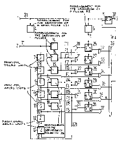
Figure 3 shows a basic diagram of an arrangementfor the
implementation of the process with constant delays. The arrange-
ment includes a D flip-flop 6, an arrangement 4 for the deriva-
tion of a short read pulse I21 and an arrangement 5 for the
derivation of a reset pulse RI from the effecti~e edge of a
~ 2036~-2990
digital signal Dl, principal delay units "G" 7 - ll, additional
delay units "2l 12 and 13, arrangements 14 - l9 for the deriva-
tion of the pulses Ill - I16, AND gates 20 - 25 and 32 - 37,
SR flip-flops 26 - 31 and an OR gate 380 The arrangements 4 and
5, and 14 - 19 may be implemented by a circuit such as that
labelled "B" in Figure 5.
An input 2 receives a clock frequency Tl which may
deviate slightly from the bit sequence frequency of a digital
signal Dl at the input 1 and may have an arbitrary phase position
with respect to it.
The digital signal Dl is fed to the D input of the D
flip-flop 6. The rising edges of the digital signal Dl are the
effective edges. In the arrangement 4, read pulses I21 are derived
from these edges. The duration of these pulses is small compared
to a clock period T, but large enough so that logic elements can
be driven by them. In the arrangement 5 further reset pulses RI
of corresponding duration are derivecl from the effective edges of
the digital signal Dl and fed to the R inputs of all the ~R flip-
flops 26 - 31. The clock signal T1 is fed into the delay line of
elements 7 - 13, which comprises principal delay elements "G"
7 - ll, and additional delay units "Z" 12 and 13. The principal
and additional delays ~tl are equal to T/6. Each principal delay
unit "G" drives from the effective edges of the clock signals Tl
to T6 short pulses Ill to Il6, whose duration is larger than the
principal delay Qtl and is large enough, even for big values of n,
so that logic elements can be driven by them. The pulses Ill -
-20365-2990
~329~3
Il6 are each applied to one input of the AND gates 20 - 25. The
second inputs are connected with -the outpu-t of the arrangement 4.
When a read pulse I21 arrives from this output, then the pulse or
pulses that are already present is/are switched through from
the sequence Ill - Il6 and arrive at the setting input S of the
S~ flip-flops 26 - 31, which have been
- 7a. -
~ 3 ~
reset with a reset:ting pulse shortly before. The Q outputs o~ these
RS flip-flops 26 - 31 are connected to the first inputs of the AND
gates 32 - 37, whose second inputs are connected with clock outputs
of the principal delay units "&" 8 - 11 and the additional delay
units "Z" 12 and 13. The pulses T3 - T8 have been renamed F1 - F6
for further processing. The outputs of the AND gates 32 - 37 are
wired to the inputs of the OR gate 38 and its output is wired in
turn to the clock input of the D flip-flop 6.
All the elements in this arrangement have propagation delays.
Due to the time interval between the arrival of the signals at the
two inputs of the AND gates 32 ~ 37, the delay between the effective
edge of the digital signal Dl and that of the input clock Te at the
clock input of the D flip-flop 6 can be set in such a manner that
it is equal to T/2 for each newly received pulse of the digital
signal D1. The emitted digital signal D2 thus consists only of
correctly scanned pulses.
Fig. 4 shows a basic diagram of an arrangement for the
implementation of the process with fluctuating delays. The
arrangement comprises all the elements of the arrangement according
to Fig. 3. In addition, it includes auxiliary delay units "H" 39
- 41, arrangements 42 - 45 for the derivation of read pulses I21 -
I24, a clock period measurement device 46, AND gates 47 - 50, 60 -
63 and 68 - 71, supplementary delay units "E" 52 - 55, arrangements
56 - 59 for the derivation of pulsas I17 - I110, SR flip-flops 64
- 67 and an OR gate 51.
For the maximum delay tl, the principal delay units "G" are
sufficient. For the minimum delay, the number of supplementary
delay lines "E" must be chosen in such a manner that a further
delay, equal to a clock period T takes place along the delay units
of these two kinds.
~ ~ 2 ~ ~ ~ 3 20365-2990
Since, in spite of the fluctuating delay, the delay
between the effective edge of the digital signal Dl and that of
the input clock Te is to be equal to half a clock period T/2, an
adjustable delay of the read command is introduced in the
signal processing path. This is achieved by a gradual delay of
the digital signal Dl so that a sequence of read pulses I21 -
I24 is derived over the auxiliary delay elements "H" 39 - 41
with auxiliary delays ~t2 and the arrangements 42 - 45.
When a pulse Ill has been derived in the arrangement
14, the clock period measurement device 46 determines which of
the arrangements 56 - 59 has a pulse at its output at that time.
According to the result in each case, either a read pulse I21 is
switched through over the AND gate 47, or a read pulse I22, I23
or I24 which is delayed with respect to the read pulse I21 is
switched through one of the AND gates 48 - 50, as a read pulse
I2x. This pulse then arrives through the OR gate 51 at the
second inputs of the AND gates 20 - 25 and 60 - 63. The process
then proceeds as has already Deen described with respect to
Figure 3. The arrangements 42 - 45 and 56 - 59 may be implemen-
ted by the circuit labelled "B" in Figure 5.
Figure 5 shows a practical arrangement using the basic
circuit diagram of Figure 4. The arrangement comprises a NAND
gate 72, non-inverting gate elements 73 - 90 and inverting gate
elements 91 - 99, each of which is used for time delay, AND
gates 100 - 115l D flip-flops "A" 116 - 124, an OR gate 125,
circuit complexes "B" 126 - 142, circuit complexes i'C" 143 - 157,
~ 20365-2990
an OR gate 158 and the D flip-flop 6.
The c.ircuit complex "B" eomprises an AND gate 159, an
inverting gate element 160 for delay and non-inverting gate
elements 161 and 162 for. delay. The lower terminal is connected
to the upper terminal (not shown) of the subse~uent circult
complex "B" 126. The cireuit complexes 126 - 142 are eonnected
with one another correspondingly.
- 9a -
~ 3 2 ~ ~ ~ 3
The circuit complex "c" comprises a NAND gate 163, an SR flip-
flop 164 and an AND gate 165.
In the D flip-flop "A" and the circuit complexes "B" and "C",
the terminals in the circuit diagram are arranged geometrically in
the same manner as in the "black boxes" 116 - 124, 126 - 142 and
143 - 157.
The circuit complexes "B" and "C" operate like the elements 7
- 37 and 52 - 71 in Fig. 4. The gates 73, 75, 77, 79, 81, 83, 85
and 87 form an auxiliary delay chain with eight members. The
non-inverting gates 74, 76, 78, 80, 82, 84, 86, 88 and 90 and the
inverting gates 91 - 99, when combined with the AND gates 100 - 108,
each produce with respect to its two left-hand inputs an arrangement
for the generation of a read pulse. In the D flip-flops '7A" 116 -
124, the pulse Ilx that is present in the circuit complexes "B" 132
- 140 at the time of a pulse I11 -- or two such pulses -- is stored
at a terminal X of a circuit complex "B".
Each of the AND gates ~00 - 108 which receives both a pulse
Ilx and a read pulse I2x emits a signal to the OR gate 125, at whose
output the read pulse I2x appears with the desired delay. The NAND
gate 72 supplies a reset pulse RI for all the SR flip~flops 164.
The AND gates 109 - 115 serve to suppress any second pulse Ilx
that may have been stored. If, for example, the Q outputs of the
D flip-flops "A" 116 and 117 are in the logic state "1", then the
logic state at the output of the AND gate 109 is also "l" and a
logic state "l" can occur at the output o~ the AND gate 102. Now
if a logic stat~ "0" occurs at the Q output of the D flip-flop "A",
then corresponding states must occur at the outputs of the AND gates
110 - 115.
132~3~3
Fig. 6 shows a practical embodiment of the arrangement
according to Fig. 3. The arrangement contains inverting gate
elements 166 - 169 and 172 - 187 for delay, exclusive OR gates 170
and 171 and 188 ~ 193/ AND gates 194 - 199 and 206 - 211, D flip-
flops 200 - 205, an OR gate 212 and the D flip-~lop 6 already shown
in Fig. 3.
~he digital signal D1 present at input 1 is read in the D flip-
flop 6 with the input pulse Te and received at the output 3 as a
digital signal D2.
The remainder of the circuit is used to derive the input pulse
Te from the clock Tl that is present at the input 2. For this
purpose, the clock signal T1 is fed into a delay chain 172 - 187
with sixteen members, in which every two inverting gate elements
form a delay element. Their number is chosen in such a manner that
the clock signal at the output of the inverting gate element 183 is
always delayed by one clock period with respect to the clock signal
T1 at the input 2, when the delay time per gate element is at a
minimum. The exclusive OR gates 188 - 193 emit pulses with a width
equal to three times the delay time of a gate element, if the state
of the delay chain 172 - 187 changes in its range. These pulses
cover, step by step, the phase range from 0 to 360.
The exclusive OR gate 170, in conjunction with the inverting
gate elements 166 and 167, emits a resetting pulse RI, which resets
all the D flip-flops 200 205 for each change in the state o~ the
digital signal Dl. As a result, all the Q outputs, the outputs o~
the AND gates 206 - 211 and the output of the OR gate 212 are in the
logic state "0".
The inverting gate elements 168 and 169 and the exclusive OR
gate 171 emit a read pulse that is delayed with resp~ct to the
resetting pulse ~I. From the AND gates 194 - 199, the exclusive OR
~ 3 2 ~ ~ ~ 3
gate receives at its output a logic state of "1", in which case the
same state occurs at the input of the respective delay element if
the read pulse is present. In addition, a loyic state of "1" must
be present at the output of the respective exclusive OR gate from
the exclusive OR gates 188 - 193 r which i5 true only when there is
a logic state of "0" at the output of the third inverting gate
element following the input of the delay element.
If the output of one or more of the AND gates 194 - 199
switches to the logic state "1", then the Q output of the next D
flip-flop of the D flip-flops 200 - 205 also receives the logic
state "1". The next ~ND gate of the AND gates 206 - 211 receives
at its output a logic state of "1", if not only the Q output of the
respective D flip-flop but also the Q output of the preceding D
flip-flop has the same state. In addition, khe logic state at the
output of the next delay element after that must have the loyic
state "1"~ The outputs of AND gates 206 ~ 211 will be linked at
OR gate 212. If two of the AND gates 206 - 211 have a logic state
"1" at the output, and are based on clock pulses which shift with
respect to each other by a c]ock period, that causes no problem.
There has thus been shown and described novel digital signal
receivers and their method of operation which fulfill all the
objects and advantages sought therefor. Many changes,
modifications, variations and other uses and applications of the
sub~ect invention will, however, becc,me apparent to those skilled
in the art after considering this specification and the accompanying
drawing which disclose the preferred embodiments thereof. All such
changes, modifications, variations and other uses and applications
which do not depart from the spirit and scope of the inv~ntion are
deemed to be covered by the invention which is limited only by the
claims which follow.
12