Note: Descriptions are shown in the official language in which they were submitted.
1 320746
COIN VALIDATOR
~ GRO~ND O~ TI~IE_INVENTION
1. Field of the Inven-tioll
This invention relates to coin validators usecl in
various automatic service devices of vencling mact~ es. etc.,
and more Particularly to such va:Lidators which dlscerll -the
thickness and/or Pattern of a coin in a non-contact manller.
2. DescriPtion of the Related Art
There is an electronic coin validator in whicll a
pair of electrodes are disPosed on -the corresponclincJ sicles of
a coin Path to detect the difference between the caPacitances
on the electrodes on s-tandbY and durillcJ coin passaCJe -to
thereby validate the coin.
More specificallYt as shown In Fi~J. 5, the
validator ircludes a Pail of oPposing electrodes 2 and 3
disposed so as to face the front and back of a coin I alonc3 a
coin path. an oscillator 4 which outputs an oscillatins
siclnal of a predetermined frequencY~ a resonator 7 including
a coil 5 and a capaci-tor 6 for aPplyins i-ts resonant output
across the electrodes 2 and 3. a buffer 8 for amplifying the
output signal from the resonator 7, a rectifYing and
smoothing circuit 9 for rectifYincJ and smoothincJ the signal
received via the buffer 8. an amplifier 10 for amplifYillcJ the
outPut skJnal from the rectifYing and smoothing Cil'CUi-t 9,
and a thickness/pattern detector 11 for detectillcl the
-thickness and Pattern of the coin I in accordance with a
1 320746
chall~Je in tl~e recti~iecl OUtPI.It si~Jnal via t~e n~ lifier 1
durillg the COi~ ass-lge an(l repoltin~J t.he resLIlt Or tlle
detec-tion to a contnollen 12 for colltrol of tl-e corrl~c)l~ ls o~
the validatol.
~ ccolclillcJ lo t}liS arran~Jelllellt~ a series resonator
of a resollallt frecluellc~ f0 = 1/2~ is constitllted l)Y the
oscillator 4 of an oscillatincJ frequencY fl coil 5 o~ L
Hellry and capacitor 6 of caPacitance of C Farad. inclllsive of
the caPacitance ~etweer the electrodes. The resonant
lo characteristic Or Fig. 6 is replesented bY a resollallt curve
shoon bY the ;olid line a on stanclbY wherein a vol.ta~Je vl is
cJenenated across the capacitoI 6.
Uncler such condition. whell a coin ~asses between
the electro~les 2 an(l 3 the caE~acltallce acnoss the eleotno(le;
2 an(l 3 chanc]es and the total caPaCitallce C chancJes. -the
resonallt frequellcY changes from f0 to foc and the resonant
cllalacteristic challses to the curve rePresented bY the broken
line b as shown in Fig. 6. Then the volta~e across the
capacitor 6 is attenuated from vl to vlc at a frequencY fl.
nalnelY~ the chanYe vl - vlc is senera-ted- The detector 11
uses this change to discern -the thickness and Pattern of -the
coin.
If in the conventional valida-tor the ind-lctance o.E
the coil 5 or the caPacitance of the caPaci tor 6 changes. for
example. due to a change in its ambient temPerature or if
components themselves vary from one manufacturing lot to
another the resonant frequency f0 chancJes for examPle. like
f0 in Fig. 6 a:nd the characteristic curve moves to the curve
1 320746
shown bY the dot dashed line c ancl thus the outPut voLIa(Je
vl from the caPaci-tor 6 on s-tandbY is attenuated to vl
Thus the difference be-tween the outPllt vlc obtained du~ J
the coin I Passase and the voltage vl is reclucecl to tilerel~Y
lose the stabilitY of -the validation ulldesirablY
l-t is an obiect of the Presellt inverltic)n to l~rovide
a coin validator which is caPable of discerllil1g the thicknes
or Pattern of a coin in a stabilizecd manner
~MARY OF TlIE IN~ENr ON
Accordincl to the Present invention there is
Provided a coin valida-tor comPriSincJ a COill sensol for
senslncJ a coin passing through a coin Path; al~ oscillator for
OUtpUttillg an oscillating si~nal of a precletermined
frequencY; a resonator resonant wi-th the oscillatincJ sic~nal
from the oscillator for applying a resonant outPut -to -the
coin sensor; a detec-tor for detec-tincJ the nature of the cc)in
in accordance with the outPut signal from the resonator
during coin passage; a variable capaci-tance diode adcled as a
resonant element to the resonator; and a resonant frequencY
control circui-t for res-tricting to within a Predetermined
range a change in the ou-tput signal from the resonator during
coin non-~assage by chansing a voltac~e aPplied across -the
variable caPaCitanCe diode
~ he present invention is characterized bY the
variable capacitance diode added as the resonant componellt -to
the resonator and the resonant frequency control circuit to
vary -the voltage applied across the diode to -thelebY suPPress
within a Predetermined range a fluctuation of the outPut
1 320746
sicJnal fronl the resonator duZil)c~ the tirne wl~en no COil~
Passes .
Whell the coin passes throu~h -the Path1 the coin
sensor senses it ancl the resollallt frequenc~7 in the resonator
chan~es. rhis causes the resonant outPut voltacJe to cha1lge
which follows a chancJe in -tl~e thickness or l~tterll of the
COill. The thicklless and pattern of the coin are cletected
witll the voltage corresPondillg to the cllallcJe or tlle wave~orm.
If the macJnitude of -the chan~Je in the resonant outPut voltacJe
signal is Wit]~ill a predeterlnined rallCJe of volta~Jes. -the COill
is validatecl to be in the Predeterrmilled ranCJe of tl~ic~llesses.
If the ~laveforln of the resonant output vol-taye siYn~l crosses
a Predeternlined voltacJe level bY a Precleternlinecl number of
times. -the tllickness of the coin is considerecl to fluctllate
in a Yiven thickness range and is cleterminecl to have a
pa-ttern~ .
If the resonant frequencY obtained on stanclby
deviates out of the reference resonant frequency range for
example due to a change in the ambient temPerature~ a
volta~e corresPonding to the clevia-tion is applied across the
variable caPaCitanCe diode and feedback control is Provlded
such that the resonant frequency falls within the reference
resonant frequencY range.
As Just described above~ according -to the presen-t
invention. unstablelless of Ol fluctuations in -the resonant
frequencY due to a chanYe in the ambien-t tempera-ture. etc
is eliminated to therebY allow -the thickness or Pattern of
-the coin to be discerned in a s-tabilizecl manner.
1 320746
BRIEE~ 5~UF~lQ _OF II-IE _FAWI_y~J-$-
Fi~J. I is a circuit diacJram of an embocliment o~ the
present invention;
Fig. 2 is a characteristic diacJram inclicative Or a
change in -the resonant frequencY;
Fig. 3 is a general charac-teris-lic diac~ram of a
variable caPacitance diode;
Fis. 4 is a charac-teristic diagram illus-tratins the
feedback control of the resonan-t frequencY;
FiY. 5 is a circui-t diagram of a conventional COill
validator: and
Fig. 6 Is a characteristic diagram illustrating a
change in the resonant frequencY in -the convel)tiolIal
validator.
_ESCRIPT,~ o~ o~Fw~3~bBoDl~iENT
Fig. I is a circuit diagram of one embocIimelIt of a
coin validator according to the present inven-tion. Like
parts or elements are identified by like reference numerals
in ~igs. 1 and 5 where Fig. 5 shows a prior validator, and
further description thereof will be omitted.
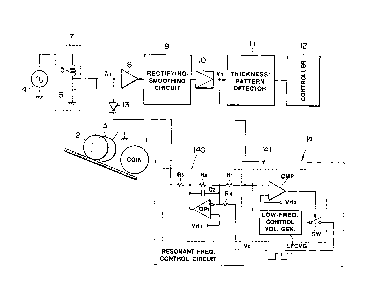
In ~i~. 1. a variable caPacitance diode 13 is newly
added as one of the resonator comPonents of a resonator 7
compared to -the validator of ~ig. 5. A con-troller 14 which
restricts fluctuations of the resonant frequencY in the
resonator 7 to wlthin a predetermined ran~e by aPPlyinc~ a
voltage across the diode 13 is newlY added as well.
The controller 14 inclucles a first control unit 140
which finelY adjusts fluc-tuations of -the resonant frequencY
1 320746
in a Predetermined control re~Jion, and a seconcl contro1 unit
141 which l~eturns the reso]lant charac-teristi(- into the
colltrol region when the resonant frequencY cleparts out of the
control region of the first control Ullit 140.
The first control uni-t 140 inclucles an operational
amplifier Pl. an integrating capacitor C2, ancl resis-lors Rl
- R4 witll a reference voltacJe Vrfl applied to one input
termillal of the amPlifier PI. An outPut voltaYe vl is
applied from the amPlifier 10 via the resistor Rl to tlle
other inPUt terminal of the a~nPlifier 0PI to which the
control voltage Vc is also applied from the secolltl colllrol
Ullit 141 via the resistor R4. Tlle outPut frorll the
operational amPlifler OPI is a~Plied across the diode 13 via
the resistol R3.
The seconcl control uni-t 141 incl-ldes a comParatol
CMP which compares the reference voltase Vrf2 with the outPut
voltage vl from the amPlifier 10 and tulns on a switch SW
when the vl ~ Vrf2, and a low-frequencY control volta~Je
cJenerator LFCVG which Provicles a control voltage Vc chancJing
at a low frequencY between the higl- and low levels via the
switch SW and to the inPut resistor R4 of -the oPerationa
amplifier Pl of the first control unit 1~0.
In the above arransement. the process for
valldating a coin is similar to that performed bY the prior
validator and further descriPtion thereof will be omitted.
Only the control of the resonant frequencY will be described
in detail below.
First. in Fig. 1. the oscillator 4 generates an
1 320746
oscillatincJ signal of a fre~luencY -fl. The resonant frecluer
Eo of the resonator 7 is siven bY
fO = 1/2~ L (C + CD)
where L is the inductance of lhe coil 5 (HellrY)~ Cv is the
capacitance of the diode 13, C is tl~e total of the stray
capacitance inherent -to the electrodes 2 and 3 and the
capacitance of the caPacitor 6 (Farads). The relatiollsllip
between fO and fl is fO ~ El, as shown in Fig. 2. Reterence
charac-ter vl ill Fig. 2 denotes a voltage across the capacitor
6 at fl of the resonant curve a represented by the solid
line.
For instance. if the inductance value L or
capacitance value C chanses, the resonant frequellcy fO
fluctuates. and the resollant culve a replesellted by the solicl
line in Fig. 2 moves leftward (toward a lower frequencY) or
rightward ttoward a hic~hel frequency). Namely, if L, C or CD
increases. the resonant curve a moves leflward in Fig. 2
while if L or CD decreases, the resonant curve a moves
rightward.
Assuming that the inductance of the coil 5
increases to L', the resonant frequencY changes from
fO = 1~2/~ L (C + C
to
-
fO = 1/2~ ~ (C -~ CD)
and the resonant curve moves from the curve a (solid line) to
the curve b (dot-dashed llne). As a result, the voltage
across the capacltor 6 is attenuated from vl to vl' in Fig.
2.
1 3207~h
It is meal~t by this fact tllat tlle oUtF~lt direct
currellt voltage fl`OIIl llle alllPl if lel 1O iS atte~l~.late~ rom
to Vl via the bu~ffel~ 8 alld the rectifyin~J all(l SmOOtl~ill(J
C~l`C~; 9.
The voltacle Vl is com~al~e(l Wit]l Vl~rl bY tlle first
control circuit 1~0 and a voltacJe proportional to -the
differellce between \1l and Vrfl ~the ratio of R2/R~ s
outPut bY the first control circuit 140 and apPlied to the
cathode of the variable capaci-tance diode 13 the cleneral
characteristic of which is that if the backwarcl bias apPlie
across the diode is hi-Jh. its capacitance is small as showrl
in Fi~. 3 wllere the axis of abscissas represents the backwarcl
bias applied across ti~e diode and the axis of ordinates the
capaci-tance of the diode. Assuming that -the vol-tage across
-the diode 13 increases from VD to V~ bY -the oPeration of -the
first control circuit 140. the diode capaci-tance decreases
from CD to CD . Thus, the resonant frequencY chanses from
fO -to
fO = 1/2~ L (C + CD )
which means approach to the resonan-t frequencY approaches fO.
This also means that by the feedback oPeration via
the first control circuit 140 finally the resonant frequencY
converges to fO even if the ind-lctallce L increases.
While the above concerns the explanation of the
valldator oPeration caused bY an increase in the induc-tance
value L. a similar oPeration will be Performed if the
inductance value L decreases or the capacitance fluctuates.
As a resul-t. the thickness and Pattern of the coin can be
1 3207~6
detec-tecl in a stabilizecI manner in the detector I1.
Since a -transient flIlctLlatioll of vI durincJ coin
passacJe aPI~ears as a fluctuatIon il1 the outI)ut of the
amplifier 10, the feedback con-trol at this time~ if anY, is
undesirable. In order -to avoid such undesirable oPeration,
such fluctuation is absorbed bY delaYincJ the resPonse of tI~e
amplifIel uslng the integrating caPacltor C2 to thereby avoicI
a fluc-tuation of the voltage aPPlied across the variable
capacitor diode 13.
The region for the feeclback control of the resonant
frequency bY the first control clrcui-t 140 is set between the
do-t-dashed curves b and c of Fi~J. 4 where the curve b
indicates that the outPut of the operational amplifier PI is
close to the Plus saturated state and in a lower or an upper
limit of the region where feedback control is possible.
Assume under such condition -that tlle induc-tallce
value L of the coil 5 or the caPacitance value C of the
capacitor 6 increases and -the resonant curve moves Ieftward
from b. In order -to move back -the moved curve rightward, i-t
is necessarY to increase the backward bias across the diode
l~. To -this end, the output vol-tage from the oPerationa
amplifier PI of the first control circuit t40 must be
increased. However. since the ou-tput voltaye of the
operational amplifier P1 is close to the Plus sa-tura-ted
state, it cannot be increased anY loncJer, and thus feedback
control is impossible.
If the characteristic curve moves from the curve c
to the risht-lland curve u, the voltage across the capacitor 6
1 3207~6
becomes v~ in Fi~J. ~1 and as a result of a co~>ar~i~orl Wit]l
the reference voltaYe V~.fl the outPu-t of the first control
circuit 140 becomes higll. This causes the caPacitance of the
cliode 13 to reduce. The curve u moves rightwar(l awaY Erolll
the actual curve a. so tha-t Eeedback con-trol is irnpossible.
The second control circ-lit 141 serves to complllsively ret~lrn
to within the control area of the firs-t contlol circui-t the
culve whic}l has moved -to tlle left-hand si~le oE -the Clll`Ve ~ 01'
the curve u which has moved to -the right-hand side oE the
culve c. Namely. if the backward bias VD apPIied across the
diode 13 is reducecl compulsivelY~ CD increases. the curve u
moves once leftwarcl to enter between the curves b and c.
After this. feedback is possible ancl the characteris-tic is
settled at the curve a (solid lille).
The comParator CMP of the second con-trol circuit
141 determines that the opera-tion is ou-tside the feedback-
enable state if the outPut voltage from -the opera-tional
amplifier 10 is low comPared to the reference voltage Vl~f2
and turns on the switch SW. Thus. the output voltage Vc (at
high level) from the low-frequencY control voltage generator
LFCVC is aPPlied to the input of the oPera-tional ampliEier
OP1 of the first control circuit 140 via -the switch SI~J.
Then the outPut voltage of the amplifier OPl
decreases. and as a result the backward bias VD of the diode
13 decreases whlle the caPacltallce value CD increases. Thus.
the resonant curve u rnoves close to the curve b. Under such
condition. if the control voltage Vc changes from lligh to
low. the output voltage from the arnRlifier P1 is switched so
1()
1 3207~)
as -to increase. Thus, the capacitance CD of the diocle 13
decreases, the curve u which is in t11e vicini-ty of the curve
b moves toward the curve a. This causes -the outPut volta~Je
vl from the amPlifier 10 to increase. If vl exceecls the
refereIlce voltase Vrf2, the switch S~] is -turIled off bY the
output from the comParatvr CMP, and the curve u is set-tlecl in
the same region as the curve a.
If the resonant curve deviates fur-ther to the lef-t
of the curve b, it will be moved back close -to the culve a bY
a similar operation.
As just described above. accordincJ to the
particular embodiment, the resonant frequencY of -the
resonator 7 is settled close to fO bY -the resonant frecluency
COlltrOl Cil`CUit 14 and fluctuations of the outPu-t sisnal frorn
the resonator are feedback controlled so as to be within a
predetermined range. Therefore, even if the capacitance of
the caPacitor ~, etc., fluctuates due to chancJes in the
ambien-t conditions such as temPerature~ the coin can be
validated in a stabili7ed manner.
While in the Particular embodiment the resollant
frequencY control circui-t 14 is composed o-f the first control
unit 140 which finelY adJusts fluc-tua-tions of the resonallt
frequency within the Predetermined con-trol region ansl the
second con-trol circui-t 141 which moves back the resonant
characteristic to within the control region when the resonan-t
frequency deviates out of -the con-trol reYion of the first
control circuit 140. the control circui-t 14 maY be comPosed
of only the f il`St control circuit bY removinCJ the second
1 320746
Col~tlol Cil'CUit.
While in the embodiment the ar:ran~Jemellt in WlliCIl cl
change in the cal~acitance due to the dePositin~J of a coin is
detected has been illustra-tecl, a COill maY be valiclated usinCJ
an fluctuatioll oE the inductance of -the coil disI~osecl in the
vicinity of the COill Path. This funclarnen-tallY uses a voLta4c-
change Produced due to the movement of the resollallt curve o:f
the resona-tor 7, and, to this end, the same circuit as that
ment.iolled above maY be usable.
The electrocles 2 ancl 3 and -the coil 5 maY be
provided tocJether ill the vicinity of t.he COill path. If
arranCJement is such tllat the electrodes 2 ancl '3 and the coil
5 are Positiotled at approplia-te clistances from one allother so
as to avoid tlle mutLIal interference due to the Passa~Je of a
COill. the COill can be detected electrostaticallY or
magnetically bY the same circui-t.
While the resonatol 7 is illustrated as being
composed of a series resonator, i-t maY be composed of a
parallel resonator.
12