Note: Descriptions are shown in the official language in which they were submitted.
1321235
Circult arrangement suitable for operating a hlgh-pressure
dlscharge lamp
The lnventlon relates to a clrcult arrangement sultable
for operatlng a hlgh-pressure sodium dlscharge lamp ln con~unctlon
with a controlled current llmlter by means of a switchlng slgnal
produced ln the circult arrangement resultlng from at least a
flrst comparlson of a lamp-dependent control slgnal S wlth a
reference slgnal, thls control slgnal S belng at least composed of
a summatlon of a lamp-voltage-dependent part and a lamp-current-
dependent part. The lnvention further relates to a device provld-
ed wlth the clrcult arrangement and to a lamp provided wlth the
clrcult arrangement.
A clrcult arrangement of the klnd mentioned ln the open-
lng paragraph ls known from German Offenlegungsschrlft 1,764,334.
The known clrcult arrange~ent ls connected to two thy-
rlstors arranged ln parallel wlth opposlte polaritles as a con-
trolled current llmlter. A coll actlng as a current stablllzatlon
ballast ls connected ln serles wlth the thyrlstors. The parallel-
connected thyrlstors may be replaced by a trlac. However, lt ls
alternatlvely possible that the comblnatlon of thyrlstors and
current stablllzatlon ballast ls replaced as a whole by a control-
led current llmlter.
It ls common practlce for high-pressure discharge lamps
to be operated at alternatlng voltage or at a pulsatory dlrect
voltage. The power at whlch the lamp ls operated ls to he
understood here to mean the power averaged ln a tlme whlch is long
as compared wlth the perlod of the alternatlng voltage fre~uency
and the pulse frequency, respectively. An average lamp voltage
~, ;
, " ' ' .~
1 32 1 235
la
and current, respectlvsly, may be formed by averaglng ln time the
absolute value of the lamp voltage and lamp current, respectively.
Another manner in whlch an average lamp voltage and lamp current,
respectively, may be formed is by the root of the tlme average of
the square oE the lamp voltage and current, respectlvely, the so-
called R.M.S. value. The actual lamp voltage will comprlse per
perlod besldes a time duration of comparatively very low value a
re-ignition peak and a time duration having a comparatlvely high
and approximately constant value. The
., , . ~ , , .
`-` 1 32 1 235
comparatively high approximately Gonstant value is known under the
designation of plateau voltage and its time duration corresponds to the
time duration in which a discharge arc occurs.
With the known circuit arrangement, a high-pressure
discharge la~p can be operated at a substantially. constant power. For
this purpose, at a nominal value of the lamp current and a nominal value
of the lamp voltaqe the lamp-curxent-dependent part for the control
signal is chosen to be equally large as the lamp-voltage-dependent
part. For a lamp with a work-point in the proximity of the nominal
values of the average lamp voltage and the average lamp current, the
control signal thus summed forms a very close approximation for a
control according to the product of lamp voltage and lamp current. A
circuit arrangement in which signals are subjected to an addition can be
practically realized in a considerably simpler manner than a circuit
arrangement in which a multiplication of signals is effected.
High-pressure discharge lamps, more particularly high-
pressure sodium discharge lamps, form very efficient light sources,
which are frequently used. A general phenomenon of especially high-
pressure sodium discharge lamps is that during the life time the lamp
voltage varies. This influences not only the power consumed ~y the lamp
and the intensity of the luminous flux emitted by the lamp, but also, as
has been found, the colour temperature Tc of the light emitted by the
lamp.
The invention has for its object to pro~ide a measure for
~~ 25 a circuit arrangement suitable for operating a high-pressureldischargelamp, by which the average lamp voltage is ~ept substantially constant.
According to the invention, for this purpose a circuit arrangement of
the kind mentioned in the opening paragraph is characterize~ in that the
summation satisfies the relation
f
S = C ~ IIa + VIa \ with 0.1 < ~ <
IIa n VIa n /
where
IIa is the current through the lamp in A,
IIa n is the nominal lamp current in A,
VIa is the voltage across the lamp in V,
.. .
, , ; : , ~ .:
1 32 1 235
VIa n is the nominal lamp voltage in V,
~ is constant, and
C is a proportionality constant expressed in V.
The nominal lamp current and voltage, respectively, are the nominal
values of the average lamp current and lamp voltage, respectively. The
current through the lamp may be the instantaneous lamp current. However,
it is also possible for the satisfactory operation of the circuit
arrangement to use the average lamp current. Likewise, the instantaneous
lamp voltage may ~e used as the voltage across the lamp, but the average
lamp voltage may also be utilized. For the average lamp voltage and lamp
current, respectively, the R.M.S. value, as well as the value of
averaging the absolute value, may ~e chosen. Although a dif~erence may
occur between these values, this difference does not detrimentally
affect the satisfactory operation o~ the circuit arrangement. When the
average lamp voltage is kept substantially constant, it is achieved on
the one hand that the li~e time is lengthened and on the other hand that
the colour temperature Tc remains highly constant. Furthermore, the
use of the circuit arrangement leads to a spread in lamp properties
between individual lamps of the sa~e type being reduced.
In lamps with sodium as filling constituent, the colour
temperature Tc of the emitted radiation is linked up with the
pressure o~ the sodium in the discharge vessel of the lamp. In the case
of an excess filling of the discharge vessel, the sodium pressure is
deter~ined by the temperature of the sodium present in e~cess. The
filling o~ the discharge ~essel of high-pressure sodium discharge la~ps
generally consists of a sodium-~ercu~y amalgan and a rare gas. The
composition and the temperature of the amalgam are then of importance
for the lamp voltage because the latter is a function o~ thc relative Na
and Hg pressure. As far as the a~algam co~position does not change due
to dissapearance of sodium, it is possible by keeping the average lamp
voltage constant to also keep the Na pressure constant.
A property of at least high-pressure sodium discharge
lamps i3 that with an abrupt variation of the average la~p current the
average la~p voltage varies abruptly with an oppositie polarit~ and then
varies gradually with the same polarity as that of the current variation
until a stable work-point associated with the varying lamp current is
attained. A control with a control signal which is only dependent upon
, ~
.
" 1 321 235
the lamp voltage requires in such a case a comparatively long time
constant (of the order of a few tens of seconds) of the controlling
process to obtain a stable control, as a result of which the quantitiy
to be controlled, i.e. the lamp voltage, will be subjected to
comparatively large variations. Besides, it is very objectionable when a
time constant of a few tens of seconds should be realized in a circuit
arrangement.
When now a fraction having a polarity corresponding to
the polarity of the current variation is added to the control signal,
the required time contstant of the controlling process can be shortened,
as a result of which the control of the lamp voltage can be effected
much more rapidly and the relevant circuit arrangement can be
considerably si~plified. According to the invention, the fraction
chosen is
C.~ Ia
Ia,n
preferably, ~ is then chosen 50 that it holds for the control signal
that ~S > 0,
C~I
where ~I is an abrupt variation in the lamp current and
~ S is an abrupt variation in the control signal S as a result of
~I.
The control can then ~ake place substantially instantaneously. This
further has the advantage that the circuit arrangement can be simpler
and such a choice of ~ then reduces the cost. When the value of ~5 is
C~I
kept small and hence the value of B is also kept s~all, it is achieved
that the control is mainly based on the lamp voltage, which yields ~he
optimum result for keeping constant the colour temperature Tc.
Lamp experiments have sho~n tha~ a ~ of at least 0.1 is
required to obtain a time constant of the controlling process which is
at most 1 s.
In an embodiment of the circuit arrangement according to
the invention, the switching signal is also the result of a second
comparison of a sawtooth-shaped signal with an auxiliary signal
proportional to the control signal S and a direct voltage signal is
added to the sawtooth-shaped signal. An advantage of the preferred
: :,, : . -.
; ~ . ,:. . . ::.: , . . .
--`` 1321235
e~bodiment is that due to the choice of the value of the added direct
voltage signal, the control range of the circuit arrangement can be
adjusted in a comparatively simple manner.
A preferred embodiment of the circuit arrangement
comprises a paxt for forming the sawtooth-shaped signal and this part
comprises a first series-combination of a first semiconductor element
with diode characteristic, a capacitor shuntable by a switch and a first
resistor, while a junction of capacitor and first resistor is connected
to a first input of an operational amplifier intended to carry out the
second comparison. The first semiconductor element with diode
characteristic ensures in a very simple manner that a direct voltaqe
signal is added to the sawtooth-shaped signal. The term "diode
characteristic" is to be understood to mean in this description and the
Claims also a characteristic of a Zener diode.
In a further preferred e~bodiment of the circuit
arrangement, a second series-combination comprising a first
semiconductor element with Zener characteristic and a second resistor is
connected paxallel to the first series-combination and a junction of
first semiconductor element with Zener characteristic and second
resistor is connected to a second input of the operational amplifier,
this input serving as a connection for the auxiliary signal. This
embodiment has the advantage that due to the semiconductor element with
Zener characteristic the value of the signal at the second input is
always smaller than the maximum attainable value of the sawtooth-shaped
signal.
- In a preferred embodiment of the circuit arrangement
according to the invention, the circuit arrangement comprises a voltage
divider circuit ~hich, when the lamp is connected, is arranged
electrically parallel to the lamp and of which a first part serves to
obtain the lamp voltage-dependent part of the control siqnal S, which
first part is shunted by at least a second semiconductor element with
diode characteristic.
In a further embodiment, which is suitable for operation
of the lamp with an alternating voltage, the first part of ~he voltage
divider circuit is shunted b~ a second and a third semiconductor element
with Zener characteristic with opposite polarities.
The preferred embodiments described have the great
:, . ~ , . ..
; ! : : '
:: . ' j- ', :
,, , ` . ' ': , :
-` 1 32 1 235
advantage that due to mutual adaptation of voltage division in the
voltage divider circuit and diode forward voltage or Zener voltage of
the semiconductor ele~ents, substantially only the plateau voltage of
the lamp voltage contributes to the lamp-voltage-dependent part of the
control signal S. As a result, ~ can also be chosen to be smaller, as
experiments have shown.
It is achieved with the use of two semiconductor elements
with opposite polarities ~hat during both polarity parts of the
alternating voltage supply the lamp-voltage-dependent part of the
control signal is formed in the same manner. This prevents the lamp from
flickering. This is advantageous especially for comparatively low
frequencies (50 Hz) of the alternating voltage. The use of semiconductor
ele~ents with Zener characteristic then has the advantage tbat influence
of the ambient temperature on the operation of the circuit arrangement
is strongly reduced.
The circuit arrangement may be constructed as a separate
device. Preferably, the circuit arrange~ent is joined with the
controlled current limiter to form a single device. It is also
conceivable that the circuit arrangement is joined with both the
controlled current limiter and a current stabilization ballast to form a
single device.
An embodiment of a circuit arrangement according to the
invention will be described more fully with reference to a drawing.
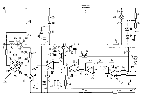
In the drawing, a first connection terminal 1 is
connected through a stabilization ballast 2 to a lamp connection
terminal 3. ~nother lamp connection terminal 4 i5 connected vla a
resistor 5 to a main electrode 6a of a controlled current limiter 6
constructed as a triac. Another main electrode 6b of the triac 6 is
connected via a coil 74 to a second connection terminal 7. The lamp
connection terminal 3 is connected through a series-combination of a
resistor 8, a resistor 9a and a resistor 9b to the lamp connection
terminal 4.
A junction between resistors 9a and 9b is connected
through a capacitor 10 and a resistor 11 to a positive input 12 of a
first operational a~plifier 13. A negative input 14 of the first
operational a~plifier 13 is connected via a resistor 15 and a capacitor
16 to the main electrode 6a o~ the triac 6. The capacitor 16 is shunted
: , : :,., -; , ~: . ~ , . . :: ,
-- 1 32 1 235
by a series-combination of a Zener diode 17 and a diode 17a with
opposite polarities.
An output 18 of the first operational amplifier 13 is
connected via a diode 19 to the negative input 14. A resistor 20 is
connected at one end to the input 14 and is connected at another end on
the one hand v'a a diode 21 to the output 18 of the first operational
amplifier 13 and on the other hand ~ a resistor 24 to a negative
input 22 of a second operational amplifier 23. A positive input 25 of
the second operational amplifier 23 is conn~cted on the positive input
12 of the first operational a~plifier 13. An output 26 of the second
operational amplifier 23 is connected through a resistor 27 ~o the
~egative input 22.
At the same time, the output 26 is connected ~ a
resistor 28 to a negative input 29 of a third operational amplifier 30.
A positive input 31 of the third operational amplifier 30 is connected
to an adjustable tapping 32 on a potentiometer 33. The potentiometer 33
is connected on the one had to a resistor 15 and on the other hand to
the main electrode 6a of the triac 6.
An output 34 of the third operational amplifier 30 is
2~ connected on the one hand vla a capacitor 35 to the negative input 29
and on the other hand ~ a resistor 83 to a positive input 36 of a
fourth operational amplifier 37. The positive input 36 of the fourth
operational amplifier 37 is also connected via a Zener diode 82 to the
main electrode 6a of the triac 6. ~n output 38 of the fourth operational
amplifier is connected y~ a resistor 39 to a base 70 of a transistor
71. The base 70 is also connected through a resistor 72 to a common lead
73, from which (in a manner not shown) the operational amplifiers
(13,23,30,37) are supplied. The transistor 71 is connected on the one
hand to the lead 73 and on the other hand ~ia a resistor 39a to a
control electrode 40 of the triac 6.
A negative input 41 of the fourth operational amplifier 37 is connected
on the one hand v a a capacitor 42 in series with a stabistor ~1 to the
main electrode 6a and on the other hand via a resistor 43 in series with
a resistor 45 to the lead 73. The positive input 12 of the first
operational amplifier 13 is connected v a a resistor 44 and a resistor
~5 to the lead 73. The capacitor 16, the potentiometer 33 and the
resistor 15 are al50 connected vla the resistor 45 to the lead 73. In
:
! ` ,
`,
' ~ ~ `.~,; ' '
' ~
1 32 1 235
turn, the lead 73 is connected through a paxallel combination
constituted by a ~ener diode 46 and a capacitor 47 to the main electrode
6a of the triac 6. The junction 44a is also connected on the one hand
via a resistor 84 to the positive input 36 of the amplifier 37 and on
the other hand ~1~ a resitor ~9 to a photosensitive transitor 50, which
is connect~dto the main electrode 6a of the triac 6. The photosensitive
transistor 50 constitutes together with a light-emitting diode 58 an
optocoupler 50-58. The photosensitive transistor 50 is shunted by a
capacitor 51. At the same time, the photosensitive transistor 50 is
connected to the base 52 of a transistor 53, which shunts the capacitor
42.
The triac 6 and the coil 74 are shunted by a parallel-
combination, a first branch of which is for~ed by a capacitor 55 and a
second branch by a series-combination of a resistor 56, a rectifier
bridge 57, a Zener diode 48 and a diode 75. The polarities of the Zener
diode 48 and the diode 75 are opposite to each other. The rectifier
bridge 57 comprises the diodes 57a,57b,57c and 57d.
Rectifier terminals 57e and 57~ of the rectifier bridge 57 are connected
to each other through the light-emitting diode 58. At the same time, the
rectifier bridge 57 is connected y~3 the diode 76 to the lead 73. The
connection ter~inal 1 is connected Y a a resistor 59, a capacitor 60 and
a diode 61 to the main electrode 6a. At the same time, the connection
terminal 1 is connected ~ the resistor 59, the capaci~or 60 and the
diode 62 to the lead 73. The diode 61 is shunted ~y a capacitor 77 and a
~5 capacitor 78 is connected to the connection ter~inals 1 and 7.
The resistors 9a and 9b are shunted by a series-co~biantion of a Zener
diode 65 and a Zener diode 66 having opposite polarities. A lamp 80 is
connected between the lamp connection terminals 3 and 4. For starting
the lamp 80, the latter ~ay be provided with an internal starter.
Alternatively, an external starter may be provided, which is preferably
connected between the lamp connection terminals 3 and 4. The circuit
arrangement shown is suitable for operating a high-pressuxe discharge
lamp at an alternating voltage supply source. The operation o~ the
circuit arran~ement can be explained as follows. The instantaneous
alternating voltage across the resistor 9b constitutes the lamp-voltage-
dependent part of the control signal S and the instantaneous
alternating voltage across the resistor 5 cons~itutes the lamp current-
.. . ,: . . ,. . , . . ,,, . .,~ ,
:, , , , : : , .,
~, . . .. .
- 1321235
dependent part. Thus, in this embodiment of the circuit arrangement,
the instantaneous values of the lamp current and the lamp vol~age,
respectively, are used for the current through the lamp IIa and the
voltage across the lamp VIa, respectively. The summation of these
alternating voltages, thus constituting the control signal S is applied
~1~ the capacitors 16 and 10 to the input terminals 14 and 12 of the
operational amplifier 13. The size ratio of the resistors 5 and the
voltage divider circuit 8,9a,9b then determines the values of B on the
one hand and C and C on the other hand.
IIa,n VIa,n
The circuit of operational amplifiers 13 and 23 forms from the
alternating voltage control signal S at the inputs 12 and 14 a rectified
signal at the input 29 of the operational amplifier 30. In the
operational amplifier 30, this rectified signal is integrated on the one
hand and is compared on the other hand with the direct voltage at the
input 31 originating from the adjustable tapping 32 on the potentiometer
33. This integration means the averaging of ISI and thus the averaging
of the absolute values of the current through the lamp and the voltage
across the lamp. The integration is effected with a time constant which
is determined by the resistor 28 and the capacitor 35. The time constant
is chosen to be large as compared with the time duration per half cycle
of the alternating voltage in which the triac 6 is non-conducting. A
time contstant of the order of the half cycle of the alternating voltage
i5 then to be preferred. Due to the integration, the possibility of
flickering of the lamp is reduced. The direct voltage originating from
the adjustable tapping 32 on the potentiometer 33 serves as a reference
signal and is fixed during adjustment of the circuit arrangement by
adjusting the potentiometer 33. This adjustment further ensures that the
influence on the switching signal due to differences ~etween individual
specimina of the circuit arrangement is strongly reduced. The said
differences are mainly due to a spread in the values of the components
used in the circuit arrangement. An auxiliary signal which is thus
obtained at the output 34 and is proportional to the control signal S is
compared in the operational a~plifier 37 as a second comparison with a
sawtooth-shaped signal in such a manner that a low voltage is applied to
the output 38 of the operational amplifier 37 as long as the auxiliary
signal is larger than the sawtooth-shaped signal, while in any other
,, - , ~ .
.. ,. . : .
,. , . . :
- .- . .; : ,., : : :
:
- , ,. : :
--` 1321235
~o
case a high voltage is applied. Thus, the operational amplifier 37
constitutes the operational amplifier intended for carrying out the
second comparison with 41 as first input and 36 as second input, which
serves as a connection for the auxiliary signal. The input 41 is
connected to a junction of the capacitor 42 and the resistor 43, which
form part of a first series-combination of a part of the circuit
arrangement for forming a sawtooth-shaped signal. The stabistor 81 is
then a first semiconductor element with diode charcteristic of the first
series-combination, and the resistor 43 the ~irst resistor. For the
capacitor 42, which is shuntable by a switch, the transistor 53 serves
as the shunting switch. The optocoupler 58-50 and the first series-
combination of the transistor 53 and the capacitor 51 together
constitute the part of the circuit arrangement for forming the sawtooth-
shaped signal.
A second series-combination connected parallel to the
~irst series-combination comprises the Zener diode 82 as the first
semiconductor element ~ith Zener characteristic and the resistor 84 as
the second resistor. A junction between the Zener diode 82 and the
resistor 84 is connected, as described, to the positive input 36 of the
operational amplifier 37. At a high voltage at the output 38, the
transistor 71 becomes conducting and the triac 6 is rendered
conducting v a the control electrode 40 of the triac. The triac 6 will
be rendered non-conduc~ing as soon as at the end of each half cycle of
the alternating voltage the current thxough the triac has fallen to a
value near zero. The voltage at the output 38 thus constitutes the
switching signal produced in the circuit arrangement.
In the non-conducting state of the ~riac 6, the circuit
co~prising the resistor 56, the rectifier bridge 57, the Zener diode 48
and the diode 75 forms a shunt in a half cycle of the supply
alternating voltage, as a result of which a so-called keep-alive current
is maintained through the lamp 80. In a next half cycle of the supply
alternating voltage, the keep-alive current flows through the circuit
46,47,76,57 dnd 56. The keep-alive current ensures that ionization in
the lamp is maintained during the non-conducting state of the triac 6,
which favours the re-ignition of the lamp when the triac 6 ~ecomes
conducting.
:: ,, , -
. .. . .
. :. :
. , ~ ., .
1 32 1 235
The keep-alive current further results in that the light emitting diode
58 emits light, so that the photosensitive transistor 50 is conducting
and hence the transistor 53 is non-conducting. The capacitor 42 will
then be charged vla the stabistor 81, as a result of which the value of
the voltage at the input 41 of the operational amplifier 37 increases.
When the voltage at the input 41 becomes egual to the voltage at the
input 36 of the amplifier 37, the triac 6 becomes conducting v a the
circuit 38,39,71,39a and ~0. However, as soon as the triac 6 is
conducting, no current will flow any longer through the light-emitting
diode 58, which results in a conducting state of the transistor 53, so
that the capacitor 42 is discharged abruptly and the Yalue of the
voltage at the input 41 decreases abruptly. As a result, the sawtooth-
shaped signal is obtained at the input 41.
~y means of the circuit 59,60,62,46 and 47, a direct
voltage is formed between the main electrode 6a and the conductor 73
and this voltage ensures in a manner not shown the supply of the
operational amplifiers 13,23,30 and 37. y~ the resistor 45, of this
direct voltage the adjustment point of the transistors 50 and 53 and
together with the Zener diode 17 and the diode 17a the adjustment point
of the operational amplifiers i5 deter~ined. The circuit elements
55,74,78 and 77 ensure that radio-interference is suppressed.
Furthermore, the coil 74 serves together with the capacitors 78 and 55
to ensure that the circuit arrangement is insensitive to any
interference pulses originating from the alternating-voltage supply
source.
The Zener diode 65 and 66 ensure that the lamp-voltage-dependent part of
the control signal S is mainly influenced by the plateau voltage of the
lamp.
The co~bination of the Zener diode 48 and the diode 75
with opposite polarities ensures together with the diode 76 and the
Zener diode 46 that the keep alive current has the sa~e value in each
half cycle of the supply alternating voltage and moreover that the
sawtooth-shaped signal at the input 41 is not dependent upon the
polarity of the alternating voltage.
The stabistor 81 ensures that a direct voltage signal is
added to the sawtooth-shaped siqnal at the input 41. The resistors 83,84
ensure that the voltage at least re~uired for a satifactory opera~ion is
, , : ,- - .:, . .
-
. . . ~ .
. ,
: ' ,.
-~ 1321235
present at the input 36 of the operational amplifier 37. It is achieved
with the Zener diode 82 that the voltage at the input 36 has a smaller
value than the maximum attainable value of the sawtooth-shaped signal at
the input 41.
In order to prevent any overload of the resistor 5, the
latter may be shunted by two diodes with opposite polarities.
A circuit arrangement of the kind described and suitable
for operating a 50 W high-pressure sodium lamp of 200 V, SO Hz , was
proportioned as follows.
resitor 8220 kOhm
9a 15 k
" 9b 2.7 k
~ 5 0.56 Ohm
" 1559 k
1110 k
" 2059 k
n 2459 k
N 27118 k
~ 28100 k
N 3910 k
39a910 Ohm
" 4316 k
~ 4459 k
N 45 5.6 k
49 16 k
N 56 4.7 k
~ 59820 Ohm
N 7210 k
N 8356 k
N 8410 k
potentiometer 33 4.7 kOhm
. . .
32 1 235
capacitor 10 0.1~F
u 16 15~F
35 0.1~F
~ 42 0.1~F
~ 47 15~F
u 51 0.1~F
55 0.068~F
" 60 0.1~F
n 77 2.2 nF
~ 78 0.033~F
zenerdiode 17 type BZX 79 B5V6 trademark Philips
46 ~ BZX 79 C15 n
i 48 ~ BZX 79 C15
~ 65 ~ BZX 79 B6V2
66 ~ BZX 79 B6V2 a
~ 82 ~ BZX 79 B5V6 Y
diode 17a type BAV 20 trademark Philips
~ 19 ~ BAV 20 n
u 21 ~ BAV 20
62 ~ ~AV 18 ~ L
61 13P~V 18 n
~ 75 ~ BAV 20 ~ ~
n 76 ~ BAV 20 ~ "
75a ~ BAV 20 n
u 57b ~ BAV 20 "
a 57c ~ aAV 20 a n
~ 57d ~ BAV 20 u
stabistor 81 type BZV 1V5 txademark Philips;
light-~mitting diode 58 together opto-coupler
photosensitive transistor 50 CNX 35, trademaxk Philips;
- , . . .
:, :. . - , :
. . . . . .
.' , ,: ~ : :
.
32 1 235
operational amplifier ~3
operational amplifier 23 together IC LM 224,
trademark Signetics;
operational amplifier 30
operational ampl.ifier 37
transistor 53 ~C 558 -:
transistor 71 BC 337
coil 2 type HP 80W/220 V-50 Hz, trademark Philips;
coil74 1.25 mH-1.6 A, Company Eichoff ~V10520
triac 6 type ~T 136-600 E, trademark Philips.
A 50 ~ high-pressure sodium lamp is operated on the
circuit arrangement thus proportioned. The lamD had a discharqe, vessel
which had a construction as known from Cana~n Patent No. 1,163,3~6
~sued Marcn 6, 1984.The electrode gap was 16.6 mm, which during
operation corre3ponded to a nominal lamp voltage VIa n of 90 V and a
nominal lamp current IIa n of 760 mA.
The filling of the discharge vessel consisted of 10 mg of mercury-sodium
amalgam containing 23% by weight of Na and xenon at a pressure of 53.3
kPa at 300 K. The colour temperature Tc of the radiation emitted by
the lamp was 2500 X.
The luminous efficacy with 100 operating hours is 50 lm/W. The value of
B is 0.4.
During operation of a 30 W high-pressure sodium discharge lamp, the
resistor 5 in the circuit arrangement is increased in value to 1 Q. At a
nominal lamp voltage Vla n of 90 V and a nominal lamp current Ila n
of 470 ~A, this corresponds to a value of ~ of about 0.3. For this 30
W lamp, it is determined by experiments what is the s~allest value of
at which the relation is satisfied Q~_ > 0. This is found to amount to
C~I -
0.26 in the case where mainly the plateau voltage influences the lamp-
voltage-dependent part of the control signal S. When also the re-
ignition peak as a whole influences the control signal S, the required Bi3 found to a~ount to about 0.4.
For a comparable lamp having a power of about 30 W, it is
1~
-- 1 32 1 235
determined by expexi~ents what is the minimum value of B with different
numbers of operating hours to satifsy the relation ~S > 0. the found
C~I
values are as follows:
100 operating hours B = 0.20
1000 operatinq hours ~ = 0.12
2000 operating hours ~ = 0.17
3000 operating hours ~ = 0.20.
For the aforementioned 30 ~ lamp, with ~ = 0.3 the influence of an
abrupt variation of the supply alternating voltage has been determinded
at the average lamp voltagel the colour temperature Tc and the
coordinates of the colour point. The abrupt variations are 10% with
respect to the nominal supply voltage of 220 V. The results are
indicated in Table I during operation with the circuit arrangement and
in Table II during operation without the circuit arrangement.
TABLE I
Supply alternating voltage ~V) 198 220 242
average lamp voltage (V) 102.3 104.8 105.6
colour temperature TC(K) 2470 2493 2498
20 coordinates of the colour point x.483 .481 .480
y.419 .419 .418.
TABLE II
Supply voltage (V) 198 220 242
25 average lamp voltage (V) 72.1 88.9 113.7
lamp power (W) 24.9 31 43.9
colour temperature TC(K) 2205 2453 2980
coordinates of the colour point x.515 .481 .436
y.430 .419 .402
The values of the average lamp voltage indicated in Table I are
comparatively high due to the strongly increased re-ignition peak with
the use of the circuit arrangement as compared with the operation of the
lamp without thP circuit arrangement. The indicated lamp voltage values
are measured according to the R.M.S. principle. However, it is
remarkable that a variation of 10% in the supply voltage with the use of
the circuit arrangement re~ults in a variation of the average lamp
voltage of not more than about 2%. Without the use of the circuit
.
:::: , , . , .. : . :
..
:
.
~ 1 32 1 235
arrangement, on the contrary, a variation in the average lamp voltage up
to even 28~ is obtained.
Two 30 W lamps of the same type as described above are operated in the
same manner without the use of the circuit arrangement described. The
5 most important results are: .
lamp 1 lamp 2
Average lamp voltage (V) 79.R as ~ 9
Colour temperature TC(K) 2309 2453
Coordinate of the colour point x.502 .485
y.426 .420
With a corresponding operation with the use of the circuit arrangement
described, the results are:
lamp 1 lamp 2
Average lamp voltage (V) 101.3 104.8
15 colour temperature TC(K) 2470 2493
coordinates of the colour point x.483 .481
y.419 .419.
: , : , : . ~ , : . :
: ~ - ~ . , . . : .