Note: Descriptions are shown in the official language in which they were submitted.
l321298
ALIGNMENT OF LITHOGRAPHIC SYSTEM
This invention relates to the Eabrication of devices, and in particular, the
fabrication of devices requiring the registration of lithographic patterns.
The background oE the invention will be described in detail hereinbelow.
Tlle inventive procedure for an exposure system, such as a deep ultraviolet
5 exposure system, allows calibration and alignment using the exposing wavelength with
alignment occurring in the exposure position. This alignment is preferably performed by
using an initial calibration with the exposing light through the exposure lens system and a
subsequent direct optical alignment. Thus, through this specific division of steps all the
desired expedients are employed to provide excellent alignment accuracy.
The calibration is performed by projecting through a ~Iducial mark on the
reticle or mask onto a substrate coated with a calibration material such as a photochromic
material where the substrate is positioned on the substrate holder, i.e., the translation
stage. (A photochromic material is one which undergoes a change of at least 5 percent in
absorption or a change of 0.01 in refractive index when exposed to the calibration light at
15 a light intensity that does not induce unacceptable mechanical degradation of the
photochromic material.) The fiducial mark in the mask or reticle is designed to produce a
pattern in the calibration material that is capable of inducing sufficient diffraction. Two
beams of light having essentially the same phase and having essentially the samepolarizations are intersected at a glancing angle over the projected ~1ducial mark. (The
20 glancing angle generally avoids interference with the lens system.) The relative phase
and/or path length of the intersecting beams are adjusted to produce an inter~erence
pattern above the diffraction grating and an interaction of this interference pattern with
the diffraction grating that produces a diffracted light intensity quantifiable by the
detection electronics, e.g., an observable extremum, in the resulting beams of diffracted
25 light. The position of the calibration diffraction grating yielding this reference diffracted
Iight intensity corresponds to the position desired for an equivalent diffraction grating
fiducial mask on the substrate to be processed.
After calibration, alignment is achieved by placing the substrate to be
processed with its overlying photosensitive material and its diffraction grating fiducial
30 marks onto the translation stage of the exposure tool. The substrate position is
determined using, for example, conventional expedients such as the global alignment tool
of the exposure apparatus. The stage is then proximately positioned for exposure. The
A
, ~.... ..
~ . ~.. -
.. ~ ~ . . .
2 132~ 2~8
fiducial mark on the substrate (corresponding to the fiducial mark on the reticle or mask)
is then aligned by observing, as a function of stage position, the intensity behaviour of the
diffracted light intensity induced by the interaction between the previously adjusted
intersecting beams and the fiducial di~fraction pattern--the desired alignment position
corresponding to the position yielding the reference diffracted light intensity. In this
manner, alignrnent relies on the initial cslibration utilizing the exposing wavelength
through the exposing lens system and the subsequent optical observation during the rlnal
alignment in the exposure position. The desired criteria for accurate registration are
achieved and excellent reliability is attained. Additionally, even without the calibration
technique, improvement over many alignment systems is still obtained using the
intersecting beam approach.
In accordance with one aspect of the invention there is provided a method
for fabricating a device formed from a device substrate, said substrate including an
alignment mark and a radiation sensitive material comprising the steps of 1) positioning
said substrate for lithographic exposure by employing said alignment mark, 2) exposing
said substrate to said radiation through a mask or reticle to delineate a pattern in said
radiation sensitive material, and 3) progressing towards the completion of said device by
employing said delineated pattern characterized in that said alignment mark is capable of
diffracting light and said alignment is accomplished by A) intersecting at least two beams
of said light at said mark wherein said intersecting beams and said alignment mark are
such that an interference pattern is formed that is diffracted from said mark and B)
positioning said substrate based on an optical characteristic of said diffracted light.
The present invention will be described hereinbelow with the aid of the
accompanying drawings, in which:
FIGs 1 and 2 illustrate apparatuses involved in the invention; and
FIG 3 is illustrative of optical configurations involved in $he invention.
In the manufacture of devices such as integrated circuits, a pattern is
produced through lithographic processes in a radiation-sensitive material coated on a
device substrate. (Substrate, for purposes of this disclosure, is a body, e.g., a
semiconductor body, that is being processed into a device or plurality of devices, e.g.,
semiconductor devices. This body could include not only semiconductor materials or
optoelectronic materials, but also regions of organic materials, metals, and/or dielectrics.)
These processes generally involve a series of exposures over the radiation-sensitive
. ~
,:~
3 1321298
material, e.g., a resist, in a desired repeated pattern by light projected through a mask or
reticle and focused onto the photosensitive material with a suitable lens system. However,
the substrate before each exposure must be positioned relative to the projected pattern
(generally by use of a translation stage, controlled by a position measuring device such as
5 an interferometer~ so an appropriate spatial alignment is obtained between the projected
image and device patterns on the waEer.
One method of alignment is a global technique. In this procedure to
calibrate the system a sample waEer having appropriately positioned alignment mark(s)
underlying a radiation-sensitive layer is, for calibration, moved into the viewing field of a
10 microscope, 31 FIG. 1, external to the exposure lens system. The substrate alignment
marks are aligned with the reference fiducial mark(s) of the microscope. The substrate is
then moved to the exposure position under interferometric control. The distance of
movement is calculated from the known position of the microscope fiducial mark and from
the desired position of exposure.
The substrate is then exposed utilizing the reticle to be employed in the
device fabrication. The reticle pattern includes an alignment mark (generally a vernier
series of marks) that is projected onto the radiation-sensitive material. The radiation-
sensitive material is developed and the spatial separation of the projected alignment mark
relative to the wafer alignment mark, i.e., the spatial error, is determined by optical
inspection. After calibration, for device production, the device substrate being processed
is initially aligned using the microscope fiducial marks. The substrate is then positioned
for exposure by, for example, interferometry employing a suitable correction for all
positioning as previously determined by the global calibration. Subse~uent, positioning is
done by dead reckoning from one exposure position to the next on the substrate.
The relative large dead reckoning translations associated with the global
alignment technique introduces a concomitant error. In a second approach denominated
a site-by-site technique, a separate alignment measurement is performed for eachexposure on a wafer during production, and thus, less error is typically introduced. In this
technique there is an alignment mark(s) on the wafer for each fabrication exposure to be
performed. Be~ore each fabrication exposure there is an alignment at the correspondmg
alignment mark and then movement rom the alignment position a known, relatively short,
distance to the fabrication exposure position.
:
,f,~i
, ~ ~....
.. . ... .
..
; , :. ,
,, ~. . ~ , : ,
4 132~298
A more desirable approach for a site-by-site alignment procedure would use
the exposing wavelength to project a fiducial mark on the mask or reticle through the
imaging lens with alignment accomplished between this projection and a corresponding
mark on the substrate without the necessity of moving the substrate between alignment
S and fabrication exposure. In this manner, it would be possible to eliminate errors
associated with 1) wafer movement and with 2) assumptions based on both the indirect
measurement oE distance and on the equivalence oE di~ferent lens systems to diEferent
wavelengths. In practice it is difficult to employ this desired approach. It is usually
undesirable to employ the exposing wavelength for alignment because the radiation-
10 sensitive material on the substrate generally is irreversibly modified in the region of thealignment marks (fiducial marks). This premature exposure is undesirable because the
alignment mark necessary for subsequent alignment in the ne~t device layer is often
obliterated. Additionally, deep ultraviolet light is often strongly absorbed by the
photosensitive material, and thus, does not illuminate the mark on the wafer.
Since it is generally not desirable to use light of the exposing wavelength for
alignment, the use of the exposure lens system is also often precluded and alignment is
done at a place removed from the exposure position even in systems that align through
the exposure lens. (This limitation is especially severe for deep ultraviolet exposure
systems--systems operating with light in the wavelength range 350 to 180 nm.) The
20 exposure lens system is designed for the wavelength of the exposing light, and thus, causes
optical distortions when used with a different wavelength. The greater the difference in
wavelength between the aligning and exposing ligh~, the greater the distortion. Generally,
longer wavelength light (light in the wavelength range 5000 to 11,()00 Angstroms) is used
for alignment to avoid exposure of the resist material. Such light, e.g, red light from the
25 ~IeNe laser, is so far removed from the deep ultraviolet region of the spectrum that gross
distortions would occur if the exposing lens system is utilized for alignment. Additionally,
the anti-reflection coatings on the exposure lenses often produce large reflections at
wavelengths other than the exposure wavelength. Some site-by-site systems compensate
for these effects by placing special but small optical elements in the exposure lens. These
30 elements are usually located at the edge of the exposure field where they do not interfere
with normal operation. However, for stability, these elements are fixed in position, and to
be aligned the alignment mark on a wafer must be moved under these elements and away
from the exposure position.
~s
, ......
s 13~1298
For these reasons, site-by-site alignment is generally done with the device
substrate positioned on the edge of the lens system, either outsis3e the lens barrel as
shown in phantom at 60 in FIG. 1 or at the very edge of the exposure field, to allow non-
distorted introduction of the aligning light. Reflection is observed with a monitor, e.g., a
television camera or the microscope. The optical axis or other known fiducial mark
position of the microscope is calibrated relative to a point of reference. The reticle
fiducial mark is calibrated relative to the same point of reference. The stage is then
moved to alignment using interferometric techniques a calculated distance based on the
two calibration measurements and optical alignment measurement. Clearly, numerous
errors are possible ;n calibration, measurement, and movement. Thus, although alignment -
techniques have been satisfactory for presently used wavelengths (the blue and near
ultraviolet wavelengths) and/or for design rules of 0.9 ,um and larger, improvement is
certainly possible. Additionally, for deep ultraviolet lithographic systems serious difficulties
and unresolved impediments are presented.
Although for pedagogic reasons the invention is described in terms of a
deep ultraviolet exposure system, the invention is not lirnited to this spectral range. `!'
Indeed the invention is suitable for any exposure system including those utilizing X-ray,
ion, and electron exposing radiation.
A. Initial Calibration
Calibration is performed by using a diffracting pattern, e.g., grating pattern,
fiducial mark on the reticle or mask. (Generally, but not necessarily, a fiducial mark for
direction positioning and a separate one for y direction positioning together with separate
alignment systems for each is employed. However, the lines of the grating need not be
parallel to these directions.) This fiducial mark should be in a pattern that produces a
diffraction grating having a period that is equal to, or an integral multiple of, the period of
the fringes produced by the intersecting beams. Small deviations from integral multiples is
acceptable and do not produce substantial error. Generally, the larger the number of
fringes in the grating, the smaller the deviation allowed to maintain the same error level.
If the number of fringes is the same, larger gratings require smaller deviation. However,
the number of fringes has a substantially larger effect on error than grating size.
,"~, ~
,..~
: , .: : :............. . .
- . ~
, ~. ; , ~ . '
5 a 132~L2~8
Typically, it is desirable to have a fractional deviation less than 1/2N where N is the
number of fringes. (If a reticle is utilized where the reticle is proportionally bigger than
the image ultimately projected, the period of the mark on the reticle should be such that
the projected image has the desired diffraction grating spacing.)
S The exposed material utilized for making the calibration is not critical
provided a diEfraction pattern corresponding to the projected image and having aresol~ltion of at least half oE the grating period is produced upon exposure without the
necessity of moving the wafer from the translation stage for development. It has been
found that photochromic materials such as 1,3,3 trimethylindoino-6'-Nitrobenzopyrylo
spiran intermixed in polymers such as poly(methyl methacrylate) at concentrations in the
range ~0 to 80 percent are suitsble. The exposing
At~
.. . .
-
- 6- ~321298
radiadon should produce a difference in refracdve index between lines and spacesin the calibration material of at least 0,01 and/or a change in absorpdon of at least
5 percent. The calibration material, e.g., the photochromic material, is subjected
to the exposing wavelength through the reticle tor mask) and through the lens
S imaging system ultimately to be utilized in the lithographic process. (This
calibradon technique of using a material that undergoes a discernible optical
change without movement of the calibradon material off the transladon stage
before calibration with this optical change is advantageously employed in
alignment schemes even withou~ the subsequently described intersecting beam
10 calibration and alignment techniques. For example a calibration vernier is
projccted onto the calibration material. The vernier is then moved under a global
alignment microscope redicule and the calibration correcdon determined from the
known distance moved and the known posidon of the global alignment redicule.)
Two beams are directed to intersect above the calibration diffraction
15 pattern produced in the calibradon material. (If the calibration material undergoes
a perrnanent or temporary refracdve index or absorpdon change, the exposing
radiation need not be maintained once the grating is formed.) It is possible to
control the posidon of intersecdon, ~i.e., move the aligning light to the mark, not
the mark to the aligning light as in most site-by-site aligners) by conventional20 techniques such as moving the incoming bearn along the direction y (or vertical)
in PIG. 1 and/or by moving the prism, 13, along the direction x (or horizontal).The intersecdng beams are brought in at the shallow angle denoted 40 in FIG. 3.
13y utilizing a glancing angle, it is possible to rnake the light incident on the
calib~a~on material and avoid interference with lens 70 of the imaging system.
25 The angle relative to the substrate thus, should generally be sufficiently low so
that the beams do not substandally impact the lens system. However, angles less
than approximately S degrees induce substantially increased reflecdon at the
calibration surface, and thus, although not precluded, are less advantageous.
Gerlerally, an inciden~ angle of between 5 and 25 degrees is employed. (In some
30 lens systems it is not possible to introduce the light below the lens system.However, advantage is still possible by calibrating and aligning outside the lens
system using intersecdng beams in the pr¢viously-described site-by-site approach.
It is even possible to do this type alignment in the exposure posidon. For
example, the alignment marks on the substrate are sufficiently spatially removed35 from the corresponding pordon to be exposed that they are beyond the exposurelens system when this portion is in the exposure position.) Additionally, if an
.
-7 ~21298
exposure lens is not employed, such as in electron beam exposure, or if alignment
is done outside the lens, angles up to and including 90 degrees are acceptable.
It is generally desirable for the intersecting light to be in the
wavelength range 500 to 1100 nm. For example, a 6328 Angstrom line from a
5 HeNe laser is employed. Light in this wavelength range is employed generally
since below 5000 Angstroms the resist material utilized in the subsequent
alignment step typically is exposed by the radiadon. Generally, the intersecdng
beams should have power at the alignment surface of at least 1 microwatt.
Powers less than 1 micr~watt lead to excessive noise. For stability, the path
10 lengths of the two intersecting beams should be generally reladvely close, e.g.,
should be within 5 cm for HeNe light. However, for thermal stability of the
system it is advantageous to have the path lengths as close as possible. This isaccomplished, for example, by ob~aining the two bearns from a single laser bearnthat has been split by conventional opdcs such as polarizing bearn splitters,
15 dielectric or metallized beam splitters. Addidonally, the reladve angle between
the two beams, 50 in FIG. 3 should be in the range 5 to 30 preferably 10 to 15.
Larger angles lead to the loss of higher order diffraction from the underlying
calibradon pattern, and thus, limit the region in which detection is possible.
Smaller angles form large fringe periods and result in a degradation of accuracy.
20 Thus, although not precluded for this reason, lower angles are less desirable.
Exemplary of suitable conditions is the angle of 13.36 degrees between the beamsand 20 degrees between a beam and the substrato for a 3 llm period and HeNe
laser light.
The intersecting beams above the calibration su~face produce an
25 intelference pattern including light and da~l~ lines denorninated fnnges. Ihe size
and penod of this patte~n is adjusted by changing the angle between the two
beams. The size of the pat~ern and the period should be chosen to yield more
than 10 lines in the grating to maintain accuracy. The size of the pattern on the
wafer is typically in the range 50 to 200 llm. Pattems larger than 200 ~lm occupy
30 excessive wafer space. The period is typically in the range 2 to 8 ~m. Th
inter~erence pattern intelacts with the diffrac~ion gra~ng produced in ~he
calibration material. It is generally desirable to adjust the beams so that the
resulting interference patterll fills the entire diffraction ~a~ng, although partial
filling of the grating is not precluded. The inte~ction of the interference pattern
35 w,ith the grating produces a series of di~fraction orders as shown in FIG. 2.Gene~ally, dle (1,1), i.e., the first or~er of diffracdon, is monitored because it iS
'` : ` :
.
- 8 1321298
syrnrnetric and only one, not two, photodiodes need be used with the concomitantsimplification in signal processing. However, it is possible to obtain accurate
results by monitoring any pair of the obseNable diffraction orders. The relativephase of the intersecting beams is adjusted through expedients such as changing
S the angle of a glass plate, and/or moving a mirror, or electrooptic crystals, until a
reference intensity, e.g., extremum, is observed in the diffraction order being
monitored. This reference intensity denotes the appropriate positioning of any
fiducial mark on the substrate relative to the corresponding fiducial mark of the
reticle or mask. .
B. Alignment
The calibratmg substrate is removed and the substrate to be processed
is placed on the translation stage substrate holder. The substrate is moved intoapproximate alignment. This proximate alignment is accomplished by determining
the posidon of the wafer holder by the conventional global alignment utilizing
1~ interferometric techniques, and moving the substratc holder stage by, for exarnple,
interferometry to the approximate alignment posidon. The diffraction gratings inthe substrate corresponding to the fiducial mark of the reticle or mask is subjected
to the same intersecting beams as adjusted in the calibrating procedure. (If
diffraction gradng calibration is not performed, the pa~meters previously
20 described for use in the calibradon are used in the alignment.) These intersecting
bearns upon interaction with the diffraction gratings fiducial mark in the substrate
produces diffraction orders similar to those obtained during the calibration
procedure. Ihe position of the substrate is then adjusted to again obtain the
reference diffraction intensity, and thus, to accurately align the fiducial mark of -
25 the substrate w~th ~he fiducial mark of the mask or reticle. If a plurality of
exposures are to be made, it is possible to repeat the alignrnent procedure for each
alignment mark.
In a preferred technique the monitoring system includes a
photodetector such as a silicon photo~ode and processing electronics that detect
30 an enor signal such as boxcar inte~ators, phase sensitive detection, and tuned
amplifiers. (The difference between the photodetector signal and the reference
signal is detected and the resulting e2ror signal is fed back to fhe exposure tool
which moves the substrate to minimize the error signal.) It has also been found
convenient to move the optical f~inges in a reciproca~ng pattern around the
35 approximate alignment position. The resulting diffraction order yields an intensity
variation. By using this reciprocal movement and electronics such as boxcar
:~, . ,,. ,: :
" , .,
,
~i " .~
-9- 132~2~
integration, phase sensitive detecdon, and tuned amplifiers, errors a~e reduced by
averaging. Nevertheless, such reciprocal movement is not required.
The following exarnples are illustrative of condidons useful in the
invendve process.
5 Example 1
The alignment system was physically attached to the global alignment
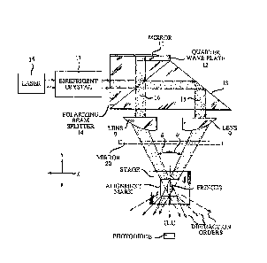
structure of a GCA DSW- Wafer Stepper 4800 stepper. The optics for introducing
the intersecting 'oeams at the substrate in the exposure position is shown in FIG. 2.
The HeNe laser (663 nrm), 15, had a pc.wer output of approximately 2 milliwatts.10 The laser position around an axis along its long direction was adjusted so that the
emanating light had a polarization plane that was approximately 45 degrees to the
major surface of the substrate. The beam was directed through a quartz
birefringent crystal. The birefringent crystal was X-cut and was positioned so that
s nall rotations of the crystal produced corresponding small oscillations in thc15 difference of phase between the horizontal and vertical components of the laser
light. The system also included 1) a polarizing beam splitter, 14, that reflected the
honzontal polarized componen~ of the light and ~) a quar~r wave plate, 12, with a
rni~sor, 11. The quarter wave plate and tns mirror were chosen sc. tnat the
horizontal light entering the quarter wave plate was reflected from t'ne mirror,20 again ~ransversed the quar~r wa~re plate, and exited as ver~cally polarized light.
Two lenses, g, having a focal length of approxima~ely 70 millimeters were
posidoned ~o reduce the 'oeams, 15 and 16, from a diameter of approximately
1 millimeter to a diameter of approximately 0.2 millimeters at the substrate
surface. The lenses weIe posidoned so that the angle a between the two beams
2S was approximately 6.0~ deg~ees. Addidonally, a mi~or shown in phantom, 20, in;. 1 and in FI~. 2 was inserted so that the beams weqe reflected towards the
substrate and made an angle of approximately 20 de~ees relative tO the substrate.
S~ven silicon photodiodes with a photosensitive area of approximately
3 ~ete~s diameter was positioned to detect the va~ious orders of diffracted
30 light produced duIing subs~ate ca~ibration and alignment. Their positioning was
accomplished with a controlled sample.
The cont~olling elec~ro~cs included a boxcar ineegrator that compared
a square wave signal u~lized to oscillate the birefringent crystal to the ac
component of the signal from the photodiode of the order being ntili7e~d for
35 alignment. The output of this integrator was a dc error signal that was
',. ` ` ~ ,' ` : `
. .
:
- lo- 1321298
proportional to the error in the ac component. Electronics were fur~er provided
for feeding this error signal back to the posidoning electronics of the stepper. The
stepper translation stage under the influence of this feedback was moved to yield a
rninimum in the ac componen~ of ~he photodiode output. Electronics was also
5 provided so that when the alignment as measured by the amplitude of the error
signal was better than 0.1 micrometers exposure by the stepper was automaticallytriggered.
Calibradon of the Apparat~s
A reference wafer was produced by applying a few drops of a soludon
10 containing 80 percent of 1,3,3 trimethylindoino-6'-nitrobenzopyrylo spiran,
20 percent of poly(methyl methacrylate) and then dissolved at a 1:10 rado in a
solvent. The wafer was spun at the rate of about 3000 rpm to yield a final
photochromic layer thickness ~ 1 llm. The wafer with the photochromic side
exposed was placed on the sample holder of the stepper. The wafer was
15 posidoned by the automadc handling system of the stepper. A ~inch (5:1) quartz
reticle approximately .040 inch in thielsness was posidoned in the redcle holder of
the apparatus. This reticle included a series of electrically probable test patterns
similar to those described in VLSI Electronics, N. Einspruch, ed., p. 320,
Academic ~ress, 1987, a series of spatially distnbuted opdcal ve~niers, and an
20 alignment ma~k that measured 1.5 millimeter square and had a pe~iod of
approximately 30 micrometers. The reticle was positioned utilizing alignment
marks for that pulpose on its holder by observadon ~hrough an optical microscope.
The sample was moved so that the photochromic su~face was in the exposure
position. The photochromic material was then exposed through the reticle using
25 the mercury discharge expos~e lamp (405 nanomcters). The exposure was
maintained for approximately S seconds at an intensity of several hundred
milliwatts per squa~c centimeteT. After exposure, the int~secting beams of the
ali~ment optics utilizing the equipment shown in FIG. 2 was directed along
path 80 to intersect a~ ths resul~ng diffraction grating in the sample. SThe
30 inte~don point of the beams had previously been adjusted to be posi~oned at
the point of exposure for the alignment mark.) The feedback electronics from theboxcar integsator to the stepper electro~ics was disconnected. The dc bias to dle
biref~ingent crystal was adjusted to yield a ~um in the ac output of the
photodiode monitoring the central diffraction order. The photoshromic sample
35 wafer was then removed.
. .
,- . ,. i . . .
- . ~ .. ..
11- 1321298
A 4-inch wafer was then used to test the alignment system. This
wafer included a 3500 Angstrom thick overlying layer of silicon dioxide coveringthe entire surface, and an overlying layer of tantalum silicide of thickness
2500 Angstroms having 1) the pattern of the first level of the electrically
S probeable test pattern, 2) the corresponding op~ical vernier marks, and 3) thediffraction grating alignment marks. (Tantalum silicide was chosen because of its
advantageous electrical properties for electrical probeable testing.) A tri-level
resist was utilized over the tantalum silicide layer. This resist included a 1.1 ~lm
thickness layer of novolac material overlaid by a 0.12 ~lm thick layer of silicon
10 dioxide which, in turn, was overlaid by~a 0.6 ~lm thick layer of Shipley #1822
positive photoresist.
The sarnple wafcr was positioned on the transladon stage of the
stepper utilizing the automatic wafer handler. A global alignment was performed
with the global alignment optics, 31, supplied with the GCA steppcr. After global
15 align;nent the wafer was moved to ~he approximate yosition for the first exposu~e.
The feedback loop between the boxcar integrator and the stepper was connected.
The electronics was allowed to align thc wafer by minimizing the ac signal and
upon suitable alignment to perform the first exposure. The alignment system was
maintained during the entire exposure. The eleetTonics for ali~nment was then
20 disconnected and the stepper was allowed to approximately position the wafer for
the next exposure. The alignment procedure and exposure was then repeated. A
series of exposures on the same wafer was also done utilizing global alignment
but not the intersecting beam alignment technique. The sample was then removed
from the stepper, developed, and processed by conventional techni~ues.
The misalignment for the vanous exposures was measured as
described in Einspruch, supra. ~e best results ~or the site-by-site techniques
showed a standard deviation of e~or consistently around 0.3 llm and showed an
en~ as good as .003 llm. The globally aligned samples although at dmes
showing egl~ivalent eror had a ve~y large standard deviation and poor consistency.
Eor some exposed samples for a given reticle it was found that a
constant eIror was obtainedi. To co~ect for this error a~ter calibration the dc bias
of the birefnngent crystal was adjustedi. This one-time adjustrnent was found tobe necessary generally when the machine was completely reconfigured or for like
changes in exposure condidons.
35 Exam~le 2
'. ; '
' ~ ~
- 12 ~3212~
l'he prscedure of Exarnple 1 was followed except the alignment
electronics was turned off during exposure of the sample and a constant signal
was maintained on the translation stage.
. . . , ~ ~ . , .- ~ , .
, ",
- . : ~ - , : , ;
.