Note: Descriptions are shown in the official language in which they were submitted.
1321616
G-1160 C-4044
IGNITION SYSTEM DWELL CONTROL
This invention relates to a dwell control
system for an electronic internal combustion engine
ignition system and more particularly to a control
circuit for developing a compensated digital signal
that is a function of a time period beginning with
energization of the primary winding of an ignition
coil and ending when primary winding current
increases to a current limit value.
The ~nited States Patent to Neuhalfen et
al 4,711,226 diQcloses a dwell control system
wherein the ramp or rise time of the primary
winding current of an ignition coil is determined
where the ramp time i~ a time period beginning with
energization of the primary winding of an ignition
coil and ending when primary winding current
increases to a current limit value. This i~
accomplished by counting clock pulses in a ramp
counter where the counting begins when the primary
winding is energized and where counting terminates
when primary winding current increases to a sensed
current limit value. When primary winding current
increases to a sensed current limit value, a
current limit signal i8 developed and a transistor
that controls primary winding current is biased
into a current limiting mode. The transfer
function of the current sensing amplifier of the
patent is non-ideal so that it may develop a
~r
~,
-- .
.
1321616
current limit signal at less primary winding
current than a desired or specified current limit
value. By way of example, the current limit signal
may be developed when primary current increases to
90% of the desired current limit value. In order
to compensate for this inherent error mechanism,
the closed loop dwell circuitry of the Neuhalfen et
al patent uses preset values, which are added to
the ramp time, to model the 10% inaccuracy. The
preset value is determined from the ignition coil's
previous ramp time. This preset value i9 loaded
into the ramp counter before the present start of
dwell (SOD) occurs. Once dwell begins, the ramp
counter containing the preset, begins counting.
When a current limit signal occurs, counting by the
ramp counter ceases. Thus, the ramp counter
contains all of the ramp time before the current
; limit signal occurs, plus a fixed number to
compensate for the error.
The system of the Neuhalfen et al patent
has a limited number of fixed presets for the full
range of coil ramp times and accordingly these
presets do not accurately represent the continuous
10% dwell inaccuracy. The more ramp time decodes,
and hence fixed presets, the more accurate the
model. However, the greater the number of decodes,
the larger the programmable logic array (PLA) used
; in the Neuhalfen et al patent becomes in order to
process the decodes and choose the correct preset.
This consumes large amounts of silicon area.
Further, the PLA will never be completely accurate
- .
1321616
unless a separate decode and preset are available
for every possible ramp time.
In the Neuhalfen et al patent, the system
divides the ramp time into only three ranges. Even
this small set of ranges requires a large PLA and
~witching circuitry that could total as high as 700
transistors.
The present invention elimirates the PLA
used in the Neuhalfen et al-patent. Instead of
using a PLA, the present invention uses a ramp
counter of the type disclosed in the Neuhalfen et
al patent that cooperates in a unigue manner with a
down-counter. The ramp counter is an up counter
and it counts constant frequency clock pul~es for a
period of time beginning when the primary winding
of an ignition coil is energized or start of dwell
(SOD), and ending when a current sensing amplifier
develops a signal indicative of the fact that
primary current has increased to a sensed current
limit value. The count in the ramp counter
represents ramp time. When the current limit
signal is developed, the most significant bits of
the ramp counter are loaded into the down-counter.
The ramp counter is now incremented or counted-up
and the down-counter is now decremented or
counted-down at a constant frequency. This
continues until the down-counter underflows
whereupon the up-counting of the ramp counter and
the down-counting of the down-counter is
terminated. The net effect of this is that the
ultimate or final count in the ramp counter will be
equal to the count attained by the ramp counter
1321616
between SOD and Qensed current limit added to a
fixed or constant percentage of the attained count.
Since the count in the ramp counter represents
elapsed time, the final count in the ramp counter
represents ramp time added to a fixed percentage of
the ramp time. It will be appreciated that the
syQtem of this invention will respond to the entire
ramp time range.
It accordingly is an object of thiQ
invention to provide a new and improved control
circuit for developing a compensated digital ~ignal
that is related to ramp time wherein a ramp counter
is incremented for a period of time beginning when
the primary winding of an ignition coil is
energized and ending when current limit is reached
and wherein the count attained by the ramp counter
during this period of time is proceQsed to provide
a digital signal that equalQ the count attained by
the ramp counter added to a fixed percentage of the
count attained by the ramp counter.
Another object of thiQ invention is to
provide a system of the type described wherein the
processing of the count attained by the ramp count
is accomplished by the use of a down-counter and
wherein the most significant bits of the count
attained in the ramp counter iQ loaded into the
down-counter and wherein the ramp counter is then
counted-up and the down-counter counted down until
the down-counter underflows. The final or ultimate
count in the ramp counter haQ a count magnitude
that is equal to attained count added to a fixed
percentage of the attained count.
~ ` ~
1321616
In the Drawings
Figure 1 illustrates a current waveform
where the primary winding current of an ignition
coil is plotted again~t elapsed time; and
Figure 2 illustrate~ a control circuit
made in accordance with this invention.
Referring now to the drawings, Figure 1
illustrates a waveform of the primary winding
current of an ignition coil plotted again~t elapsed
time. In Figure 1, the primary winding of an
ignition coil is energized at the start of dwell
(SOD) by biasing a switching transistor conductive.
The primary current now increases and ramps up
along ramp curve or line 10. When primary winding
current reaches a predetermined desired current
limit value at point 12, the switching transistor
that controls primary winding current is biased
into a current limit mode. When thi~ happens,
primary winding current is held at a substantially
con~tant value depicted by line 14. The time
reQuired for primary winding current to attain the
current limit value i~ the ramp time and it is
depicted in Figure 1 for the case where current has
attained the desired current limit value. Also
depicted in Figure 1 is a current level which is
identified as 90% of the current limit value. This
occurs at a point identified by reference numeral
13. At the end of dwell point EOD the tranqi~tor
that controls primary winding current is biased
nonconductive to cause spark plug firing from the
secondary of the ignition coil.
: . ' :
. .
~ ~ '
1321616
The optimum spark event occurs when EOD
occurs just after current limit is reached, that
is, the transistor that controls primary winding
current should be biased nonconductive immediately
after point 12 of the waveform of Figure 1. This
allows the ignition coil to generate enough energy
to cause the spark plug to fire, without excessive
power dissipation which could be caused by
operation for too long a time period in the current
limit mode along line 14.
In describing the dwell control of this
invention which is illustrated in Figure 2,
references will be made to the system disclosed in
the above mentioned United States patent to
Neuhalfen et al. 4,711,226.
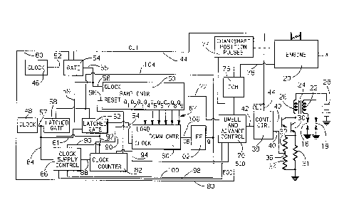
Referring now to Figure 2, the reference
numerals 16 and 18 designate spark plugs for a
spark ignited internal combustion engine 20. These
spark plugs are connected to the secondary winding
22 of an ignition coil 24. The primary winding 26
of the ignition coil is connected between a source
of direct voltage 28 and Darlington switching
transistor 30. Darlington transistor 30 is
connected in series with a current sensing resistor
31. Voltage divider resistors 32 and 34 having a
node or junction 36 are connected across resistor
31. When transistor 30 is biased conductive
primary winding current flows through primary
winding 26, through transistor 30 and then through
30 current sensing resistor 31 to ground. The voltage
that is developed at junction 36 is a function of
~' .
1321616
primary winding current magnitude and this voltage
follows the waveform shown in Figure 1. The
voltage at junction 36 is applied to a control
circuit 38 via line 40. The control circuit 38 is
5 further connected to the ba~e of tranqistor 30 by
line 42 and to a line 44. A current limit signal
CLI is developed on line 44 whenever primary
winding current attains a current limit value. The
control circuit 38 applies a square wave signal to
line 42 which causes transistor 30 to be biased
either conductive or nonconductive. The control 38
takes the form shown in Figure 3 of the
above-referenced Neuhalfen et al patent.
When an SOD signal transition is applied
to line 42 transistor 30 is biased to a conductive
saturated condition. Primary current now increases
along ramp line 10. When primary winding current
reaches a current limit value, the voltage
developed at junction 36 causes transistor 30 to be
20 brought out or sat,uration and to come biased into a
current limiting mode (line 14 of Figure 1). When
it is desired to fire spark plugs 16 and 18, a
signal transition occurs on line 42 which biases
transistor 30 nonconductive. When transistor 30
25 goes nonconductive, a voltage is developed in
secondary winding 22 to cause plugs 16 and 18 to be
fired.
The system of Figure 2 has two clock
pulse source~ designated respectively as 46 and 48.
30 The clock 46 develops square wave clock pulses at a
constant frequency of about 10 Khz where engine 20
is a four cylinder engine. If engine 20 were a six
13216I6
cylinder engine, the frequency of clock 46 would be
about 16 Khz. The clock 48 also develops ~quare
wave clock pulses at a constant frequency that is
higher than the frequency of clock 46. Thus, the
frequency of clock 48 may be about 125 Khz.
The clock 46 is connected to the clock
input of a ramp counter 50 via line 52, gate 54,
line 55 and line 56. The counter 50 is an
up-counter. As will be more fully described
hereinafter gate 54, is actuated to a clo~ed
condition wherein it' connects clock 46 to the clock
input of counter 50 at SOD or in other words at the
time transistor 30 is biaQed conductive. Gate 54
is actuated to an open condition by a signal
developed on line 44 to terminate the application
of clock pulses to counter 50 when primary winding
current increases to a current limit value to
thereby cause transistor 30 to be biased into a
current limit mode.
The clock 48 i~ connected to the clock
input of up-counter 50 via line 57, latched gate
58, line 59 and line 56. The clock 48 is also
connected to the clock input of a down counter 60
via line 57, line 61, latched gate 62 and line 64.
As will be more fully described hereinafter, the
gate~ 58 and 62 are at times actuated to a closed
condition to connect clock 48 to counters 50 and
60.
The counter 50 is a nine-bit up-counter
and the counter 60 is a six-bit down-counter. As
will be more fully described hereinafter, the six
most significant bits of counter 50 are
1321616
periodically loaded into down-counter 60 via the
six bit lines 67 that are connected to bit output
terminals Q4-Q9 of counter 50. The counters 50 and
60 are so-called ripple counters and are comprised
of a plurality of flip-flops.
The digital count value in counter 50 can
be applied to a dwell and advance control circuit
70 via line 72. The control circuit 70 has an
anti-dwell counter and various other elements
disclosed in the above-referenced Neuhalfen et al
patent. The control 70 may include latches in a
manner described in the Neuhalfen et al patent for
receiving and storing the count attained by counter
50.
The crankshaft of engine 20 is connected
to apparatus designated as 74 for develQping
crankshaft position pulses. These crankshaft
position pulses are applied to control 70 and to an
electronic control module 76 that supplies spark
timing information to control 70. The ECM 76 is
connected to sense various engine parameters via
line 78, such as engine temperature and engine
manifold pressure and other factors well known to
those skilled in the art.
The control 70 develops an SOD signal
that is applied to line 80 whenever transistor 30
is biased conductive or in other words at start of
dwell. The manner in which this signal is
developed is described in the Neuhalfen et al
patent. The line 80 is connected to gate 54. When
an SOD signal is applied to line 80, it causes gate
54 to be actuated to a closed conductive state so
- .
-
1321616
that clock pulses from clock 46 are now applied to
the clock input of counter 50 to cauge the counter
50 to count-up.
As previously mentioned, a current limit
signal CLI is developed on line 44 whenever primary
winding current attains a current limit value. The
line 44 is connected as an input to control 70.
The system of Figure 2 has a ¢lock pulse
counter ô2 which i9 connected to clock 48 via line
84, a clock supply control 86 and line 88. The
counter is connected to four output or bit lines
90, 92, 94 and 96. As counter 82 is counted up by
olock pulse, signals are sequentially developed on
lines 90-96 in accordance with the count attained
by the counter. The line 90 is connected to the
; load terminal of down-counter 60. The line 92 is
connected to the gates 58 and 62 and to control 86
via line 93. The line 94 is connected to control
70 and the line 96 is connected to the reset
20 terminal of counter 50.
The control 86 enables or disables the
supply of clock pulses to counter 82 from clock 48.
Control 86 is connected to control 70 by a line 98.
An end of dwell or EOD signal is developed on line
25 98 when control 70 develops a qignal to cause
A transistor 30 to be bia~ed nonconductive to in turn
cause the spark plugs to be fired. The control 86
is also connected to a control line 100. The line
100 is connected to the Q output of a flip-flop
102. This output of flip-flop 102 is also
connected to gates 58 and 62 via line 104. The CB
, ,
.
1321616
input of flip-flop 102 is connected to down-counter
60 by line 106.
The operation of the system shown in
Figure 2 will now be described. When an SOD signal
5 is developed on line 80, gate 54 is actuated to a
condition wherein clock pulses are supplied to
clock 50 and it counts up. Current is now supplied
to primary 26 and current increa~es along line 10
of Figure 1. When primary winding current
increases to a current limit value, a current limit
signal CLI signal is developed on line 44. The
signal on line 44 actuates gate 54 to an open
condition so that clock 46 is disconnected from
counter 50 and accordingly the supply of clock
pulses to counter 50 is terminated. The CLI signal
is also applied to control 70 to signify that the
system i5 ready to fire a plug.
When control 70 issues an EOD signal to
line 98, the signal on line 98 causes control 86 to
20 supply clock pulses to counter 82. At a first
attained count of counter 82, a signal is developed
on the line 90 that is connected to the load
terminal of down-counter 60. This causes the six
most significant bits of the count in counter 50 to
25 be loaded into counter 60 via bit lines 67.
As counter 82 continues to count-up, it
will reach another higher count magnitude which
causes a signal to be developed on line 92. The
signal on line 92 causes gates 58 and 62 to be both
actuated to a closed condition so that the clock
pulses from clock 48 are now applied to counters 50
and 60. When a signal is developed on line 92, the
1321616
supply of clock pulses to counter 82 is temporarily
di~abled via line 93 that i8 connected to control
86 to disable control 86.
The counter 50 now counts up from its
5 previously attained count and the counter 60 counts
down from the count it received when the six mo~t
~ignificant bits of counter 50 were loaded into
counter 60. The counter 60 continues to count down
or decrement until it reaches a count of all zeros.
At the next clock pulse, the counter 60 will
underflow to all oneq. This underflow sets the
flip-flop 102 via line 106 to a one that is applied
to lines 100 and 104. The line 104 is connected to
gates 58 and 62 and when the down-counter 60
15 underflow5 to produce a signal on line 104, the
gates 58 and 62 are actuated to an open condition
to terminate the application of clock pulses to
counters 50 and 60. When a ~ignal is developed on
line 100, control 86 iq re-enabled so that counter
20 82 once more counts up. When counter 82 counts up
to a count that causes a signal to be developed on
line 94, control 70 iQ actuated to cause control 70
to be loaded from counter 50. As counter 82 counts
up further, a signal is developed on line 96 that
25 i~ connected to the reset terminal of counter 50.
This resets counter 50 to zero count.
In the operation of the system shown in
Figure 2, the amplifier in control circuit 38,
which is also shown in Figure 3 of the Neuhalfen et
al patent that senses primary winding current has a
non-ideal transfer function. Thus, if it i9
as~umed that the actual current limit value should
-
: `
1321616
be 9 amps (point 12 of Figure 1), the tran~fer
function of the amplifier may be such that the
current limit signal CLI will occur at 90% to 100
of the actual or desired current limit value of 9
amps. Thus, it is possible that the current limit
signal will be developed at 90% of the desired
current limit value or at point 13 on the waveform
of Figure 1. This creates a possible 10~ error in
the amount of time that a particular ignition coil
should be allowed to be turned on during its next
ignition cycle.
The system of Figure 2 compensates for
the above mentioned possible 10~ error by
increasing the sensed ramp time by a fixed
percentage of the sensed ramp time. Thus, the
; ultimate ramp time signal that is developed for use
in a closed loop dwell control will be equal to the
sensed ramp time added to a fixed percentage of the
sensed ramp time. The manner in which this is
accomplished will now be described.
It will be appreciated that since
counters 50 and 60 are supplied with constant
frequency clock pulses, the digital count values
attained by these counters represents or is a
function of elapsed time. Let it be assumed that
the desired current limit value is 9 amps (point 12
of Figure 1) but that the transfer function of the
current limit amplifier is such that the current
limit signal CLI is developed at 90% (point 13 of
Figure 1) of the desired current limit value. It
can be seen in Figure 1 that the sensed ramp time
,
.~ ~
1321616
has been reduced from the desired ramp time and the
syqtem of this invention compensates for this.
When transistor 30 is biased conductive
at SOD the ramp counter 50 begins to count-up and
it counts the clock pulses from clock 46 until the
current limit signal CLI is developed which has
been a~sumed to be at 90% of the desired current
limit value. The ramp counter 50 now contains a
count value that corresponds to the sen~ed ramp
time and subsequently the ~ix most significant bits
of ramp counter 50 are loaded into the down-counter
60. This essentially performs a logical divide by
eight in regard to the count in the ramp counter 50
or in other words the count in down-counter 60 will
be 1/8 of the count previously attained by counter
50. Therefore, since counter 50 contained 90% of
the desired coil ramp time, the counter 60 contains
11.25% of the total desired ramp time (.9 x l/8 =
.1125). The counters 50 and 60 now begin counting
at the frequency of clock 48 with counter 50
counting-up and counter 60 counting-down. This
continues until counter 60 underflows in a manner
previously described. The ramp counter 50 now
contains the sensed ramp time (SOD to CLI), plus
11.25% of that sensed ramp time. The count so
attained by ramp counter 50 can then be loaded into
an anti-dwell counter in control 70 of the type
disclosed in Neuhalfen et al patent in order to
provide closed loop dwell control. In summary, the
ultimate count that is attained by ramp counter 50
will be a count value related to sensed ramp time
14
K
". , ~, ~
.:
1321616
added to a fixed or constant percentage (11.25%) of
the sensed ramp time.
In the deQcription of this invention only
one ignition coil 24 has been illustrated. The
~y~tem will include additional ignition coils as
disclosed in the Neuhalfen et al patent and as
previously described can use latches arranged such
that data collected for a given ignition coil is
u~ed to subQequently control the dwell time of this
same ignition coil.
In the deQcription of this invention, it
has been pointed out that gates control the
periodic application of clock pul~es to counters 50
and 60. This Qame function could be accomplished
by selectively enabling and disabling the clocks.
~ The reason that clock 48 has a higher
- frequenoy than clock 46 is to speed up the
processing of the digital information or, in other
words, reduce the time required for ramp counter 50
to attain its ultimate usable count value.
.
~'
'
~ . .
~,
~'
'' '
`~ 15
.
,'