Note: Descriptions are shown in the official language in which they were submitted.
lc~21822
CIRCUIT BREAKER WARNING ~ELAY
AND CONTROL ACCESSORY
BACKGROUND OF T~E INVENTION
Circuit breakers having electronic signal proces-
sors for detecting the occurrence of an impending over-
current condition are currently capable of performing
auxiliary circuit protection function such as undervolt-
- 5 age and ground fault protection, for example. One such
auxiliary function is found within U.S. Patent 4,672,501
entitled "Circuit Breaker and Protective Relay UnitU.
U.S. Patent 4,589,052 entitled "Digital 12T Pickup,
Time Bands and Timing Control Circuits for Static Trip
Circuit Breakers" descrîbes an electronic signal proces-
sor unit for determining ~arious overcurrent conditions
and interrupting a protected circuit after a predeter-
mined time delay.
It is often helpful to provide an indication of the
ON - OFF condition of a circuit breaker that is connec-
ted with industrial equipment at a location remote from
the circuit breaker enclosure. One such indicat10n is
provided by means of an auxil~ary switch unit whereby an
indicating lamp or alarm at the location of the protec-
ted industrial equipment signals that the circuit break:-
~ 3~822
er switch is in the OFF conditlon.
When a circuit breaker is cannected within a cir-
cuit providing operating power to a sensit~e manufac-
turing process employing robotic assembly~ for example,
or heat sensitive materials such as plastics, a pre-
arranged shut-down procedure should be ~ollowed ~o pre-
vent damage to the equipment or materials upon the
occurrence of an overcurrent condition. Japanese Patent
63-031,418, published February 10, 1988 describes one
means for providing a warning signal upon the occurrence
of a long-time o~ercurrent trip condition.
For purposes of this disclosure, a "long-time"
overcurrent trip condition is one in which circuit in-
terruption can be delayed for several minutes to allow
the overcurrent condition to subside before interrupting
a power distribution circuit. This overcurrent condi-
tion is less serious than a "short-circuit" condition
which requires an immediate interruption of the circuit
or a "short-time" condition which requires interruption
within a few minutes to preYen~ damage to equipment used
within the protected circuit as well as damage to the
conductors within the protected circuit itself.
The present invention proposes to provide an immed^
iate indication to an operator of a manufacturing pro-
cess involving sensitive manufacturing equipment ormaterials that a long-time overcurrent condition is
i~pending to thereby allow the operator to shut-down the
equipment in a pre-arranged order to protect such equip-
ment and materials. Alternatively, the inYention pro-
poses the 'implementation of an automatic shut-down pro-
ce~ure to turn off the equipment in a predetermined
order upon the early indication of an impending long-
time o~ercurrent condition or to control electricity
usage for energy management purposes.
.
- . . ,. - ~ , , . ~ " .
, ~ .. ,. , .. ,, ~ . , .. , ~ , .
1 321822
- 3 ~ .
SUMMARY OF THIE IN~ENTION
An automatic circuit interruptlon device employ;ng
an electronic overcurrent signal processor unit is pro-
vided with an auxiliary indicating and control c~rcuit
for sensing the occurrence of a long-time overcurrent
S condition and for providing indication thereof by means
of an audial alarm or a visual displ ay. One such Yi sual
display comprises a light-emitting diode in combination
with a solid state warning relay for both indicating the
occurrence of the long-term overcurrent condi~ion and
1~ for performing automated shut-down of industrial equip-
ment in a predetermined order.
BRIEF DESCRIPTION OF THE DRAWINGS
FIGURE 1 is a diagrammatic representation of a
circuit interrupter including an electronic trip unit,
a sensing circuit and an indicating and control circuit
- connected with the three-phases of a protected power
system according to the invention;
FIGURE 2 is a diagrammatic representation of the
indicating and control circuit used with the circuit
interrupter of Figure 1;
FIGURE 3 is a diagrammatic representation of a
circuit interrupter containing the indicating and con-
trol circuit of Figure 2 with an alternate sensing cir-
cuit;
FIGURE 4 is a diagrammatic representation of an
alternate indicating and control circuit according to
the invention; and
FIGURE 5 is a graphical representation of the ON -
OFF time hysteresis designed for the indicating and
control circuit according to the invention~
132~822
4 41PR-6685
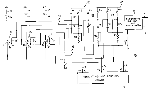
DESCRIPTION OF THE PREFERRED EMBODIMENT
Before describing the indicating and control cir-
cuit of the invent~on, it is helpful to review the oper-
ation of a circuit interrupter 10 such as depicted in
Figure 1. An electronic trip unit and power supply 11,
such as that described within aforementioned U.S. Patent
4,58S,052, is electrically connected through a sensing
circuit 12 with the separate phases of a three-phase
power distribution circuit consisting of conductors 13-
15 each of which contain a pair of separable contacts as
generally indicated at 16-18, respectively. Three cor-
responding current transformers 19-21 are arranged for
sensing the current through the individual phases by
means of a primary w;nding 22-24 which current is
reflected through transformer cores 25-27 and secondary
wind;ngs 22'-24' to the sensing circuit via wire conducN
tor pairs 28, 29 and 30, as indicated. The sensing
circuit 12 includes three bridge rectifiers 31, 32, 33
consisting of diodes Dl-D12 and three corresponding
burden reSistorS R1-R3. The equivalen~ volta~e value
for each phase of the phase conductors 13-15 obtained
across the burden resistors is ~ransmitted to the elec-
tronic trip unit and power supply 11 over conductors 34,
35 as well as to an indicating and control circuit 9
over conductors 5-7. This Yoltage information is pro-
cessed within the electronic trip unit and a decision isreached with respect to a circuit interruption function
therein. The indicating and control circuit provides a
-Yisual indication of the occurrence of a long-time over-
current condition as well as supplying output signals
for controlling the shut-down sequence of loads elec-
trically connected with the phase conductors.
; The indicating and control circuit 9 is depicted in
Figure 2 and is described as follows. The input termin-
als A-C receive the maximum representation of the indi-
`il
,
`" :1321822
vidual phase currents and compares the maximum against a user
adjustable reference within three inverting. Operational
amplifiers 36-38. The signal voltage obtained from the
sensing circuit for each phase, is applied to t~e amplifiers
through dropping resistors R4-R6 and to the double-diodes
39-41 connected respectively to the outputs of the
operational amplifiers through feedback resistors R7-Rg. The
double-diodes are type BAW 56 switching diodes obtained from
; Siemens. Capacitors Cl-C3 are used to filter out any
extraneous AC signals. The three-phase voltage signals
supplied to the inputs of the amplifiers are compared within
the double-diodes and the maximum phase signal voltage
appears across a single resistor R1o. The double-diodes are
matched pairs which serve to both compare the maximum voltage
and, by placing half of the diodes in the feedback loop, do
not affect the incoming voltage. The value of R1o is
selected to be equal to the individual resistors R7-Rg in
order that all the currents through the double-diodes will be
balanced. The voltage value appearing across Rlo is applied
to one input of a fourth amplifier 42, connected as a
comparator, through resistor R16 wherein it is compared to a
reference voltage value appearing across the resistance
bridge consisting of resistors R11-Rl3 ~hich is connected to
the other input of the fourth amplifier. The resistor R15
performs a positive feedback function to stabilize the com-
parator by adding hysteresis. The hysteresis determines the
time lag bet~een the "ON" and "OFF" states of the amplifier
and hence of the relay itself. The fourth amplifier is
adjusted such that the reference voltage applied to the
negative input can be set from approximately seventy percent
to ninety percent of the circuit breaker current rating.
When the ma~imum phase voltage signal exceeds the reference,
the amplifier turns on the indicator LED D13 to provide
visual indication that a predetermined long-time overcurrent
': ~
~2~2
- 6 --
condition has occurred. The indicator LED ~s connected
through a resistor R14 to a solid sta~e relay 43 which
includes a second LED D14 and a pair of photo-contacts
44. When the second light-emitting diode becomes trans-
missive, the photo-contacts respond to thereby provide
an isolated, conductive path bletween terminals T1, T2.
When the circuit interrupter 10 of Figure 1 is used with
sensiti~e manufacturing equipment, of the type described
earlier, a plurality of such solid state relays can be
arranged to selectively shut-down the equipment in a
predetermined manner. The arrangement of such a plural-
ity of solid state switches performs a "load-shedding"
function whereby selected equipment is shut-down while
the rest of the equipment remains operational until the
overcurrent condition ceases or until the electronic
trip unit times out the long-time overcurrent condition
and provides a trip signal over conductor 4 to open the
contacts 16-18 (Figure 1).
In load-shedding applications, the selection of the
hysteresis value that determines the time lag between
the "ON" and "OFF" states of the warning relay is criti-
cal. Hysteresis is normally used in amplifier circuits
to stabilize operation and prevent oscillation. As the
amplifier inputs approach a state change, a small amount
of such positive feedback ensures that the state change
takes place. Normally, the amount of hysteresis is
small, less than 1X, and the amplifier essentially
changes state at the same ~alue in both directions, that
is, " high" to "low" or "low" to "h~gh". When used to
implement an energy management funct~on directly, system
~- hysteresis!, rather than amplifier hysteresis is import-
ant, If the warning relay hysteresis were equivalent to
only 1X of the circuit breaker rating, a change in load
of more than 1X at the switch point will cause the relay
to change state. ~hen the warning relay operates at
.. ,
~ 3~2~2
70~, for example, removal of any load greater than lX
will cause the relay to change state again. The result
w;ll be rapid ON - OFF cyclinçl of the load, which pre-
sents an unstable system cond~ltion. By sett~ng the
hysteresis in the warning relay to a much higher value,
such as 10~, a sizable load can be removed without the
relay changing state until the remaining load reduces in
value. This is accomplished by selecting the proper
value of the resistor Rls of the amplifier 42. At the
IO same time, the actual load on the protected circuit can
be reduced by nearly IOX or the amount of the hystere-
sis. Figure 5 shows the system effect of hysteresis for
an 80% warning setpoint and a 10X hysteresis. The
arrows indicate the direction of operation ;n each
region. In the range between 70X and 80X of current
rating, the relay switch point is controlled by the
circuit breaker current without hysteresis as indicated
by the unidirectional arrows.
The c;rcult interrupter 10 of Figure 3 operates in
a manner similar to that o~ Figure 1. In this arrange-
ment, however, "peak" current is sensed across a single
burden resistor R16 rather than across a separate burden
resistor for each phase such as resistors R1-R3 in Fig-
- ure 1. Still referring to Figure 3, the current through
the phase conductors 13, 14, 15 is sensed by means of
current transformers 45, 46, 47 each of which includes a
primary winding (48-50), a secondary winding (54-56) and
a core (51-53). One side of each of the secondary wind-
inqs is connected in common to a conductor 65 while the
other side of the secondary windings is connected by
means of conductors 67-68 to bridge rectifiers 57, 58,
59 consisl:ing of diodes Dls-D22. The output of the
rectifters is applied to burden resistor R16 and to the
input of the electronic trip unit and power supply 11
over conductors 69, 70 which provides a trip output
~'~2~1 ~2~
-- 8 --
signal over conductor 4 in the manner described earlier
with reference to Figure 1. The voltage signal appear-
;ng across the burden resistor R16 is applied to the
negative input of an inverting amplifier 71 through
resistor R17. The negative input of the ampl~fier is
connected to the output in a feedback loop consisting of
feedbdck resistor R1g and diode D23. The operation of
the amplifier is similar to ~hat of amplifiers 36-38
shown earlier in Figure 2. The output of the amplifier
is peak-detected by capacitor C4 and applied through
resistor R1g to the positive input of a comparator 72
which includes a resistor R20 as a positive feedback
for hysteresis. This combination creates a track-and-
hold amplifier. A resistor bridge consist~ng of resis-
tors R22-R24 supplies a reference voltage to the nega-
tive input of the amplifier which is adjustable from
approximately seventy percent to 100X of the circuit
breaker current rating. When the reference voltage is
exceeded, a voltage signal appears at the output of the
second amplifier and is applied through a step-down
resistor R21 to a light-emitting d~ode D13 to give an
indication that the electronic trip unlt 11 is beginning
to time out a long-time overcurrent condition. As des-
cribed earlier, a solid state relay 43 consisting of a
light-emitting diode D14 and photo-contacts 44 are used
to provide electrical continuity between terminals Tl,
T2 to allow for selective switching between the electri-
cal loads connected within the protected circuit.
Figure 4 depicts an alternative sensing circuit 64
similar in several respects to that described earlier
with reference to Figure 2. The voltage representation
~A-~C of the individual phase conductors 13, 14, 15 of
Figure 1 is applied to terminals A, B, C and from there
; through dropping resistors R4-R6 to similar amplifiers
36-38 which contain similar resistors R7-Rg in a feed-
.
-
- ., ~. . . . ~ ,. .. .
~ ~ 2 ~
g
back loop arrangement. The double-diodes 39-41 of Fig-
ure 2 are replaced by RMS-to-DC converters 60-62 and
diodes D24-D26 wh~ch connect to the input of a special
amplifier 42'. One such RMS-to-DC device is an AD536A
sold by Analog Devioes, Inc. The burden resistor R1o is
connected to the positive inpult of the amplifier 42'. A
similar resistance bridge cons;isting of resistors R11-
R13 is connected to the negatllve input terminal to set
the reference value. The light-emitting diode D13 con-
nected to the output of the amplifier connects to thesolid state relay 43 through resistor R14. The light-
emitting diode D14 responds in a similar manner to close
the photo-contacts 44 and thereby allows current trans-
fer between terminals T1, T2 to operate the selected
loads as described earlier with reference to Figure 2.
An inexpensiYe indicating and control circuit has
herein been described for application with electronie
type circuit interruption de~tces. 80th RMS and peak
sensing circuits can ~e employed to indicate to an oper-
ator the occurrence of a long-time pick-up and can auto-
matically institute the shut-down of selected equipment
in a predetermined manner.
.
.