Note: Descriptions are shown in the official language in which they were submitted.
1321976
This invention relates to an apparatus for
forming a thin film, and more particularly, to an
apparatus for forming a compound thin film in which
the compound thin film is deposited on a substrate by
means of reactive ionized cluster beam method (R-ICB
method).
Conventionally, a compound thin film such as
TiN, A12O3, or SiC and the like, is coated on the
surface of a substrate by sputtering, chemical vapor
deposition (CVD) or the like. In using these appara-
tuses, however, there were problems in that the thin
film coated on the surface of the substrate had
insufficient hardness and low adhesive strength with
the substrate. For solving these problems, the
reactive-ionized cluster beam (R-ICB) method has been
developed, in which the thin film is formed by emit-
ting the vapor of a material to be deposited into a
reactive gas atmosphere by the use of the cluster ion
beam method.
A typical R-ICB apparatus is disclosed, for
example, in Japanese Patent Publication No. 57-54930
or Proceedings of the International Ion Engineering
Congress (ISIAT '83 and IPAT '83).
The present invention has been achieved in
order to solve the problem of the prior art.
.. . : .
: ,, . . ~ : ; . :
~ ' :` ,:;;': ~
- 1321976
It is a first object of the present inven-
tion to provide an apparatus for forming a thin film,
wherein an excimer laser beam emitting means emits
; excimer laser beams toward the neighborhood of a
' substrate, whereby increasing the reactivity of the
reactive gases in the vicinity of the substrate, that
is, activate the reactive gases, to make a chemical
reaction among the reactive gases and a vapor of a
material to be deposited, a cluster and a cluster ion
progress under the condition that the reactivity is
.
i~ remarkably high, whereby forming a thin film of a
;~ compound as the material to be deposited at a still
higher deposition speed and high efficiency.
. It is a second object of the present inven-
j~`;.
tion to provide an apparatus for forming a thin film,
. wherein a reactive gas activation means in addition to
` the excimer laser beam emitting means is provided,
, ..
whereby still more activating the reactive gases to
~ form the thin film of the compound as the material to
-`~ 20 be deposited at a high deposition speed and high
efficiency.
.~ It is a third object of the present inven-
';i tion to provide an apparatus for forming a thin film
which is capable of separately controlling a collision
speed against the substrate of the reactive gases and
. ,:
~ the material to be deposited, whereby controlling the
.
;.: A
-,` ~1
13~197~ :
quality, such as crystallinity and adhesion, of the
thin film.
The above and further objects and features
of the invention will more fully be apparent from the
following detailed description with accompanying
drawings.
The present invention is more readily
apparent from the following detailed description of a
preferred embodiment thereof when taken in conjunction
with the accompanying drawings, in which:
Fig. 1 is a schematic view showing a conven-
tional R-ICB apparatus; and
Fig. 2 is a schematic view of an apparatus
for forming a thin film on a substrate according to
the present invention.
In Fig. 1, an evacuation system 5 evacuates
gases in a vacuum chamber 6 and maintains the pressure
in the chamber 6 at a predetermined value. A reactive
gas supply means 4 for supplying an inside of the
vacuum chamber 6 with reactive gases comprises a gas
cylinder 41 for supplying reactive gases such as
oxygen, nitrogen and hydrocarbon into the chamber 6, a
flow regulation valve 42 for regulating the flow rate
of the reactive gases which are supplied from the gas
cylinder 41 to the chamber 6, and a gas introduction
pipe 43 for introducing the reactive gases to a
A
` ;
. . , . . . ~ .
- . , ....
, ` `,
. . , i ,.. ..
.
13~1 9~6
predetermined portion in the chamber 6. A vapor
generating means 1 for generating a vapor of a mate-
rial to be deposited comprises a closed type crucible
12 having a nozzle 11, wherein a material 15 to be
deposited is packed, a coiled filament 13 disposed
around the crucible 12 for heating the crucible 12 to
evaporate the material 15 therein, and a heat shield-
ing plate 14 for shielding the heat of the filament
13. Vapor of the material 15 is emitted out through
the nozzle 1] of the crucible 12 to form clusters 16
consisting of a large number of atoms. The clusters
16 formed are ionized by an ionization means 2 which
comprises an electron beam emitting means such as a
coiled filament 21, an electron beam extraction
electrode 22 for extracting electrons from the fila-
ment 21 and accelerating them, and a heat shielding
plate 23 for shutting out the heat of the filament 21.
A first acceleration electrode 3 disposed over the
ionization means 2 accelerates the ionized clusters
16a by means of its electrical field, so as to give
more kinetic energy to the ionized clusters 16a.
Disposed over the first acceleration electrode 3 is a
substrate 7 on whose surface a compound thin layer 71
is to be formed. An electric power unit 8 for the
vapor generating means 1 is provided on the outside of
the chamber 6 and it contains direct current power
A
.. . ..
.. , ~, .
.. . .. - .. . ` . ... ... ~ .. .
.. - ~ . ... . . . - .. ... ` ` . -
. .- ; . ` ~ . . . - -
. .
.. .. .
132~976
sources 81, 82 and 83 for giving a bias voltage and
power sources 84 and 85 for heating the filaments 13
and 21. Each of the bias power sources in the power
unit 8 functions as follows. The first direct current
power source 81 biases the potential of the crucible
12 positive in respect to the filament 13 so that
thermoelectrons emitted from the filament 13, heated
by using the power source 84, collide with the cru-
cible 12. The second direct current power source 82
biases the potential of the filament 21, heated by the
power source 85, negative in respect to the electrode
22, thereby drawing the thermoelectrons emitted from
the filament 21 into the inside of the electrode 22.
The third direct current power source 83 biases the
potentials of the electrode 22 and the crucible 12
positive in respect to the first acceleration elec-
trode 3 which is at an earth potential, so as to
control the acceleration of the positive charged
cluster ions by means of the electrical field lens
formed between the electrode 22 and the electrode 22.
The conventional R-ICB apparatus, con-
structed as mentioned above, operates as follows.
After evacuating the chamber 6 by the evacuation
system 5 to a pressure of around 1 x 10 6 mmHg, the
reactive gases are introduced into the chamber 6
through the pipe 43 by opening the valve 42. A
.
~321976
portion of the reactive gases supplied the inside of
the chamber 6 is activated, namely, excited or dis-
sociated, at a location above and near the vapor
genexating means 1. Then, this portion of the re-
active gases thus partially activated reaches the
surface of the substrate 7.
On the other hand, the crucible 12 is heated
by a collision of the electrons emitted from the
electrical field generated by the filament 13 to which
direct current is applied by means of the power source
81. By heating of the crucible 12, the material 15 in
the crucible 12 is vaporized to emit the vapor there-
from through the nozzle 11 into the chamber 6. At
this time, the crucible 12 is heated up to a tempera-
ture where the vapor pressure of the material 15 in
the crucible 12 reaches several mmHg. When the vapor
emitted from the crucible 12 passes through the small
nozzle 11, the clusters 16 are formed by adiabatic
expansion of the vapor due to the pressure differences
between the crucible 12 and the chamber 6 under
supercooling conditions. The clusters 16 are massive
atomic groups formed of condensed 100 to 1000 atoms of
the material 15 under the above conditions. A portion
of the clusters 16 are then ionized by the electrons
emitted from the filament 21 to make the cluster ions
16a. The cluster ions 16a are accelerated by the
; . . ~ ~: :: . .
.
, .. .
, ,: . . .
13219~6
electrical field generated by the first acceleration
electrode 3 to drift toward the substrate 7 along with
non-ionized clusters 16. Therefore, the substrate 7
is surrounded by the reactive gases introduced into
the chamber 6. Then, the reaction of the cluster ions
16a and clusters 16 with the reactive gases occurs in
the vicinity of the substrate 7 to produce compounds.
A thin film 71 of the compounds produced are then
deposited on the substrate 7.
In the above-mentioned conventional appara-
tus for the chamber 6 are in a molecular state and the
activity thereof is low. Moreover, since the reactive
gases activated around the vapor generating means 1
have short activity spans, the activated reactive
gases near the substrate 7 are apt to return to a low
activity condition. Therefore, the reactivity of the
compounds formed by the reaction is low, making the
thin film deposited on the substrate 7 unstable.
Further, most of the reactive gases are discharged
without being used to form the thin film of the
compounds.
The present invention is described in detail
with reference to a presently preferred embodiment
thereof as illustrated in Fig. 2. In Fig. 2, the same
reference numerals as in Fig. 1 indicate the same or
corresponding parts.
~ A
`
., ~ ~ .. ; . -.
132~ 976
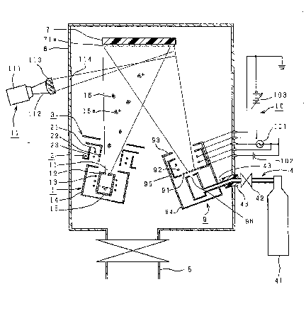
In Fig. 2, an internal vessel 94 is disposed
in a
A
.. , . . , ..... .. .. ` '
. ..... . .
.. . . .
.:
. . . , ~... . i. .
1321976
vacuum chamber 6 in a spaced opposite relation to a
substrate 7. A reactive gases activation means 9 for
ac'tivating, namely exciting, dissociating or ionizing,
reactive gases in the vicinity of the substrate 7, comprises
an internal vessel 94 and several members within the vessel
94 which will be described in detail later. The reactive
gases may be at least one of oxygen, nitrogen and
hydrocarbon or may contain elements which produce compounds
of a thin film to be deposited on the substrate 7. The
reactive gases are introduced into the vacuum chamber 6
through a gas supply means 4 and jetted therefrom into the
internal vessel 94 from a gas jet nozzle 96. The gas jet
nozzle 96 is connected with the inner end of a pipe 43 which
extends through and is hermetically mounted on a side wall
of the chamber 6 through an insulating member 45 formed of
ceramic. As electron beam emitting means 92 in the form of
a filament is disposed around a path of the reactive gases
which are jetted from the gas jet nozzle 96. An electron
beam extraction means 91 in the form of an electrode is also
disposed in and around the path of the jetted reactive gases
for extracting the electron beams from the filament 92. By
mean of the electrode 91 and the filament 92, the reactive
gases are activated with their electron beams. A shielding
means 95 in the form of a conductive plate such as a metal
plate for shielding potentials of the filament 92 and the
:~ .
' ' ': : ,
.
132~976
electrode 91 is disposed in the internal vessel 94 so as to
surround the filament 92 and the electrode 91. A second
acceleration electrode 93 for accelerating the jetted
reactive gases is disposed on an open end of the internal
vessel 94 in the jet direction of the reactive gases. The
internal vessel 94 surrounds the above-mentioned members,
namely, the filament 92, the electrode 91, the second
acceleration electrode 93 and the shielding means 95, and
the gas jet nozæle 96 disposed in the internal vessel 94.
These members comprise the reactive gases activation means
9.
An electric power unit 10 for the reactive gases
activation means 9 is provided on the outside of the chamber
6, which includes a power source 101 for heating the
filament 92, a direct current power source 102 for biasing
the electrode 91 to a positive potential in reæpect to the
filament 92 and the electrical shielding means 95, and a
direct current power source 103 for biasing the electrical
shielding means 95 and the electrode 91 to a positive
potential in respect to the second acceleration electrode
93.
The excimer laser device 111 for emitting the excimer
laser beam is disposed outside of the vacuum chamber 6.
Since this excimer laser beam has a short wave length, it is
suitable for the activation of the reactive gases.
'; '': ~ '
~ ' ~
~. :
1321976
The exc;mer laser beam 112 emitted from the excimer
laser device 111 is collected by the collection lens 113 and
then passed through the window 114, which is disposed on the
wall surface of the vacuum chamber 6 and formed of a
transparent plate provided with an air-tight sealing member
disposed along the periphery thereof, to be emitted toward
the neighborhood of the substrate 7. The excimer laser beam
emitting means 11 comprises the above described parts.
A vapor generating source 1 for generating vapors and
clusters of a material to be deposited, and other members,
namely, an ionization means 2 for ionizing the vapors and
clusters generated, and a first acceleration electrode 3 for
accelerating the ionized vapors and clusters are constructed
in the same manner as in Fig. 1 showing a conventional R-IC~
apparatus. In the embodiment of the present invention,
however, the crucible 12 has one nozzle 11 or several
nozzles. An illustration of an electrical power unit 8 for
the vapor generating means 1 is omitted in Fig. 2.
In the above-mentioned apparatus for forming a thin
film according to the present invention, the pressure in the
vacuum chamber 6 ls adjusted to be a predetermined degree of
vacuum by means of the evacuation system 5. The reactive
gases, flow rate of which is regulated by a flow regulating
valve 42, are introduced into the chamber 6 through a gas
introduction pipe 43. Then, the reactive gases introduced
.
- ~
1321~76
are further guided into the internal vessel 94 from the gas
elt nozzle 96, so as to adjust the pressure in the chamber 6
to be at about 10 to 10 mmHg. At this time, the gas
pressure in the internal vessel 94 is adjusted to be higher
than that of the chamber 6. The filament 92 as the electron
beam emitting means, disposed in the electrical field
shielding means 95, is heated to a temperature of about
~000~ by means of the power source 101. The power source
102 biases the electrode 91 to a positive potential in
respect to the filament 92 and the shielding means 95,
thereby emitting the electron beam from the filament 92
toward the electrode 91, which is disposed downstream of the
gas jet nozzle 96. By the application of the bias voltage
due to the power source 102, electrons of lA (ampere) to 5A
(amperes) are emitted from the filament 92 toward the
reactive gases jetted from the gas jet nozzle 96.
And, the extracted electrons are brought into collision
with molecules or atoms of the reactive gases in the
vicinity of the gas jet nozzle 96 to lead the reactive gases
to the condition that the molecules or atoms are excited
until the energy state is higher than the ground state, the
molecules are dissociated to the atomic state, or electrons
of the molecules or atoms are brought into collision to be
lost, whereby being ionized to activate.
In addition, simultaneously, the excimer laser beam 112
.
``
i32~976
from the excimer laser device 111 is emitted toward thc
neighborhood of the substrate 7 through the collecting lens
11~ and the window 114, whereby the reactive gases in the
vicinity of the surface of the substrate 7 are excited,
dissociated or partially ionized to reach the remarkably
activated state by the activating action of the laser beam
having a short wave length. In addition, although the
activation by the excimer laser beam 112 is possible for
both the reactive gases and the cluster 16, a still larger
energy is requlred for the activation of the cluster 16, so
that the activation of the reactive gases is mainly brought
about.
Since the potential of the filament 92 is identical to
that of the shielding means 95, the electron beams thus
emitted are confined within the shielding means 95 and are
especially concentrated around the path of the reactive
gases. Therefore, the reactive gases can be activated
efficiently to cover the substrate 7. The ionized reactive
gases and the electron beams are accelerated by the second
acceleration electrode 93 so as to im~inge against the
substrate 7. This acceleration can be controlled by varying
the voltage applied to the electrode 93. For example,
acceleration voltage of 0 to 0.2 KV causes about a 10 A/mm'
electron beam to irradiate the substrate 7 and 0.2 KV to 0.6
KY causes a 10 to 10~ AJmm ion beam to irradiate the
12
, ~
- 132197~
substrate 7.
On the other hand, in the vapor generating means 1, the
crucible 12 is heated to a temperature where a vapor
pressure of the material 15 to be deposited in the cruc;ble
12 becomes several mmHg, by means of the filament 13 to
which AC voltage is applied from the power source 84. In
this state, the heated material 1~ in the crucible 12 is
evaporated, and then emitted through the nozzle 11 to form
the clusters 16. A part of the emitted clusters 16 and
vapors are then ionized by electrons emitted from the
filament 21. The ionized vapors and the ionized clusters
16a are accelerated by an electrical field, which is
generated by the first acceleration electrode 3 under the
application of ~ to several K~ by the power source 83, so as
to impinge against the substrate 7 along with the remaining
non-ionized vapors and clusters 16.
On the other hand, the reactive gases, which have been
excited, dissociated and ionized by the excimer laser beam
112 and the reactive gas activation means 9, exist on the
substrate 7 and in the vicinity of the substrate 7 and
impinge against the vapour of the material to be deposited
15, the cluster 16 and the cluster ion 16a to make the
reaction progress, whereby forming the deposited thin film
71a of compound on the substrate 7. This activation leads
to an increased reactivity of the reactive gases and the
.
132197~
chemical reaction among the reactive gases, the vapour of
the material to be deposited 15, -the cluster 16 and the
cluster ion 16a makes progress at a remarkably high
activity, so that the deposited thin film of compound can be
formed at a high deposition speed and high efficiency.
At this time, it is possible to independently control
the kinetic energies of the reactive gas ions and the vapor
or cluster ions 16a by changing the application voltages to
the first and second acceleration electrodes 3 and 93
separately. This makes it possible to control the
properties of the compounds, for example crystalline
properties such as single crystal, polycrystal, mixed
crystal and amorphous, electrical properties, and adhesion
to the substrate.
As this invention may be embodied in several forms
without departing from the spirit of essential
characteristics thereof, the present embodiment is therefore
illustrative and not restrictive, since the scope of the
invention is defined by the appended claims rather than by
the description preceding them, and all changes that fall
within meets and bounds of the claims, or equivalence o
such meets and bounds thereof are therefore intended to be
embraced by the claims.
~ .
:,
,
'~' ` `, :
.