Note: Descriptions are shown in the official language in which they were submitted.
1322~33
~ower Amplifier For A Radio FreouencY Sianal
~i8 invention provides a power ~mpl~fier ~or
amplifying a r~dio freguency ~ignal, for ex~mple ~ pulsed
power ~mplifier responsive to a control pulse. The
amplifier i particularly useful for digit~l ~obile
cellular radio transmitters for use on the Pan-European GSM
lo cellular n~twork.
~ n a bur6t modulated power nmplifier, the
tran~mltter ~ust observo a time domain template upon
turn-on and turn-off, ~G well as a frequency domain
template. In the pa~t, th~ ~hape of the pow~r
characteristic as it rise6 ~t the ~tart of a burst and
fall~ at the end has been ~ontroll~d by mean6 of Ahaping
circuits con~i~ting of resistor~ and ~nalog cw~tch~s. Such
circuit~ can be bulky and unr~liable end have limited
accur~cy.
As well a~ the above power/time characteri6tic, the
output power of ~ GSM mobile r dio transmitter must be
~d~u~table in ~lxteen 6teps from +43 dbm to +13 d~m. Nany
tolerance f~ctors within the amplifier will af~ect the
ultimate output power. Manual ad~ustment mean~ can ~e
provided for pre-~etting the output power levels before the
~quipment lqaves the factory, howsver separate ~d~u3tment
~eans within the Qquipment for ~ach of the sixtsen power
levels would be ~ulky, and their ~d~u6tment would be t~me
con~uming.
It is an ~im of the pr-sent invention to prov~de an
i~proved power amplifier to overcome some o the ~bove
problems.
~*
1322~33
-- 2 --
According to t~e inventlon, a
power ampl~fier 16 prov~ded ~or amplifying a r~dio
~requency ~ignal, said amplifier c~mprlEing: power
celection means ~or select$ng n n~minal output power level
from a plurAlity of dl~crete levels; pow~r control ~-anc
for controlling output power ln response to sald power
~el~ction meanfi; input ~eans for lndicating me~ur-d outpu~
power; and ~torage means respon~lve to the input ~ean~ for
~toring in~ormation ~n respons~ to the ~easured output
power, for future adjustment of the ~electsd nominal output
power level. The information ~tored may be ~n indication,
$n respect Gf each of said nominal output power level~, as
to which Or ~ plurality o~ ~ub-l~vel~, offset from ~aid
selected level, gives ri6e to an output powex closest to
that nomin~l output power level.
In thi~ manner, whichever of the ~ub-level~ best
representing the desired output power level iB ~elected.
AB an altern~tive to providing preprogrammed ~ub-levels,
preprogram~ed or dynamic of~6et~ c~n be u~ed, which are
1322~33
- 3 -
~dded to the nsminal power level values. No manual
adju6tment i6 reguired. The ~torage mean~ record~ which of
S the ~ub-levels (or what off6et) i5 to be used and that
6ub-level tor off6et) iB u~ed thereafter. The remaining
4ub-levels xem~in unused. Thi~ f~cilitates calibr ting of
the power levels before the e~uipment leaves the factory.
It also ~akes recalibration Or the equipment guick and
6imple. With modification, recalibrat$on ~ould be carried
out ~utomatichlly by the equipment lt6elf. It al~o ~llows
for dynamic power control by changinq from one ub-level to~
enother (or ~y changing the of~6et) during use to
co~pen~ate for drift, temperature etc. The ~torage ~eans
~ay record, from one time ~lot to ~nother, ~n ~ndication of
the measur2d output power ~o as to control the output power
~n a later time-~lot.
The ~spect of the $nv~ntion can
oonveniently be implemented in a 6ingle 6haping ~OM. For
~xample, for sixteen level6, ach having four ~ub-levelc,
the ROM merely ha6 to ~tore 6ixty-four power/ti~e
characteristic~.
Preferably a ~eedback control loop is provi~ed
comprising senslng means for 6ens1ng output power and
co~parator ~e~ns ~or receiving and comparing an output
power sisnal from ~aid sensing means and an output power
level determining s~gnal, wherein 6aid power control meanR
are arranged to control the output power BO as to eguallse
aid ~gnal~. Whereas a diq~tal comparison ~subtraction)
¢ould be made, it is preferred that said comparator moans
ar~ arranged to receive ~aid output power ~ignal on a first
~nput and ~aid power determining signal on a second $nput,
said inputs being connected to a common voltage level by
means of tws diodes, 6aid diodes being ad~acent ach other
in 6ub~tantially isothermal relationship. I~ this ~anner,
var~ations in thermal characteristics of the diode detector
are e~fectively canoelled out. In the preferred
embodiment, the output power level determining signal i8
dertved via a digital-to-analog converter from the ~haping
1322~33
- 4 -
ROM, and the feedback ~ignal $~ derived from the output of
the power amplifier.
A preferred embodiment of the invention will now be
described with reference to the accompany$ng drawings, in
which:
Figure 1 shows a power amplifier for a radio
transmitter, in accordance with the present invention:
Figure 2 is a block d~agram showing the power
~mplifier
o~ Figure 1 during calibration of power levels;
Figure 3 shows a typical desired signal on ~eedback
loop 13.
Figure 4 shows a circult for use ~n an alternative
embodi~ent of the invention; and
Figures 5 ~nd 6 6how further circuits for use in
alternative embodiments of the invention, incorpDrating a
variable time base.
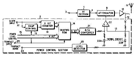
Referring to Figure 1, ~n RF ~ection 1 i~ shown and
a power control section 2. ~he RF 6ect~0n has an input 3
for receiving data to be transmitted ~nd an output 4 for
providing an RF signal ~or transmission. The RF signal is
fed to attenuator 9 and ~F power ampli~ier 10. The output
of power amplifier 10 is fea to the antenna 11. From the
output of the power ampl~fier 10, thare is also ~ level
6ensor 12, which is connected to a feed~acX loop 13 in the
power control secti~n 2.
The power cDntrol ~ction 2 has a six-bit power
control input 15, which i8 connected to the address lines
o~ a Ehaping RON 16. The power oontrol section 2 also has
a clock input 17, which is f~d to a six-bit counter 18
which in turn i8 connected to n further six ~ddress bits of
the ~haping ROM 16. ~ ramp control un~t 19 i8 connected to
the input Or the six-bit counter 18 ~nd is controlled by
the clock 17 and a transmit input 20. ROM 16 provides an
~ight-bit output which is fed to a digital-to-analog
converter 21, fro~ which the resulting analog signal is fed
via comparator amplifier 22 to the ~ttenuator 9 of the
1322~33
- 5 -
power amplifier 6ection 1. The negative input of
comparator amplifier 22 i6 connected to the level ~ensor 12
~ia the feedback loop 13. Each of the inputs of the
comparator amplifier 22 has a biasing diode 23a and 23b,
connecting it to ground. The diodes 23a and 23b are in
close thermal contact on the 6a~e chip. This ~eature has
the advantage of eliminatinq tha thermal coefficient of the
diode detector. A tran~mit-6ense line 24 i8 provided,
leading from the output power level sensor 12, via a level
detector 25 to the transmit controller 30 tFigure 2)
The operation of the ~mplifier is as follows.
The transmitter transmlt6 at a freguency from
890-915 NHz and receives at a frequency 45 MHz higher. The
transmitter is active for approximately one time slot in
every frame. A frame is 4.615 ms long and consists of
eight time slots. The time slot duration is 577 U8, which
i6 156.25 bits. The transmitter is active for only 147
bits or 543 us.
To transmit, the transmit controller 30 6elects a
power level on power level control lines 15, provides a
transmit control pulse on line 20 and provides data to be
transmitted on input 3. The output power template, i.e.
the output power/time characteri6tic, i~ controll~d by
counter 18, ramp control 19 and 6hap~ng ROM 16. When the
transmit key 20 indicates start of transmiss$on (S - Figure
3), ramp control 19 controls ~tart of ramping, whereupon it
counts 64 pulses (or 60me other number) to terminate
ramping. When the transmit key lndic~tes end of
transmls~ion (E), ramp control 19 causes counter 18 to ramp
down again through a different set of values. As the
transmit pulse progresses, counter 18 counts the input
clock pulses 17 and addresses ROM 16 accordingly. Thus,
for ~ given nominal power level, R~M 16 dict~tes the output
characteristic and the output power i6 controlled
~ccordingly by means of digital-to-analog converter 21,
comparator 22 and attenuator 9. For a different nominal
power level, a different characteristic is addressed by
132~33
- 6 -
~eans of dif~erent addresses on powex control input 15.
The ~ix power level control bit6 at input 15 ~erve
to ease the achievement of correct output power levels.
There are sixteen nominal power level6 and each nominal
power level is ~plit into four 6ub-level~ close to the
nominal value. Periodically, the tran~mit controller
carries out an output power test, during which it 6ets the
power to all the 64 possible power output values in turn.
The corresponding output powers are measured by external
power measuring means in the form of calibratlng apparatus
31. The transmit controller i~ then told by me~ns of an
input 32 which of the sub-level6 i~ the b~st to represent
2ach one of the ~ixteen nsminal output power levels. The
result i~ ~tored in ~torage means in the transmit
controller 30. Thereafter, the actual output power level~
will be correct.
The characteristic stored in the shaping ROM is an
approximation to a raised cosine. By this mean , the power
up/down ramp is slowed down, in order to reduce the
~pectral noise in adjacent channels due to the burst
modulation. The degree of approximation to the cosine is
limited by the step nature of the characteri~tic 6tored in
the ROM 16.
The above description has been g~ven by way of
exa~ple only, and modification of detail can b~ made within
the 6cope of the invention. Thus, for instance, the power
template6 stored in ROM 16 could be ~ub-divided into ~ewer
or ~ore time divi6ions by decreasing or increaeing the
clock rate 17 and selecting the count ratio of counter 18
accordingly. Likewise, fewer or more power ~ub-levels
oould be provided, and the number of power level control
line6 lS and capacity of ROM 16 would need to be 6elected
accordinqly. ~ikewise, greater or lesser accuracy can be
achieved from ROM 16 by providing more than aight bitC or
les~ than eight bits to the digital-to-analog converter 21.
~ he above features of sampling rate variation and
re601ution could be adapted to, or made a function of,
1322~33
different power levels or other parameters.
The power amplifier i~ not 601ely applicable to
QPSK transmitters, nor even to burst modulated
transmission. The mplifier could be used in radio
transmitters ~ther than for the GSN network, for example in
two-way radio. Thus, for power level control of a
continuous signal, counter 18 and ramp control 19 can be
omitted, leaving a much reduced ROM 16, wAich merely 6tores
the power levels for the four 6ub-level6 of each of the
sixteen nominal power level6. Similarly, for control of a
burst modulated tran6mission at a ~ingle power level, power
level control lines 15 could be omitted.
The output power i~ ad~ustable in 16 fitep6 from the
+43 dbm to ~13 dbm.
To avsid generating ~tep noise and glitches
potentially arising from digital ~teps in power level, a
simple integrator can be used to convert a step input into
a 610pe that i6 linear with r~pect to time. Usunlly,
however when an integrating amplifier is operating at a
~upply rail, it i8 610w in responding, and also the
negative input is not at virtual ground, enabling some
coupling of the input to the output. Figure 4A shows the
use of a pair of back-to-back zener diode~, Zl and Z2, that
will limit the output to plus or minus the zener voltage,
and keep the input at virtual ground. This circuit
generates ramps that are determined solely by Rl and Cl and
the input amplitude.
Figure 4B ohows a ~ircult in which the effectiva
value of Rl i5 modulated (by 6electively switching R2-R5
into parallel connectlon with Rl) and Cl and the input
amplitude are held constant. Ths input signal is derived
from a CMOS gate of negligible resi6tance ~compared to Rl),
~nd thu~ of constant amplitude (+6 to ground). ~he
positive input of the operatio~al amplifier 40 i6 biassed
to half of the CMOS voltage, 80 that the input ~wing
relative to the virtual ground is 6ymmetriral~ The output
will 6wing from this reference up approximately Zl volts
1322~33
-- 8 --
and down approximately Z2 volts, (plus a little more due to
~orward diode drops). For the purposes of describing the
operation, the Xey 6ignal enters at ~ 74Hc04, which, from a
logic input, produces a step from +6 volts Off to ground On
and back to ~6 volts at turn-off. Rl-Cl develops a very
gentle ramp, 60 that ~ust before a ~tep i6 to be executed
the output will be on a r~il. R2-R5 are ~11 lower value
r~sistors than Rl, in the ratio 8:4:2:1, 60 that in
combination o~ one or more, will develop fifteen different
net values of resistance against which Cl can work to
develop ramp6 o~ different 610pes, and are ~witched æo as
to modulate the ~lope of the output wave$orm.
There are many ways to generate the 610pe
~witching. For purposes of expl~nation, ~ progr~mmable
arr~y logic (PAL) $or a common table looX-up and count
control is employed. An oscillator provides a clock $ast
~nough to provide a multipla of pul6es to an up/down
counter during a ramp. It will advance the counter until
the table look-up reaches a prescribed count, at which
point ~he table cuts off further counting until key-down is
6ensed, at which time the counter will count down. The
counter's state i8 combined with the key signal in the PAL
to provide a translation to ~lope, 60 that the ~lope
profile can be di~ferent for key-up ~nd key-down, and need
not dwell equally on each slope in~rement, or indeed even
use all of the 15 increments available in thi~ embodiment.
Indeed, it may even be desirAble to us~ more than four
~witched resistors ~of binade ratio) or use some other
ratio.
The PAL al80 provides a test override so that
during testing, external signals hAve control o~ ~he
~lope. These ~re arranged 50 that if no external s~gnals
are conneoted when the test input is grounded, the 610pe
will be maximum. Slope maximum 18 use$ul in determining
the proper ~alue $or Cl.
The embodiment o$ Figure 4 ~s capable o~ generating
a ~moother transition with f~wer 6teps than the embodiment
1322~33
g
of Figure 1.
Figure 5 illustrates a further embodiment of the
,invention. In this embodiment, a high rate digital clock
50 feeds a v~riable modular counter 51, which, when keyed
down, divides by 1 or 2, thus providing a hlgh r~te clock
having
3electable clock rates to ~ binary r~mp counter 52. The
~0 counter 52 is locked from counting until key-up (point S in
Figure 3). The counter feeds a digital-to-nnalog converter
53, the filtered output of which controls the RF power
level. The D/A converter also feeds a modulo translatlon
table 54, which e6tablishes how many digital clocks ~re
required to advance the bi~ary ramp counter 52 by one
step. A controlling microcomputer 55 loads the modulo
translation table 54 with the desired ramp up and down
information for all the ~teps, ~ncluding key-up transmit
time and key-down. Upon a start command (to key up the
transmitter), the counter S2 6teps off. The period of each
step thereafter becomes a function of the translation.
As a practical matter, the digital clock 53 must be
faster that the desired ramp sp~ed. A 50 M~Z clock could
usually provide about 100:1 time ba6e to a r~mp in the
10-50 microsecond range. An alternative method would use a
VCO 60 as depicted in Figure 6, c~ntrolled by a linear D/A
converter 61 driven from the translation table 64. The
range of the VC0 m~ght be expanded by mixing and offsetting
it. For example a VC0 spanning the range 50-60 MHZ mlxed
against a 49 MHZ signal will y~eld 1-11 MHZ, moro linearly
than could easily be generated from a 1-11 MHZ VC0
directly.
Inatead of controlling attenuator 9 with the signal
from comparator 22, a power amplifier with variable gain
oontrol can be used and the signal from comparator 22 can
adjust the gain.
Temperature measuring means may also be provided,
and a further look-up table responsive thereto for
generating a temperature compensatins power offset 6ignal
1322~33
-- 10 --
to ~djust the output power to compen6ate for temperature
change6.
It will, of cour6e, be understood that the above
description has been given by way of example only and that
modifications of detail can be made within the ~cope o~ the
lnvention.
.~