Note: Descriptions are shown in the official language in which they were submitted.
1322~
SPECIFICATION
TITLE OF THE INVENTION
Television Signal Processing Apparatus
BACKGROUND OF THE INVENTION
1. Field of the Invention
The present invention relates to a television signal
processing apparatus which is capable of transmitting video
signals having a different aspect ratio from that of the
existing television systems, while being compatible with the
existing television systems.
2. Description of the Prior Art
In Japan, over 20 years have passed since the color
television broadcast under the existing NTSC (National
Television System Committee) system started in 1960. During
that period of time, various new television systems have
been proposed in response to the needs of a high definition
picture and due to the improvements of performance of
television receivers. The contents of TV programs
broadcasted have been changed from mere studio-made programs
or relay programs to programs providing images of high
pictorial quality which make impressions of a presence of an
actual scene, such as the cinema-sized broadcasting of
movies.
The specifications of the existing television
broadcasting are as follows: the number of saanning liens:
525, interlace scanning, luminance signal horizontal
bandwidth: 4.2 MHz, aspect ratio: 4:3 (cf., i.e. a
publication on the broadcast technology, title "Color
Television" edited and issued by The Japan Broadcasting
Corporation (NHK) 1961) When a movie is put on the air, the
.L~
,,
~322~
picture size of the movie must be adapted to the aspect
ratio of 4:3 of the existing television receivers by cutting
both sides of the movie picture or by providing dead spaces
on the upper and lower regions of a tube face so that the
aspect ratio of the usual picture area will correspond to
the value of the movie.
As described above, there lies a problem that when a
movie or a picture from which one may receive impressions of
an actual presence in a scene is televised under the
existing broadcast system, a part of the picture is to be
cut or the area of the picture must be reduced, thereby
failing to convey a complete message of the producer. A
mere transmission of signals having a larger aspect ratio
than that of 4:3 would disable the ordinary TV sets from
receiving said signals in a normal manner. With the number
of scanning lines and the frame frequency being equal to
those of the existing broadcast system, in order to obtain
the same hori20ntal resolution, the video bandwidth which is
m/4 times bigger than that of the existing aspect ratio is
required with respect to the aspect ratio of m:3 (m is an
actual number larger than 4). However, in view of the
effective utilization of electric wave resources, it i9
impossible to widen a transmission band in a disorderly
manner.
BRIEF DESCRIPTION OF THF DRAWINGS
Fig. 1 is a block diagram of the television signal
processing apparatus at the transmission side in accordance
with one embodiment of the present invention.
Figs. 2 and 3 are block diagrams showing one example`of
the internal configuration of the signal generator of Fig.
1.
Fig. 4 is a block diagram of the television signal
l322a~
processing at the reception side in accordance with one
embodiment of the present invention.
Figs. 5, 6, 7, 8, 9, 10, and 11 are block diagrams
showing the internal structure of the signal processing
circuit 111 of Fig. 4.
Fig. 12(a) is a spectral view showing a television
signal amplitude-modulated for vestigial side band in the
existing television system.
Fig. 12(b) is a spectral view of a band limited signal
modulated by a signal other than the signal as shown in Fig.
12(a), as one embodiment of the prior art.
Fig. 12(c) is a spectral view showing a multiplexing
between the signal of Fig. 12(b) and the signal of Fig.
12(a)-
Figs. 13(a)-13(e) are views of signal waveforms showing
the courses of processing of signals in the form of the
time-axis compression and time-axis expansion.
Figs. l~(a)-14(e) are views showing in spectrum the
signal waveforms of Figs. 13(a)-13(e).
A number of methods are here considered for widening
the aspect ratio while remaining compatible with the
existing television system. For example, when an original
picture is picked up with an aspect ratio of m:3 which has a
larger frame size than the conventional one, firstly the
video signals are time-axis expanded by m/4 times which
correspond to the portion appearing on the tube face of the
existing television receiver with the aspect ratio of 4:3.
In order to obtain information of picture area with an
aspect ratio of m:3, among the remaining portions of the
video signals, the low frequency component will be
transmitted by way of time-axis multiplexing and the high
frequency component by non-time-axis multiplexing that is,
~ Sl
1322~
multiplexing methods such as quadrature modulation or
frequency interleaving or other methods which are not
time-division multiplexing methods. Figs. 12(a)-12~c) are
spectrum views showing a non-time axis multiplex processing
method of one embodiment of the prior art. Fig. 12(a) is a
spectrum view of a television signal amplitude-modulated for
a vestigial side band. Fig. 12(b) shows a multiple signal
other than the television signal as shown in Fig. 12(a),
wherein the multiple signal is a modulated version for a
vestigial side band of a carrier P2 which is same in
frequency as carrier Pl but out of phase therewith Fig. 12(c)
shows a multiplexing of the signal of Fig. 12(b) and the
signal of Fig. 12(a). The bandwidth of the multiple signal
is not restricted to this.
As for the method for non-time-axis multiplex
processing, there is a method wherein multiplexing takes
place in the first and third quadrants which are positions
conjugate to chrominance sub carriers on the
temporal-vertical two-dimensional frequency plot.
However, there was no clear and concrete indication of
how the luminance and chrominance si~nals of the video
signals as well as the time-axis will be processed in such
methods.
SUMMARY OF THE INVENTION
An object of the present invention is to provide a
television signal processing apparatus which is compatible
with the existing television system and serves to produce
television signals having a large aspect ratio.
For the purpose of attaining the above-described
object, the present invention provides a television signal
processing apparatus at the transmission side comprising a
,~
~ ~ 2 ~
signal producing block adapted to perform time-axis
compression, time-axis expansion and chrominance signal
processing of an electrical signal obtained from an original
received picture and having an aspect ratio larger than the
standard one, so as to thereby produce a main signal and a
multiple signal, and a non-time-axis multiplexing block for
multiplexing the main signal and the multiple signal.
Furthermore, the present invention provides a
television signal processing apparatus at the reception side
comprising a non-time-axis multiplexed signal separation
block for separating said multiplexed signals, a block for
separating a luminace signal and a chrominace signal, a
block for demodulating the chrominance signal, a block for
effecting time-axis compression, a block for expanding on
time-axis the signal multiplexed on time-axis, and a block
for compressing on time-axis the non-time-axis multiplexed
signals.
The foregoing structure enables production of
television signals which are capable of, while compatible
with the existing television system, transmitting in a
multiplexing manner picture information having an
aspect ratio larger than the standard one. A TV receiver
constructed for the intended purpose can receive without
difficulties picture images of the conventional television
broadcast by means of the time-axis compression on one hand
and obtain pictures having a larger aspect ratio than
conventional by use of the synchronous detection, time-axis
compression, time-axis expansion, etc. Even a TV receiver
of the conventional type but provided with said structured
device may receive pictures of the conventional television
broadcast without difficulties.
.~
132204~
DESCRIPTION OF THE PREFERRED EMBODIMENTS
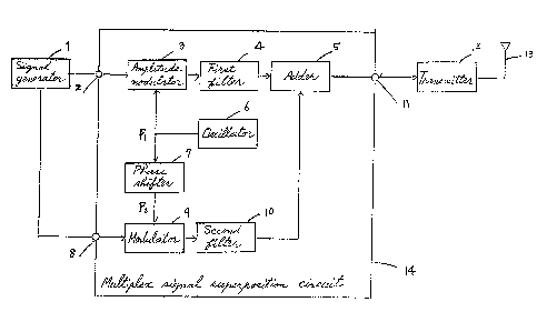
Fig. 1 is a block diagram of a television signal
processing apparatus at the transmission side in accordance
with one embodiment of the present invention. In this
drawing, element 1 is a signal generator; element 2 is a
main signal input terminal; elament 3 is an amplitude
modulator; element 4 is a first filter; element 5 is an
adder; element 6 is an oscillator; element 7 is a phase
shifter; element 8 is a multiplex signal input terminal;
element 9 is a modulator; element 10 is a second filter;
element 11 is a composite signal output terminal; element 12
is a transmitter; element 13 is an antenna, and element 14
is a multiplex signal superposition circuit.
The signal generator 1 serves to produce a main signal
and a multiplex signal. The main signal is inputted from
the main signal input terminal 2 to the multiplex signal
superposition circuit 14. The multiplex signal is inputted
from the multiplex signal input terminal 8 to the multiplex
signal superposition circuit 14. The main signal inputted
into the multiplex signal superposition circuit 14 is used
by the amplitude modulator 3 to amplitude-modulate a carrier
Pl obtained from the oscillator 6. The obtained amplitude
modulation wave is band-limited by the first filter 4 to
turn into a vestigial side band before being input to the
adder 5. The carrier P1 obtained from the oscillator 6
shall be a modified version called "carrier P2" when the
phase of the former has been shifted by the phase shifter 7.
When the outputs of the first and second filters 4 and 10
are added together by the adder 5, the phases of the
carriers are shifted so that they will intersect one another
at right angles. The carrier P2 is amplitude-modulated at
its double side band by the modulator 9, using a multiplex
, 6
, "~
~322~
signal inputted into the multiplex signal superposition
circuit 14 for carrier suppression, preferably at least for
a blanking period. After being band-limited by the second
filter 10, the output of the modulator 9 is input to the
adder 5. The output from the adder 5 will be a composite
signal. The composite signal will be transmitted by the
transmitter 12 through the antenna 13. The frequency
characteristic of the second filter 10 here shall possess a
characteristic feature as shown in Fig. 12(b).
Fig. 2 is a block diagram showing one example of the
internal configuration of the signal generator 1 of Fig. 1.
Element 21 is an input terminal for a luminance signal Y
obtained from a picture signal taken by a camera having for
example, an aspect ratio larger than the usual aspect ratio;
element 30 is an input terminal for a chrominance signal I
obtained from said picture signal; element 3~ is an input
terminal for a chrominance signal Q obtained from said
picture signal; elements 24, 26, 33, 35, 41, and 43 are
time-axis expansion circuits; elements 25, 34, and 42 are
time-axis compression circuits; elements 27, 36 and 44 are
switches; elements 22, 31, and 39 are LPFS (low-pass
filters); element~ 23, 32, and 40 are HPFs (high-pass
filters); elements 28 and 46 are adders; elements 37 and 45
are balanced modulators; element 29 is a main signal output
terminal, and element 47 is a multiplex signal output
terminal.
The signal corresponding to the portion formed on the
screen of a television receiver shall be referred to as a
first signal, and other signal, e.g. the one corresponding
to the both sides or one side, shall be referred to as a
second signal. The luminance signal Y obtained through
known matrix circuits from a signal into which the images
7 -
~ 3 2 ~
have been converted by a camera having a larger aspect ratio
than the usual one is, for example, inputted into the
time-axis expansion circuit 24, and LPF 22 and HPF 23.
If an original picture is taken with a large aspect
ratio of m:3, the first signal corresponding to the portion
formed on the screen of a usual TV set will be time-axis
expanded by m/4 time by the time-axis expansion circuits 24,
33, 41. With the CCD camera requiring a shorter
horizontal blanking period than a camera tube, it is not
always necessary to time-axis expand the signal
corresponding to the portion formed on the screen of the
usual television set.
The luminance signal has on the time axis a waveform as
shown by Fig. 13(a) by way of example, while on the
frequency axis is represented by a low spectrum distribution
by the energy of high frequency component as a general
characteristic of the picture signal ~See Fig. 14(a)). The
luminance signals of the ~econd signal corresponding to the
portion of the opposite sides or one side of the screen are
divided by the LPF 22 and HPF 23 into a low frequency
component of high energy (the waveform of Fig. 13(b) and
frequency spectrum of Fig 14(b)) and a high frequency
component of comparatively low energy (the waveform of Fig.
13(d3 and frequency spectrum of Fig. 14(d)) to be delivered
to the time-axis compression circuit 25 and the time-axis
expansion circuit 26 respectively. In the time-axis
compression circuit 25, as illustrated by Fig. 13(c), the
low frequency component as shown in Fig. 13(b) is time-axis
compressed to such a degree that the latter will turn into a
frequency spectrum which may occur below the band
transmissible by the NT5C system. The resultant low
frequency component is fed to the switch 27, where it and
,~ 8 -
1322~
the output of the time-axis expansion circuit 24 are
time-axis multiplexed together. In the time-axis
compression circuit 25, time adjustment is carried out so
that the time-axis compression signal will be time-axis
multiplexed during at least part of an overscanning period
for electron beams or a part of the front porch in the
period of the horizontal blanking.
The general receiver overscans electron beams on the
order of 8% of the usual picture area. Consequently, if
the time-axis compressed signals are timely adjusted during
the period corresponding to, for example, 2% of said
percentage and 2% of the usual picture area of the front
porch so that the time-axis compressed signals will be
time-axis multiplexed, then no time-axis multiplex signal
will affect the reproduced images of the usual TV receivers.
The adjustment of the time-axis may be performed by delaying
signals using memory, for example. The time-axis expansion
and time-axis compression may be achieved by, for example,
changing write clocks and read clocks of a memory.
In the time-axis expansion circuit 26, the hi~h
frequency component as shown in Fig. 13(d) is time-axis
expanded as shown in Fig. 13(e) to such an extent that it
will be positioned below the bands where the band can be
non-time-axis multiplex. Signals which are band-compressed
by means of time time-axis expansion circuit 26 are inputted
into the adder 46.
Chrominance signals I and Q are similarly processed.
For example, the chrominance signals I and Q obtained from
signals into which visual images have been converted by a
camera having a larger aspect ratio than the usual one are
inputted into the time-axis expansion circuits 33 and 41,
LPFs 31 and 39, and HPFs 32 and 40 respectively. When an
,~. _ g _
original picture image is received with an aspect ratio of
m:3 (i.e.-a picture width greater than that of the
conventional image), the first signal corresponding to the
visual spot appearing on the screen of the usual TV set is
time-axis expanded by m/4 times by the time-axis expansion
circuits 33 and 41 as in the case of the luminance signal Y.
The chrominance signals I and Q of the second signals
corresponding to the regions of the both sides or one side of
the picture tube are separated by the LPFs 31 and 39 and the
HPFs 32 and 40 into a low fre~uency component of high energy
and a high frequency component of comparatively low energy
respectively, and the both components will be supplied to
the time-axis compression circuits 34 and 42 and the
time-axis expansion circuits 35 and 43. The time-axis
compreRsion rate, time-axis expansion rate and time-axis
ad;ustment are the same as in the case of the luminance
signal.
The signals time-axis compressed are fed to the
switches 36 and 44 respectively, where said signals are
time-axis multiplexed with the outputs of the time-axis
expansion circuits 33 and 41 respectively. The outputs of
the switches 36 and 44 are quadrature-modulated by the
balanced modulation circuit 37 and added to the output of
the switch 27 by means of the adder 28. The output of the
adder 28 will be a main signal.
The outputs of the time-axis expansion circuits 35 and
43 are quadrature-modulated by the balanced modulation
circuit 45 and added by the adder 46 to the outputs of the
time-axis expansion circuit 26. The output of the adder 46
will be a multiplex signal.
If the HPFs 32 and 40 are replaced by LPFs, then the
LPFs 31 and 39, the time-axis compression circuits 34 and 42
-- 10 --
.~
~322a4~
and the switches 36 and 44 may be omitted.
Fig. 3 iS a block diagram showing one example of the
internal configuration of the signal generator 1 of Fig. 1.
Element 51 is, for example, an input terminal for the
luminance signal Y obtained from signals into which images
have been converted by the camera with a larger aspect ratio
than the usual one; element 56 iS an input terminal for the
chrominance signal I obtained from said picture signal;
element 61 is an input terminal for the chrominace signal Q
obtained from said signal; elements 67 and 71 are time-axis
expansion circuits; element 68 is a time-axis compression
circuit; elements 54, 59, 64, and 69 are switches; elements
53, 58, and 63 are LPFs; elements 52, 57 and 62 are HPFs;
elements 55 and 66 are adders; 60 and 65 are balanced
modulation circuits; element 70 is a main signal output
terminal, and element 72 is an output terminal for the
multiplex signal.
For example, the luminance signals Y obtained from
signals into which received images have been converted by
the camera with a larger aspect ratio than the usual one
through a known matrix circuit are inputted into the switch
54, the LPF 53 and the HPF 52 respectively. When an
original picture image is picked up with a conventional
aspect ratio of m:3 having a greater frame width, the first
signal corresponding to the visual spot appearing on the
screen of a television set of the usual type is passed
through the switch 54 into the adder 55. The luminance
signals of the second signal corresponding to the spot(s) of
the opposite sides or one side of the screen are separated
respectively by the LPF 53 and the HPF 52 into a low
frequency component and a high frequency component so that
the both components will be supplied to the adder 66 and the
f~
1322Q'~
switch 54 respectively. During the period corxesponding to
the spot of the both sides or one side of the screen, the
output of the HPF 52 is passed through the switch 54 into
the adder 55.
The chrominance signals I and Q are similarly
processed. For example, the chrominance signals I and Q
obtained via the known matrix circuit from signals into
which visual images have been converted by a camera having a
larger aspect ratio than the usual one are inputted into the
switches 59 and 64, the LPFs 58 and 63 and the HPFs 57 and
62 respectively. The chrominance signals I and Q of the
first signals are passed through the switches 59 and 64
respecti~ely into the balanced modulator 60. The
chrominance signals I and Q of the second signals are
separated by the LPFs 58 and 63 and the HPFs 57 and 62 into
a low frequency component and a high frequency component.
The outputs of HPFs 57 and 62 are passed through the
switches 59 and 64 into the balanced modulator 60
respectively during the period corresponding to the spot of
the both sides or one side of the screen. The signals,
after being subjected to quandrature-modulation, are
inputted into the adders 55 and 66.
Among the outputs of the adder 55 the signals
corresponding to the spot appearing on the screen of a
usual television receiver are time-axis expanded by the
time-axis expansion circuit 67 and then inputted into the
switch 69. A time-axis expansion by m/4 times occurs in the
time-axis expansion circuit 67. All of the signals, except
for said signals, are time-axis expanded by the time-axis
expansion circuit 71. In said time-expansion circuit 71,
the high frequency component as shown in Fig. 13(d) is
time-axis expanded so that the band will be located under
- 12 -
~3~2~1
the bands where non-time-axis multiplexing may take place as
illustrated in Fig. 13(e). The outputs of the adder 66 is
time-axis compressed by the time-axis compression circuit 68
and inputted into the switch 69. In the time-axis
compression circuit 68, the low frequency components shown
in Fig. 13(b) are time-axis compressed so that said low
frequency components will be a frequency spectrum which may
occur below the bands transmissible by way of NTSC system as
shown in Fig. 13(c), and then delivered to the switch 69
where it will be time-axis multiplexed. The output of the
switch 69 will be a main signal. The output of the
time-axis expansion circuit 71 will be a multiplex signal.
In the time-axis compression circuit 68, time adjustment
shall be held during the period of at least part of a period
where an over-scanning of electron beams is carried out in
the receiver, or part of the front porch of a period of the
horizontal blanking so that the time-axis compressed signals
may be time-axis multiplexed.
If the HPFs 57 and 62 are replaced by an LPF, then the
LPFs 58 and 63, the balanced modulator 65 and the adder 66
may be omitted.
Though blanking period signals such as synchronization
signals or burst signals have been omitted, reference
signals or identification signals may be multiplexed during
the blanking period. The reference signal may be construed
as a standard reference signal for correcting white signal
levels, black signal levels, amplitudes of chrominance
signals, phases, etc. or a control signal for controlling
regenerative carriers. The identification signal is, for
example, a signal for distinguishing said composite signal
from television signals for use in the existing
broadcasting.
- 13 -
~ 3 2 ~
Since the time-axis expanded signals are widened in
band by subjecting them to time-axis compression at the
reception side, even a larger aspect ratio will cause no
decrease of the resolution. Of the second signals
corresponding to information on the both sides or one side
of the screen face outside the frame of aspect ratio 4:3,
non-time-axis multiplexed signals are destined to be almost
erased by the synchronous detection with aide of a video
carrier in the usual TV receiving system in the event of the
intersection of the existing television with such spectrums,
whereby interference due to the non-time axis multiplex
signals will rarely occur. In the receiver for demodulating
multiplex signals, main signals can be taken out without any
quadrature distortion as in the existing receiver, and by
conducting a synchronous detection by a phase-controlled
video carrier and by use of a filter can be picked up also
non-time axis multiplexed signals corresponding to
informations of the both sides or one side of the screen
face outside the frame of aspect ratio 4:3 without
quadrature distortion involved. Also, the signals subjected
to time-axis multiplexing may be reproduced by a process
such as time-axis expansion. That is, the reproduction can
be provided of an original picture image having an aspect
ratio larger than 4:3 and received at the transmission side.
Next, the signal processing at the reception side in
accordance with one embodiment of the present invention will
be described. Reference will be made to the reception of,
for example, TV signals joined together by said signal
processing. Fig. 4 is a block diagram of the television
signal processing apparatus at the reception side in
accordance with one embodiment of the present invention. In
the drawing; element 101 is an antenna; element 102 is a
1,~..,
tuner; element 103 is a first filter; element 104 is a first
detector; element 105 is a carrier reproduction circuit;
element 106 is a second filter; element 107 is a phase
shifter; element 108 is a second detector; element los is a
main signal output terminal; element 110 is a multiplex
signal output terminal; element 111 is a signal processing
circuit, and element 112 is a demodulation circuit.
A signal produced at the transmission side is received
by the antenna ~01, and frequency-converted to the
intermediate frequency band by means of the tuner 102, and
band-limited by the first filter 103. Though the antenna is
specificaily shown, the transmission may also be by cable.
The band-limited signal is fed to the first detector 104 and
the carrier reproduction circuit 105, where a carrier I1
will be produced for synchronous detection. the synchronous
detection of the band-limited signal is carried out by the
carrier Il in the first detector 104. The output of the
first detector 104 shall be a main signal.
The output of the tuner 102 is band-limited by the
second filter 106. The band-limited signal is synchronously
detected in the second detector 108 by means of a carrier I2
which ha~ been shifted in phase from the carrier I1 and
which is obtained from the carrier reproduction circuit 105.
It is noted that the amount of phase shift of the carrier I2
should be consistent with that of the transmission side.
the detection output will be a multiplex signal. The main
signal and the multiplex signal are inputted into the signal
processing circuit 111. For the non-time-axis multiplexing
of multiplex signals, a method is considered wherein the
signals are multiplexed in first and third quadrants which
are conjugate positions to chrominance sub carriers in the
plane of the time-vertical frequency. With the signal
~32~Q4~
demodulated into a base band at the reception side, the
separation of the main signal from the multiplex signal may
be dependent on whether at least the phase of the
chrominance sub carrier takes up a difference of a signal
with which the chrominance sub carrier will be in phase or a
sum of a signal with which the chrominance sub carrier will
be opposite phase between the fields.
Fig. 5 is a block diagram showing one embodiment of the
internal structure of he signal processing circuit 111 of
Fig. 4. Element 121 is a main signal input terminal;
element 139 is a multiplex signal input terminal; elements
122 and 141 are YC separation circuits; elements 123 and 142
are chrominance demodulation circuits; elements 124, 126,
128, and 140 are time-axis compression circuits; elements
125, 127, and 129 are time-axis expansion circuits; elements
130, 132, and 134 are switches, elements 131, 133, and 135
are adders; element 13~ is an output terminal for luminance
signal Y; element 137 is an output terminal for chrominance
signal I, and element 138 is an output terminal for
chrominance signal Q.
The main signals inputted from the main signal input
terminal 121 are separated by the YC separation circuit 122
into luminance signals Yc and chrominance signals Cc. Among
the Yc signals which have been outputted from the YC
separation circuit 122, the signals corresponding to the
screen face of the existing television having an aspect
ratio of 4:3 and having been time-axis expanded at the
transmission side are time-axis compressed by the time-axis
compression circuit 124, while the other signals having been
time-axis compressed at the transmission side are time-axis
expanded by the time-axis expansion circuit 125. In the
time-axis compression circuit 124 and the time-axis
- 16 -
132~
expansion circuit 125, reverse time-axis processing and
time-axis regulation take place respectively to the
time-axis expansion and time-axis compression at the
transmission side so that the transmission and reception are
combined together to keep a normal time relationship.
The chrominance signals Cc from the YC separation
circuit 122 are demodulated by the chrominance demodulation
circuit 123 into Ic signals and Qc signals. As in the case
of the Yc signals, among the Ic and Qc signals, signals
which have been time-axis expanded at the transmission side
and corresponding to the region of the aspect ratio of 4:3
are time-axis compressed by the time-axis compression
circuits 126 and 128, while the other signals which have
been time-axis compressed at the transmission side are
time-axis expanded by the time-axis expansion circuits 127
and 129.
on the other hand, multiplex signals produced from the
multiplex signal input terminal 139 are time-axis compressed
by the time-axis compression circuit 140 and then separated
by means of the YC separation circuit 141 into luminance
signals Ys and chrominance signals Cs. the chrominance
signals Cs are demodulated by the chrominance demodulation
circuit 142 into Is and Qs signals. The luminance signals
Ys are added to the output of the time-axis expansion
circuit 125 by the adder 131 and then inputted into the
switch 130. In the switch 130, the output of the time-axis
compression circuit 124 will be produced during the
corresponding to the region of the aspect ratio of 4:3,
while the output of the adder 131 will be produced during
other periods.
Similarly, Is signals are added to the output of the
time-axis expansion circuit 127 by the adder 133 and then
inputted into the switch 132. In the switch 132, the output
- 17 -
~ 3220~
of time-axis compression circuit 126 will be produced during
the period corresponding to the region of the aspect ratio
4:3 and the output of the adder 133 will be produced during
other periods as chrominance signals I respectively.
Similarly, Qs signals are added to the output of the
time-axis expansion circuit 129 by the adder 135 and then
inputted into the switch 134. In the switch 134, the output
of the time-axis compression circuit 128 will be produced
during the period corresponding to the region of the aspect
ratio of 4:3 and the output of the adder 135 will be
produced during other periods as chrominance signals
respectively. The luminance signals Y, chrominance signals
I, and chrominace signals Q may be monitored after being
converted to R,G,B signals by a matrix circuit.
If chrominance signals are not superposed on signals
which have been time-axis multiplexed, then the time-axis
expansion circuits 127 and 129, and adders 133 and 135 are
not necessary, and so the outputs Is and Qs of the
chrominance demodulation circuit 142 may be inputted into
the switches 132 and 1~4 respectively.
To ensure that the existing television broadcast will
be received without difficulties, the time-axis compression
circuits 124, 126 and 128 are intended for restoring TV
signals by compressing portions, time-axis expanded, of said
TV signals having the aspect ratio with a greater frame
width. That is, in order that a visual image can be
received in conformity with the conventional aspect ratio,
it is necessary to time-axis compress the existing
television signals. Its compression ratio is dependent on
the aspect ratio used. However, in case a display means is
of a liquid crystal type which doesn't require as large a
blanking period as a CRT, the time-axis compression is not
- 18 -
132~
always necessary. In the reception of the existing
television signals, an image with the aspect ratio of 4:3
may be positioned near the central portion of the TV picture
tube, whereas the remaining portions of the picture tube
with an aspect ratio of a larger frame width are darkened by
blanking.
Fig. 6 is a block diagram showing one example of the
internal structure of the signal processing circuit 111.
Element 151 is a main signal input terminal; element 152 is
a multiplex signal input terminal; elements 153, 159, 166,
and 172 are switches; element 155 is a YC separation
circuit; element 162 is a chrominance demodulation circuit;
elements 154, 156, 163, and 169 are time-axis compression
circuits; elements 157, 164, and 170 are time-axis expansion
circuits; elements 160, 167 and 173 are adders; elements 158
and 165 are time-axis regulation circuits; element 161 is a
luminance ~ignal Y output terminal; element 168 is a
chrominance signal I output terminal, and element 174 is a
chrominance signal Q output terminal. Main signals from the
main signal input terminal 151 are inputted via the switch
153 to the YC separation circuit at the period of video
signals.
Multiplex signals from the multiplex signal input
terminal 152 are time-axis compressed at the time-axis
compression circuit 154 contrary to the time-axis
expansion at the transmission side and then, inputted via
the switch 153 to the YC separation circuit 155 at the
blanking period and then separated by the YC separation
circuit 155 into luminance signals Yl and chrominance
signals Cl. Among the Yl signals produced from the YC
separation circuit 155, signals corresponding to the picture
- 19 -
~ . . .
~:32~
tube face of the existing television receiver with the aspect ratio of
and time-axis expanded at the transmission side are time-
axis compressed by the time-axis compression circuit 156 and
other signals time-axis compressed at the transmission side
are time-axis expanded by the time-axis expansion circuit
157.
Subsequently, luminance signals obtained by separating,
in the YC separation circuit, the multiplexed signals
time-axis compressed, during the blanking period, are
adjusted at the time-axis regulation circuit 158 so as to
form a normal time relationship~ and then added to the
output of the time-axis expansion circuit 157 by the adder
160. The chrominance signals C1 produced by the YC
separation circuit 155 are demodulated by the chrominance
demodulation circuit 162 into Il and Ql signals. Of the Il
and Ql signals, as Yl signals, signals corresponding to the
portion of the aspect ratio of 4:3 and time-axis expanded at
the transmission side are time-axis compressed by the
time-axis compression circuits 163 and 169 respectively, and
other signals time-axis compressed at the transmission side
are time-axis expanded by the time-axis expansion circuits
164 and 170.
on the other hand, chrominance signals, obtained by
separating the multiplexed signals time-axis compressed, by
the YC separation circuit during the blanking period, are
demodulated by the chrominace demodulation circuit 162 into
I1 and Ql signals, regulated by the time-axis regulation
circuits 165 and 171, and added to the outputs of the
time-axis expansion circuits 164 and 170 by the adders 167
and 173 so as to form a normal time relationship. In the
switches 159, 166, and 172, the outputs of the time-axis
compression circuits 156, 163 and 169 will be produced at
- 20 -
~322~
the period corresponding to tha portion of the aspect ratio
of 4:3 and the outputs of the adders 160, 167 and 173 will
be produced at other periods as luminance signals Y,
chrominance signals I, and chrominance signals Q.
If the chrominance signals are not superposed on the
time-axis multiplexed signals, then the time-axis expansion
circuits 16~ and 170 and the adders 167 and 173 are no
longer required, and the outputs of the time-axis regulation
circuits 165 and 171 may be output to the switches 166 and
172 respectively.
As described above, in accordance with the circuit
structure of the present invention, the main signals and the
multiplexed signals can be processed in the same separate YC
separation circuit and chrominance demodulation circuit,
which provides a highly effective circuit structure.
Fig. 7 is a block diagram showing one example of the
internal structure of the signal processing circuit 111.
Element 181 is a main signal input terminal; element 199 is
a multiplexed signal input terminal; elements 182 and 200
are YC separation circuits; elements 183 and 202 are
chrominance demodulation circuits; elements 184, 186, 188,
201, and 203 are time-axis compression circuits; elements
185, 187, and 189 are time-axis expansion circuits; elements
190, 192 and 194 are switches; elements 191, 193, and 195
are adders; element 196 is a luminance signal Y output
terminal; element 197 is a chrominance signal I output
terminal, and element 198 is a chrominance signal Q output
terminal.
Main signals from the main signal input terminal 181
are separated by the YC separation circuit 182 into
luminance signals Yc and chrominance signals Cc. Among the
Yc signals to be outputted by the YC separation circuit 182,
21 -
".
~3~2~4~
signals time-axis expanded at the transmission side and
corresponding to the picture tube face of the existing
television set with the aspect ratio of 4:3 are time-axis
compressed by the time-axis compression circuit 184, and
other signals time-axis compressed at the transmission side
are time-axis expanded by the time-axis expansion circuit
185. The chrominance signals Cc produced from the YC
separation circuit 182 are demodulated by the chrominance
demodulation circuit 183 into the Ic and Qc signals
respectively. As with the Yc signals, among the Ic and Qc
signals, signals time-axis expanded at the transmission side
and corresponding to the portion of the aspect ratio of 4:3
are time-axis compressed by the time-axis compressed
circuits 186 and 188 respectively, and other signals
time-axis compressed at the transmission side are time-axis
expanded by the time-axis expansion circuits 187 and 189.
on the other hand, the multiplexed signals from the
multiplexed signal input terminal 199 are separated by the
YC separation circuit 200 into luminance signals Ys and
chrominance signals Cs, and then time-axis compressed by the
time-axis compression circuits 201 and 203 respectively.
The outputs of the time-axis compression circuit 203 are
demodulated by the chrominance demodulation circuit 202 into
Is signals and Qs ~ignals. The outputs from the time-axis
compression circuit 201 are added to the output of the
time-axis expansion circuit 185 by the adder 191, and then
inputted into the switch 190. In the switch 190, the output
of the time-axis compression circuit 184 will be produced at
the period corresponding to the portion of the aspect ratio
4:3, and the output of the adder 191 will be produced at
other periods as luminance signals Y respectively.
Similarly, Is signals are added to the output of the
- ~2 -
1`~
~2~
time-axis expansion circuit 187 by the adder 193, and then
inputted into the switch 192. In the switch 192, the output
of the time-axis compression circuit 186 will be produced at
the period corresponding to the portion of the aspect ratio
4:3, and the output of the adder 193 will be produced at
other periods as chrominance signals I respectively.
Similarly, Qs signals are added by the adder 195 to the
output of the time-axis expansion circuit 189, and then
inputted into the switch 194. In the switch 194, the output
of the time-axis compression circuit 188 will be produced at
the period corresponding to the portion of the aspect ratio
of 4:3, and the output of the adder 195 will be produced at
other periods as chrominace signals Q respectively. The
chrominance signals Cs as output signals from the YC
separation circuit 200 may be time-axis compressed after
demodulated, and then inputted into the adders 193 and 195.
If the chrominance signals have not been superposed on
the time-axis multiplexed signals, the use of the time-axis
expansion circuit 187 an 189 and the adders 193 and 195 is
not necessary, and the outputs Is and Qs of the chrominance
demodulation circuit 202 may be inputted into the switches
192 and 194 respectively. When the chrominance signals Cs
as the output signals ~rom the YC separation circuit 200 are
time-axis compressed after being demodulated, the signals
time-axis compressed may be delivered to the switches 192
and 194.
Fig. 8 is a block diagram showing one example of the
signal processing circuit 111 of Fig. 4. Element 221 is a
main signal input terminal; element 225 a multiplex signal
input signal terminal; elements 227 and 229 are YC
separation circuits; elements 228 and 230 are chrominance
- 23 -
~322~4~
demodulation circuits; elements 222 and 226 are time-axis
compression circuits; element 223 is a time-axis expansion
circuit; element 224 is a switch; elements 231, 232, and 233
are adders; element 234 is a luminance signal Y output
terminal; element 235 is a chrominance signal I output
terminal, and ~lement 236 is a chrominance signal Q output
terminal.
Among the main signals from the main signals input
terminal 221, signals time-axis expanded at the transmission
side and corresponding to the picture tube face of the
existing television receiver with an aspect ratio of 4:3 are
time-axis compressed by the time-axis compression circuit
222, and other signals time-axis compressed at the
transmission side are time-axis expanded by the time-axis
expansion circuit 223.
The multiplexed siqnals from the multiplex signal input
terminal are time-axis compressed by the time-axis
compression circuit 226. In the time-axis compression
circuits 222 and 226 and in the time-axis expansion circuit
223, time-axis processing and time-axis regulation are
reversed with respect to the time-axis expansion and
time-axis compression at the respective transmission sides,
so that transmission and reception are combined together to
keep a normal timing relationship. In the switch 224, the
output of the time-axis compression circuit 222 will be
inputted at the period corresponding to the picture tube
face of the existing television receiver with an aspect
ratio of 4:3, nd the output of the time-axis compression
circuit 226 will be inputted at the other period
respectively into the YC separation circuit 227. In the YC
separation circuit 227, separation into luminance signals Yc
and chrominance signals Cc occurs. The chrominance signals
- 24 -
1322~4~
Cc as being the output of the YC separation circuit 227 are
demodulated by the chrominance demodulation circuit 228 to
Ic and Qc signals.
on the other hand, the outputs of the time-axis
expansion circuit 223 are inputted into the YC separation
circuit 229 wherein they will be separated into luminance
signals Ys and chrominance signals Cs. The chrominance
signals Cs are demodulated by the chrominance demodulation
circuit 230 into Is and Qs signals. the luminance signals
Yc are added to the luminance signals Ys by the adder 231 to
form luminance signals Y. Similarly, the chrominance
signals Ic are added to the chrominance signals Is by the
adder 232 to form chrominance signals I. Similarly, the
chrominance signals Qc are added to the chrominance signals
Qs by the adder 233 to form chrominance signals Q.
If the chrominace signals are not in superposition on
the time-axis multiplexed signals, the use of the YC
separation circuit 229, the chrominance demodulation circuit
230 and the adders 232 and 233 is unnecessary, and the
output of the time-axis expansion circuit 223 may be
inputted into the adder 231. The output of the chrominance
demodulation circuit 228 will become chrominan¢e signals I
and Q.
This structure of circuit of the TV receiver may do
only with a single system in the time-axis compression
circuit ~or the multiplex signal, a time-axis expansion
circuit, and a time-axis compression circuit for the main
signal, which constitutes a necessary and minimum structure
of the time-axis processing circuit.
Fig. 9 is a block diagram showing one example of the
internal structure of the signal processing circuit 111 of
Fig. 4. Element 251 is a main signal input terminal;
- 25 -
13~2~
element 255 is a multiplex signal input terminal; element
257 is a YC separation circuit; element 261 is a chrominance
demodulation circuit; elements 252 and 253, and 256 are
time-axis compression circuits; elements 258, 262, and 265
are time-axis expansion circuits, element 254 is a switch;
elements 259, 263 and 266 are adders; element 260 is a
luminance signal Y output terminal; element 264 is a
chrominance siqnal I output terminal, and element 267 is a
chrominance signal Q output terminal.
Among main signals from the main signal input terminal,
signals time-axis expanded at the transmission side and
corresponding to the portion of the picture tube face of the
existing tele~ision receiver with an aspect ratio of 4:3 are
time-axis compressed by the time-axis compression circuit
252. Other signals time-axis compressed at the transmission
side are time-axis compressed by the time-axis compression
circuit 253, so that the time-axis adjustment will be made
as to allow the signals to appear within the blanking
period.
Multiplex signals from the multiplex signal input terminal
are time-axis compressed by the time-axis compression circuit
256. The switch 254 is operative to input into the YC separation
circuit 257 the output of the time-axis compression circuit 252
at the period corresponding to the picture tube face of the
existing television receiver with an aspect ratio of 4: 3, and to
input the output of the time-axis compression circuit 256 at
other imaqe signal periods, and to input the output of the
time-axis compression circuit 253 during the blanking period.
These inputted signals are separated by the YC separation circuit
257 into luminance signals Y1 and chrominance signals Cl. The
chrominance signals C1 output by the YC separation circuit 257
are demodulated by the chrominance demodulation circuit 261 to Il
signals and Q1 signals. ~mong the luminance signals Y1 output by
- 26 -
.,.,~
'Q!~
the YC separation circuit 257, the ones corresponding to thesignals which have been time-axis compressed by the time-axis
compression circuit 253 are time-axis expanded by the time-axis
expansion circuit 258 and time-axis adjusted so that a normal
time relationship will be realized. The other luminance signals
and the output of the time-axis expansion circuit 258 are added
to one another by the adder 259 to form luminance signals Y.
Similarly, among the chrominance signals Il output by the
chrominance demodulation circuit 261, chrominance signals I
corresponding to the signals time-axis compressed by the
time-axis compression circuit 253 are time-axis expanded by the
time-axis expansion circuit 262 and time-axis adjusted so that a
normal time relationship will be realized. The other chrominance
signals I are added to the output of the time-axis expansion
circuit 262 by the adder 263 to form chrominance signals I.
Similarly, among chrominance signals Q1 output by the
chrominance demodulation circuit 261, signals corresponding to
the signals time-axis compressed by the time-axis compression
circuit 253 are time-axis expanded by the time-axis expansion
circuit 265 to effect time-axis adjustment for establishing a
normal time relationship. The other chrominance signals Q are
added to the output of the time-axis expansion circuit 265 by the
adder 266 to form chrominance signals Q.
If the chrominance signals are not in superposition to the
signals time-axis multiplexed, the time-axis expansion circuits
262 and 265, and the adders 263 and 266 are not necessary, and
the outputs I1 and Q1 of the chrominance demodulation circuit 261
will become chrominance signals I and Q respectively.
Since the main signals and the multiplex signals are not
processed separately by the YC separation circuits and the
chrominance demodulation circuit, but by the same single
circuit, this structure could be an effective structure of
- 27 -
~:2:2 ~
receiver. Fig. 10 is a block view showing one example of
the signal pr~cessing circuit 111 of Fig. 4. Element 281 is
a main signal input terminal; element 282 is a multiplex
signal input terminal; element 286 is a YC separation
circuit; element 292 is a chrominance demodulation circuit;
elements 283 and 284 are time-axis compression circuits;
elements 287, 293, and 298 are time-axis expansion circuits;
elements 288, 294, and 299 are time-axis adjustment
circuits; elements 285, 289, 295 and 300 are switches;
elements 290, 296 and 301 are adders; element 291 is a
luminance signal Y output terminal, element 297 is a chrominance
signal I output terminal, and element 302 is a chrominance signal
output terminal.
The main signals from the main signal input terminal 281 are
time-axis compressed by the time-axis compression circuit 283.
On the other hand, the multiplex signals from the multiplex
signal input terminal are time-axis compressed by the time-axis
compression circuit 284, performing a time-axis adjustment to
avoid any superposition of the multiplex signals on the output
signals of the time-axis compression circuit 283 on a timing
basis. In the time-axis compression circuits 283 and 284,
the time-axis process is carried out in a reverse manner
with respect to the time-axis expansion at the transmission
side respectively, provided further time-axis compression
will be performed on the time-axis multiplexed signals. The
switch 285 is operative to input into the YC separation
circuit 286 the output of the time-axis compression circuit
283 at the period corresponding to the picture tube face of
the existing television receiver with an aspect ratio of 4:3
as well as at the period in which the time-axis multiplex
signals have been subjected to time-axis compression and
will input the output of the time-axis compression circuit
284 during other periods. The YC separation circuit 286
- 28 -
~322~
acts to separate these signals into luminance signals Y1 andchrominance signals C1. The chrominance signals Cl output
by the YC separation circuit 286 are demodulated by the
chrominance demodulation circuit 292 into I1 and Q1 signals.
Among the luminance signals Y1 from the YC separation
circuit 286, luminance signals corresponding to the time-axis
multiplexed signals are time-axis expanded by the time-axis
expansion circuit 287 to effect a time-axis adjustment for
establishment of a normal time relationship. Additionally, the
luminance signals corresponding to the multiplexed signals are
time-axis adjusted by the time-axis adjustment circuit 288 for
establishment of a normal time relationship. The addition of the
output of the time-axis expansion circuit 287 and the output of
the time-axis adjustment circuit 288 occurs in the adder 290.
The switch 289 is operative to select the output of the YC
separation circuit 286 at the period corresponding to the picture
tube face of the existing television receiver with an aspect
ratio of 4:3 and to select the output of the adder 290
during other periods. The output of the switch 289 will be
luminance signals Y.
Similarly, among the chrominance signals I1 output by the
ahrominance demodulation circuit 292, chrominance signals I
correspondin~ to the time-axis multiplexed signals are time-axis
expanded by the time-axis expansion circuit 293 and then
time-axis adjusted to establish a normal time relationship.
Also, chrominance signals I corresponding to the multiplexed
signals are time-axis adjusted by the time-axis adjustment
circuit 294 to establish a normal time relationship. The
addition of the outputs of the time-axis expansion circuit 293
and time-axis adjustment circuit 294 is performed by the adder
296. The switch 295 is operative to select the output of the
chrominance demodulation circuit 292 at the period corresponding
to the picture tube face of the existing television receiver with
an aspect ratio of 4:3 and to select the output of the adder
t~ 29
~322~4
2g6 during other periods. The output of the switch 295 will be
chrominance signals I.
Similarly, among the chrominance signals Q1 output by the
chrominance demodulation circuit 292, signals Q corresponding to
the time-axis multiplexed signals are time-axis expanded by the
time-axis expansion circuit 298 and then time-axis adjusted to
establish a normal time relationship. In addition, signals Q
corresponding to the multiplex signals are time-axis adjusted by
the time-axis adjustment circuit 299 to establish a normal time
relationship. The addition of the outputs of the time-axis
expansion circuit 298 and time-axis adjustment circuit 299 is
achieved by the adder 301. The switch 300 is operative to select
the output of the chrominance demodulation circuit 292 at the
period corresponding to the picture tube face of the existing
television receiver with an aspect ratio of 4:3 and to
select the output of the adder 301 during other periods.
The output of the switch 300 will be chrominance signals Q.
With no superposition of the chrominance signals on the
time-axis multiplexed signals, the time-axis expansion circuits
293 and 298 and the adders 296 and 301 are no longer
necessary, and the outputs of the time-axis adjustment
circuits 294 and 299 may be inputted into the switches 295,
and 300 respectively.
As described above, since the main signals and the multiplex
signals are not processed separately by the YC separation circuit
and chrominance demodulation circuit, but by the same single
circuit, this structure could be an effective circuit
structure.
Fig. ll i8 a block diagram showing one example of the
internal configuration of the signal processing circuit 111 of
Fig. 4. Element 321 is a main signal input terminal; element 334
is a multiplex signal terminal; elements 323 and 335 are YC
separation circuits; elements 324 and 337 are chrominance
demodulation circuits; elements 322, 336, 338 and 339 are
~f~ 30
13~.Q~
time-axis compression circuits; elements 325, 326, and 327 are
time-axis expansion circuits; elements 328, 330, and 332 are
switches; elements 329, 331, and 333 are a*ders; element 340 is a
luminance signal Y output terminal; element 341 is a chrominance
signal I output terminal, and element 342 is a chrominance signal
Q output terminal.
After main signals from the main signal input terminal are
time-axis compressed by the time~axis compression circuit 322,
the resultant signals are separated by the YC separation circuit
323 into luminance signals Yc and chrominance signals Cc. Some
of the Yc signals output by the YC separation circuit 323 are
time-axis compressed at the transmission side and then time-axis
compressed again by the time-axis compression circuit 322
before they are expanded by the time-axis expansion circuit
325 to be received by the adder 329. The chrominance
signals Cc output by the YC separation circuit 323 are
demodulated by the chrominance demodulation circuit 324 into
Ic and Qc signals. Similarly, the Ic and Qc signals are
time-axis compressed at the transmission side, and then by the
time-axis compression circuit 322 and then time-axis expanded by
the time-axis expansion circuits 326 and 327 until they are
inputted into the adders 331 and 333 respectively.
On the other hand, multiplex signals from the multiplex
signal input terminal 334 are separated by the YC separation
circuit 335 into luminance signals Ys and chrominance signals Cs.
The chrominance signals Cs are demodulated by the chrominance
demodulation circuit 337 into Is and Qs signals. The luminance
signals Ys are time-axis compressed by the time-axis compression
circuit 336, and then added to the output of the time-axis
expansion circuit 325 by the adder 329 and finally inputted into
the switch 328. The switch 328 is operative to output the
output Yc of the YC separation circuit 323 at the period
f~ - 31 -
13~2~4~
corresponding to the portion of the aspect ratio of 4:3 and
to output the output of the adder 329 during other periods,
both output signals being luminance signals Y.
Similarly, the Is signals are time-axis compressed by the
time-axis compression circuit 338, added by the adder 331 to the
output of the time-axis expansion circuit 326, and inputted into
the switch 330. In the switch 330, the output Ic signals of the
chrominance demodulation circuit 324 will be outputted at the
period corresponding to the portion of the aspect ratio of
4:3 and the output of the adder 331 will be outputted during
other periods respectively as chrominance signals I.
Similarly, the Qs signals are time-axis compressed by the
time-axis compression circuit 339, added by the adder 333 to the
output of the time-axis expansion circuit 327, and inputted
into the switch 332. In the switch 332, the output Qc
signals will be outputted at the period corresponding to the
portion of the aspect ratio of 4:3 and the output of the
adder 333 will be outputted during other periods
respectively as chrominance signals Q.
With no superposition of the chrominance signals on the
multiplex signals, the time-axis expansion circuits 326 and 327
and the adders 331 and 333 are unnecessary, and the outputs of
the time-axis compression circuits 338 and 339 may be inputted
into the switches 330 and 332 respectively.