Note: Descriptions are shown in the official language in which they were submitted.
~3~2~
BACKGROUND OF THE INVENTXON
ield of the Invention ,
The present invention relates generally to a
moving detection circuit and more particularly to a
moving detection circuit for generating a moving
detection signal which is utilized in a television
receiver such as a so~called improved definition
television receiver (IDTV) for providing an improved
image quality by using movement-adaptive type scanning
line interpolation or the like.
BRIEF DESCRIPTION OF THE DRAW NGS
FIG. 1 is a bloc~ diagram showing an example of a
prior art television receiver which has a moving
detection circuit;
FIG. 2 is a schematic block diagram showing an
example of a prior art moving detection circuit used
in the television receiver shown in FIG. l;
FIG. 3 is a schematic bl~ck diagram showing an
example of a prior art scanning line interpolating
ci.rcuit used in the television receiver show~ in FIG~
l;
FIG. 4 is a schematic diagram showing a scanning
line structure of the prior art scanning line
interpolating circuit from a time and vertical surface
standpoint;
FIG. 5 is a diagram of the spectrum showing a
frequency characteristic of a low-pass filter used in
a moving detection circuit of the present invention;
J
,~ .
~3222~1
-- 2
FIGS. 6A to 6D are respectively schematic
representations used to explain that the prior art
moving detection circuit i.~ normally operated when the
moving speed is low;
FIGS. 7A to 7D are respectively schematic
representations used to explain that the prior art
moving detection circuit is not normally operated when
the moving speed is high;
FIG. 8 is a block diagram showing an embodiment
of a moving detection circuit according to the present
invention;
FIG. 9 is a block diagram showing an example of a
tel~vision receiver to which the present invention is
applied;
FIG. 10 is a block diagram showing a signal
processing circuit which includes a second embodiment
of the moving detection circuit according to the
present invention;
FIG. 11 is a schematic diagram used to explain
the scanning line structure of the second embodiment
of the invention from a time and vertical surface
standpoint;
FIGS. 12A throuyh 12G are, respectively,
schematic diagrams used to explain the operation of
the second embodiment of the moving d~tection circuit
according to the present invention;
.
- . .
'' ~ '' ' :'
~ 32224~
-- 3 --
FIG. 13 is a block diagram showing a third
embodiment of the moving detection circuit according
to the present invention;
FIG. 14 is a schematic diagram showing a scanning
line structure in the third embodiment of the present
invention from a time and vertical surface standpoint;
FIG. 15 is a schematic diagram showing a scanning
line structure of time and vertical surface in the
vertical non-correlation mode of the third embodiment
of the moving detection circuit according to the
present invention;
: FIG. 16 is a block diagram showing a fourth
embodiment of the moving detection circuit according
to the present invention;
FIGS. 17A to 17H are respectively schematic
diagrams used to explain how the fourth embodiment of
the moving detection circuit of the present invention
is effectively operated to detect a high hand
component;
FIG. 18 is a schematic diagram of a scanning line
structure of time and vertical surface in the vertical
correlation mode of the fourth embodiment of the
moving detection circuit according to the present
invention from a phase relationship of high hand
: 25 component standpoint;
FIGS. l9A to l9C are respectively schematic
diagrams used to explain that high band components
. _~
: ~'
;
22~L~
-- 4
cancel each other out in the vertical corr~lation mode
in the fourth embodiment o~ the moving detection
circuit according to the present invention;
FIG. 20 is a schematic diagram of a scanning line
structure of time and vertical ~urface of vertical
non-correlation mode of the fourth embodiment of the
moving detection circuit according to the present
invention from a phase relationship of the high band
component standpoint; and
FIGS. 21A to 21C are respPctively sche~atic
diagrams used to explain that in the fourth embodiment
of the moving detection circuit according to the
present invention, the high band component causes a
detection error in the vertical non-correlation mod~.
Description of the Prior Art
; FIG. 1 is a block diagram showing an example of a
prior art television receiver.
Referring to FIGo 1~ a video signal is applied to
an input terminal 62 and is supplied to an analog-to-
digital (A/D) converter 63, where it is converted to a
digital video signal. The digital video signal is
then fed to a Y/C separating circuit 64, in which it
is separated to provide a luminance signal Y and a
chrominance signal C.
The luminance signal Y from the Y/C separating
circuit 64 is supplied to a scanning line
interpolating circuit 65Y. The chrominance signal C
,~
.
~ 3~2~
-- 5 --
from the Y/C separating circuit 64 is supplied to a
chroma decoder 66, where it is decoded to provide a
time-division signal of R-Y/B Y of red and blue color
difference signals R-Y and B-Y. ~he time-division
signal R-Y/B-Y from the chroma decoder 66 is supplied
to a scanning line interpolating circuit 65C. The
scanning line interpolating circuits 65Y and 65C
generate main scanning line signals Ym and Rm-Ym/Bm-Ym
in addition to the interpolating scanning line signals
Yc and Rc.~Yc/Bc-Yc simultaneously.
The luminance signal Y from the Y/C separating
circuit 6~ is supplied to a moving detection circuit
50. The moving detection signal from the moving
detection circuit 50 is supplied to a coeffisient
generator 51. The amplifying value K of the
multipliers in the scanning line interpolating
circuits 65Y and 65C is generated by the coe~ficient
generator 51, and the valu~ K changes in response to
the magnitude of th~ moving d~tection signal. For
example K = 0 for the still picture portion and the
maximum value of K is 1 for rapid movement.
The moving detection circuit 50 will be described
more fully with referQnce to FIG. 2.
Referring to FIG. 2, the luminance signal Y from
the Y/C separating circuit 64 (see FIG. 1) is supplied
to a series circuit comprising field memories 401 and
402 each of which form a delay line~ The delay time
`:
':
3 ,~
-- 6 --
of the series circuit of the field memories 401 and
402 is one frame (263H + 262H~.
The input signal to the field memory 401 and the
output signal from the field memory 402 are supplied
to a subtractsr 403, where they are subtracted from
each other. The frame difference signal ~rom the
subtracter 403 is supplied to a low~pass filter 404,
in which the high band noise component and the dot
interference component thereof are removed. The thus
processed signal from the low-pass filter 404 is
supplied to an absolute value circuit 405 where it is
converted to an absolute value. The output cignal
from the absoluke value circuit 405 is the moving
detection signal.
Japanese Laid-Open Paten~ No. 55-8124 discloses
the above techni~ue in which the moving detection
signal i5 detected from the same difference signal.
The scanning line interpolation circuit 65Y is
; constructed, for example, as shown in FIG. 3.
Referring to FIG. 3, the luminance signal Y
delivered from the Y/C separating circuit 64 (see FIG.
1) i5 supplied to a line memory 601 which forms a
delay line which has a delay time of lH (one
horizontal line period). The input and ou~pu~ signals
of the line memory 601 are supplied to an adder 602,
where they are added and averaged. The output signal
from the adder 602 is multiplied by K (K_l) by a
:
~3~22~1
multiplier 603, and is then fed to an adder 604.
The luminance signal Y from the Y/C separating
circuit 64 (FIG. 1) is also supplied to a field memory
605 which forms a delay line. Tne delay time of the
field memory 605 is selected to be 263H. The output
; signal from the field memory 605 is multiplied by(1 - K) by a multiplier 606, and is then fed to the
adder 604.
FIG. 4 shows a scanning line structure from a
time-vertical surface standpoint. In FIG. 4, an open
circle represents the scanning line of each field.
Assuming that h is the above-mentioned input signal,
that i is the outpu~ signal of the line memory 601 and
that i is the output signal of the field memory 605,
and these signals h to i are arranged to have a
positional relationship such as shown in FIG. 4.
: In the scanning line interpolating circuit 65Y,
the output signal h + i of the adder 602 is an
interpolating scanning line signal which represents
the real moving picture portion, whereas the output
signal i of the field memory 605 is the interpolating
scanning line signal which represents the still
picture portion. The adder 604 generates an output
which is an interpolating scanning line signal Yc in
which the interpolating scanning line signals of the
real moving picture and of the still picture portion
are added at a ratio corresponding to the amount of
~.
`'
~ 32~2~
-- 8
movement. The scanning line which is to be
interpolated is located as shown by a broken line
circle in FIG. 4.
The input signal h is directly utilized as the
main scanning line signal Ym.
The scanning line interpolating circuit 65C is
similarly constructed and is not described in detail.
Referring back to FIG. 1, the main scanning line
signals ~m and Rm-Ym/Bm-Ym and the interpolating
scanning line signals Yc and Rc-Yc/Bc-Yc from the
scanning line interpolating circuits 65Y and 65C are
supplied to timebase-compressing circuits 67Y and 67C,
respectively. The timebase-compressing circuits 67Y
and 67C time-compress each of the main scanning line
signals Ym, Rm-Ym/Bm-Ym and the interpolating scanning
line signals Yc, Rc-Yc/Bc-Yc by one hal~ respectively,
and the signals are sequentially generated. In this
case, the timebase-compressing circuit 67C generates
red and blue color difference signals, separately.
The double-speed luminance signal and color
diference signals from the timebase-compressing
circuits 67Y and 67C are supplied to digital to-analog
(D/A) converters 68Y, 68R and 68B, in which they are
converted to analog signals, respectively.
~he double-speed luminance signal and color
difference signals from the D/A converters 68Y, 6BR
and 68B are supplied to a matrix circuit 73. The
''~ ~
. ' .
~ 132~2~
g
double-speed red, green and blue signals R, G and B
from the matrix circuit 73 are respectively supplied
through amplifiers 74R, 74G and 74B to a color cathode
ray tube (color CRT) 75, where a color video signal
which has double the normal scanning lines is
displayed on the screen of the color CRT 75 according
to the non-interlaced scanning sy~tem.
The television receiver shown in the example of
FIG. 1 is disclosed, fox example, in NEC technical
report Vol. 41, No. 3/1988.
The chrominance signal component has a phase-
inverting relationship between the frames so that when
the luminance signal y contains the dot interference
component, the output signal of the subtracter 403
(FIG. 2) also contains the dot interference component.
In the moving detection circuit 50 shown in the
example of FIG. 2, when the low-pass filter 404 is
formed as a so-called COS filter which has a frequency
response characteristic which becomes lower around,
for example, 3.58 MHz (refer to a solid line curve a
i.n FIG. 5), movement of relatively high frequency can
be detected. There is, however, presented such a
problem in that the dot interference component
(chrominance signal component) contained in the output
signal from the subtracter 403 cannot be effectively
removed. When on the other hand the low-pass filter
404 is formed as a so-called COS2 filter which has a
'&~
: .
~.3%224~
-- 10 --
response characteristic which becomes lower around,
for example, 3.58 MHz (ref~r to a broken line curve k
in FIG. 5) t the dot interference component can
effectively be removed but the moving detection
ability so as to detect movement of a relatively high
frequency i5 deteriorated.
Further, in the moving detection circuit 50 shown
in FIG. 2, the frame difference signal is used as the
moving detection signal, and the moving detection is
performed during a unit of a frame frequency (1~30
second). There is then a problem because a quick
movement such as a field fre~uency (1/60 second~
cannot be detected, which fact causes a detection
error to occur. This will be described more fully
with reference to FIGC. 6A to 6D and FIGS. 7A to 7D.
FIGS. 6A, 6B and 6C respectively illustrate
examples of luminance signals Y of two-fields before,
one field before and the present field when the moving
speed is low. In this case, the subtracter 403
generates an output signal such as shown in FIG. 6D,
which does not have a detection error.
FIGS. 7A, 7B and 7C respectively illustrate
examples of luminance signal Y of two-fields before,
~ one field before and the present field when the moviny
; 25 speed is high. In this case, the subtracter 403
generates an output signal such as shown in FIG. 7D of
which a portion P is the still picture portion. Thus,
,,~
:~222~L~
the movement in the unit o~ the fi~ld freguency cannot
be detected, which fact causes a detection error.
To prevent a detection error from being caused
when the moving speed is high, it is proposed to
datect the movement by utilizing three or more field
memories. This inevitably increases the memory
capacity. Further, it is also proposed that a time
base filter or the like be connected to the stage
succeeding the moving detection circuit 50 as to
remove the detection error. This proposal, however,
requires more field memoriss, which fact causes the
circuit scale to be increased.
OBJECTS AND SUMMARY OF THE INVENTION
It is an object of the present invention to
provide an improved moving detection circuit which can
remove the above defects inherent in the prior art.
More specifically, it is an object of the present
invention to provide a moving detection circuit which
can effectively remove a dot interference component at
the vertical edge.
It is another object of the present invention to
provide a moving detection circuit which can
adequately d2tect motion of a relatively high
frequency.
It is still another object of the present
invention to provide a moving deteGtion circuit which
can detect quick motion in the field frequency unit.
.1
~22~
- 12 -
It is still another object of the present
invention to provide a moving detection circuit which
can prevent detection errors and also the occurrence
o~ line flicker.
It is a further object of the present invention
to provide a moving detection circuit which can
considerably increase the ability to detect.
According to an aspect of the present invention,
there is provided a moving detection circuit
comprising a difference signal generator including at
least a frame delay circuit, and a vertical
correlation detector which is connected to said
difference signal generator characterized by:
(1) a plurality of filters connected to said
- 15 difference signal generator;
(2) switching m~ans for selecting one of said
plurality of filters; and
(3) control means connected to said vertical
correlation detector for controlling said switching
- 20 means in response to the output level of said vertical
- correlation detector.
These and other objects, features and advantages
of the pr~sent invention will be apparent from the
following detailed description of preferred
embodiments when read in conjunction with the
accompanying drawings, in which like reference
; numerals identify the same or similar parts in the
:,
.~.
$`
:
.
~ ~2%2~
- 13 -
several views.
DETAILED DESCRIPTION OF PREFERRED MBODI~IENTS
A first embodimen~ of the moving detection
circuit according to the present invention will
hereinafter be described with reference to FIG. 8.
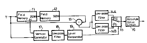
Referring to FIG. 8, a luminance sign Y is
separated from an input video signal by a comb-fllter
(not shown) which uses for example, a line correlation
which is supplied to a field memory 11 which forms a
delay line. The field memory 11 is formed of a so-
called 3-port field memory and has a first output
terminal which has a time delay of 263H and a second
output terminal has a kime delay llH, where H is one
-~ horiæontal line period. The output signal developed
at the first output terminal of the field memory 11 is
supplied to a field memory 12 which forms a delay line
and the time delay of the field memory 12 is selected
to be 262H. Thus, the time delay of the series
circuit of the field memories 11 and 12 is selected to
be one frame (263H + 262H).
The input signal to the field memory 11 and the
output signal from the field memory 12 are supplied to
a subtracter 13, where they are subtracted from each
other to provide a frame difference signal. The frame
difference signal from the subtracter 13 is supplied
to low-pass filters 14A and 14B, one of which is used
to remove a high band noise component and the other to
.
: -
:.
132224~
- 14 -
remove a dot interference component. The low-pass
filter 14A might be a COS filter which has a frequency
response characteristic which is around 3.58 MHz which
corresponds to a frequency of, for example, the dot
interference component. Th~ frequency characteristic
of the low-pass filter 14A is represented by the solid
line a in FIG. 5. On the other hand, the low pass
filter 14B might be a COS2 filter which has a frequency
response characteristic which is around 3.58 MHz which
corresponds to a frequency of, for example, the dot
interference compon~nt. The frequency characteristic
of the low-pass filter 14B is represented by the
broken line ~ in FIG. 5.
The output signals from the low-pass filters 14A
and 14B are supplied to fixed contacts a and b of a
change-over switch 15, respectively. Th~ output
signal from thP change-over switch 15 i~ supplied to
an absolute value circuit 16, where it is converted to
an absolute value. The output signal from the
absolute value circuit 16 is a moving detection
signal.
Referring to FIG. 8, there is shown a vertical
correlator 17 which is supplied th~ input signal to
the field memory 11 and the output signal developed at
the second output terminal of the field memory 11.
The vertical correlator 17 generates an absolute value
of a line difference signal. The output signal from
'
,
,
; ,
~32~2~1
~ 15 -
the vertical correlator 17 is supplied through a low-
pass filter 18 which removes noise components, to a
level comparator 19. The level comparator 19
generates a signal of high level "1" when the line
difference signal supplied thereto is higher than a
predetermined level and a signal of low level "Q" when
it is lower than the predetermined level. In other
words, the level comparator 19 generates a signal of
low level "0" in the vertical correlation portion and
a signal of high level "1" in the vertical non-
correlation portion (vertical edge).
The above-mentioned change-over switch 15 is
controlled by the output signal of the level
comparator 19, and the fixed contact a is engag~d
during the vertical correlation portion and the fixed
contact b during the vertical non-correlation portion.
In this embodiment of the moving detection
circuit thus arranged, the attenuation factor is
switched to the steep low-pass filter 14B during the
vertical non-correlation portion (vertical edge) so
that the dot interference somponent frequency
contained in the vertical edge can he effectively
removed. Further, during the vertical correlation
portion (the portion which is not the vertical edge),
the attenuation factor is switched to the gentle low-
pass filter 14A so that a movement of relatively high
frequency can be detected.
, -:
.
- 12 ~-2 ~ ~ .
A second emb~diment of th~ moving detection
circuit according to the present inven~ion will be
described hereinunder with reference to FIGS. 9 and
10 .
Referring initially to FIG. 9, a video signal
which is applied to an input terminal 1 is supplied to
a Y/C separating circuit 2, in which it is separated
to form a luminance signal Y and a chrominance signal
C. The Y/C separating circuit 2 is formed of a comb-
filter which makes effective use of, for example, a
line correlation.
The luminance signal Y from the Y/C separating
circuit 2 is converted to a digital signal by an A/D
converter 3~, and is then fed to a signal processing
circuit 5Y. The chrominance signal C from the Y/C
separating circuit 2 is supplied to a chroma decoder
4, in which it is decoded to provide red and blue
color difference signals R~Y and B-Y. The red and
~: blue color difference signals R-Y and B-Y from the
chroma decoder 4 are supplied to an A/D converter 3C,
: in which they are converted to digital signals, and
are then fed to a signal processing circuit 5C as
time-division signals R-Y/B-Y.
The signal processing circuits 5Y and 5C perform
signal processing such as interpolating the scanning
line and the liXe. The double-speed luminance signal
and color difference signals from the signal
.
~ 32~
- 17 -
processing circuits 5Y ~nd 5c are converted to analog
signals by D/A conver ers 6Y, 6R and 6B, respectively.
In FIG~ 9 there is shown a clocx generator 7.
When it is supplied with a horizontal synchronizing
signal HD separated from the video signal, the clock
generator 7 generates a clock signal CLKH which is
phase-locked to the horizontal synchronizing signal
HD. The clocX signal CLKH from the clock generator 7
is supplied to a digital processing system and to the
A/D converters 3Y and 3C to the D/A converters 6Y, 6R
and 6B.
The double-speed luminance signal and color
difference signals from the D/A converters 6Y, 6R and
6B are supplied to a matrix circuit 8. ~he double-
speed red, green and blue signals R, G and B from the
matrix circuit 8 are supplied through amplifiers 9R,
9G and 9B to a color CRT 10, where a video signal is
displayed on the screen of the color CRT 10 according
to the non-interlaced scanning system in which the
number of scanning lines is doubled.
FIG. 10 illustrates the arrangement of the signal
processing circuits 5Y and 5C more fully. First the
signal processing circuit 5Y of the luminance signal
sy~tem will be sxplained.
As shown in FIG. 10, the luminance signal Y is
converted to a digital signal by the A/D converter 3Y
(FIG. 9) and is supplied to a field memory 501Y which
:
:~,
1~22~1
- 18 -
forms a delay line. The field memory 501Y is formed
as a so-called 3-port field memory and has a ~irst
output terminal which has a time delay of 263H and a
second output te~ninal which has a time delay time of
262H. The output signal developed at the first output
terminal of the field memory 501Y is supplied to a
field memory 502Y which forms a delay line. The time
delay of the field memory 502Y is selected to be 262H.
Th2 output signal from the field memory 502Y is
supplied to a field memory 503Y which forms a delay
line. The time delay of the field memory 503Y is
selected to be 262H.
The input signal to the field memory 501Y and the
output signal from the field memory 532Y are supplied
to an adder 504Y, where they are added and averaged.
The output signal from the adder 504Y is multiplied by
1 - K (K < 1) by a multiplier 507Y, and it is then fed
to an adder 511Y. The output signals developed at the
first and second output terminals are supplied to an
adder 505Y where they are added and averaged. The
output signal from the adder 505Y is mu]tiplied by K
by a multiplier 508Y, and then fed to the adder 511Y.
The output signal developed at the second output
terminal of the field memory 501Y and the output
signal from the field memory 503Y are supplied to an
adder 506Y, where they are added and averaged. The
output signal from the adder 506Y is multiplied by
.~
2 ~ 1
-- 19 --
1 - K by a multiplier 509Y, and then fed to an adder
S12Y. The output signal at the second output terminal
of the field memory 501Y is multiplied by K by a
multiplier 510Y, and then fed to the adder 512Y.
The value K in the multipliers 507Y through 510Y
is controlled by a moving detection signal which will
be described later, and the value is changed in
response to the amount of movement. By way of
example, K = 0 for the still picture portion and the
maximum valu of K i5 selected to be 1.
The above-mentioned field memories 501Y to 503Y,
adders 504Y to 506Y, 511Y and ~12Y and multipliers
507Y to 510Y constitute a scanning line interpolating
circuit 500Y.
FIG. 11 is a schematic diagxam showing a scanning
line structure from a time - vertical surface
standpoint, wherein an open circle represents a
scanning line of each field. Assuming that in the
scanning line interpolating circuit 500Y, a is the
input signal to the field memory 501Y, c is the output
signal of the first output terminal of the field
memory 501Y, b is the output signal at the second
output terminal thereof, d is the output signal of the
field memory 502Y and e is the output signal from the
field memory 503Y, and signals a to e are plotted in a
positional relationship such as shown in FIG. 11.
~.
.
~3222~
- 20 -
In the scanning line interpolating cixcuit 500Y,
the output signal b at the second output terminal of
the field memory 501Y becomes a main scanning line
signal of the real moving picture and the output
signal ~L~_~ of the adder 506Y becomes a main scanning
line signal of the still picture portion so that the
adder 512Y generates a main scanning line signal Ym in
which the main scanning line signals of the real
moving picture and the signals of the still picture
portion are added with a ratio which corresponds to
the amount of the movement. Also, the output signal
a + d of the adder 504Y becomes the interpolating
scanning line signal of the still picture portion and
the output signal b + c of the adder 505Y becomes the
interpolating scanning line signal of the real moving
picture so that the adder 511Y generates an
inkerpolating scanning line signal Yc in which the
interpolating scanning line signals of the real moving
picture and of the still picture portion are added
with a ratio which corresponds to the amount of
movement. The scanning line to be interpolated is set
at the position shown by a broken line circle in FIG.
11 .
The main scann.ing line signal Ym and the
interpolating scanning line signal Yc from the
scanning line interpolating circuit 500Y are supplied
to a timebase-compressing circuit 521Y. The timebase-
~3222~
- 21 -
compressing circuit 521Y time-compresses each of th~
main scanning line signals Ym and the interpolating
scanning line signals ~c by one half and successively
generates the timebase~compressed signals. In other
words, the timebase-compressing circuit 52lY generates
the double-speed luminance signal.
As shown in FIG. 10, the input signal to the
field memory 501Y and the output siynal from the field
memory 502Y are supplied to a subtracter 531A where
they are subtracted from each other.
The frame difference signal from the subtracter
531A is supplied to low-pass filters 532A1 and 532A2,
each of which is used to remove high band noise
components and dot interference components. The 1QW
pass filters 532A1 and 532A2 are selected to have
filter characteristics which are similar to those of
the low-pass filters 14A and 14B shown in the example
of FIG. 8. The output signals from the low-pass
filters 532A1 and 532A2 are respectively supplied to
fixed contacts a and b of a change-over switch 53SA.
The output signal from the change-over switch s35A is
supplied to an absolute value circuit 533A, where it
is converted to an absolute value, and is then fed to
an adder 534.
The output signals at the second output terminal
of the field memory 501Y and the output signal from
the field memory 503Y are supplied to a subtracter
~5~
~ '~
' ~
' '
~32~
- 22 -
531B where they are subtracted from each other.
The frame difference signal from the subtracter
531B is supplied to low-pass filters 532B1 and 532B2
each of which is used to remove the high band noise
component and the dot interference component. The
filter characteristics of the low-pass filters 532B1
and 532B2 are the same as those of the filters 14A and
14B shown in the example of FIG. 8. The output
signals of the filters 532Bl and 532B2 are respectively
supplied to fixed contacts a and b of a change-over
switch 535B. The output signal from the change-over
switch 535B is supplied to an absolute value circuit
533B where it is converted to an absolute value, and
is then fed to the adder 534.
In FIG. 10, there is shown a vertical correlator
551 which is supplied with the ou put signals
developed at the first and second output terminals of
the field memory 501Y. The vertical correlator 551
generates an absolute value line difference signal.
The output signal from the vertical correlator 551 is
supplied through a low-pass filter 552 which i5 used
to remove a noise component to a level comparator 553.
The level comparator 553 generates a signal of high
level "1" when the line difference signal supplied
~' 25 thereto is higher than a predetermined level and a
- signal of low level 1-0l' when it is lower than the
predete~mined level. In othar words, the level
~,~;,.
.. ,~ .
~32~
23 -
comparator 553 genarates a signal of low leYel "0" in
the vertical correlation portion and a signal of high
level "1" in the vertical non-correlation portion
(vertical edge).
The above-mentioned change-over switches 535A,
535B are controlled by the output signal from the
level comparator 553. In the vertical correlation
portion, the change-over switches 535A and 535B are
each connected to the fixed contact a and in the
vertical non-correlation portion to the fixed contact
b.
The above-mentioned field memories 501Y to 503Y,
the subtracters 531A and 531B, the low-pass filters
532A1, 532A2, 532B1 and 532B2, the absolute value
circuits 533A and 533B, the adder 534, the change over
switches 53~A and 535B, the vertical correlator 551l
the low-pass filter 552 and the level comparator 553
constitute a moving de~ection circuit 530. In this
case, the output signal of the adder 534 increase~ as
the movement increases.
The output signal of the adder 534 is supplisd to
a coefficient generator 541 as the movement detection
signal. The value X of tha above-mentioned
multipliers 507Y through 510Y is gsnerated by the
coefficient generator 541 and varies in response to
the level of the movement detection signal.
The signal processing circuit 5C of the
'
c~
~3222~
- 2~ -
chrominance signal system will be described next.
The signal processing circuit 5C is formed of a
scanninq line interpolating circuik 50GC and a
timebase-compressing circuit 521C. The scanning line
interpolating circuit 500C is formed in a manner
similar to the scanning line interpolating circuit
500Y in the above-mentioned signal processing circuit
5Y. The value of the coefficient of ~he multiplier in
the scanning line interpolating circuit 500C is
generated by the coefficient generator 541.
The scanning line interpolating circuit 500C is
supplied with the time-division signal R-Y/B-Y of red
and blue color difference signals R-Y and B-Y which
are converted to digital signals by the A/D converter
3C (see FIG. 9~, and circuit 500C generates the main
scanning line signal Rm-Ym/Bm-Ym and the interpolating
scanning line signal Rc-Yc/Bc-Yc.
The main scanning line signal Rm-Ym/Bm-Ym and the
interpolating scanning line signal Rc-Yc/Bc-Yc from
the scanning line interpolating circuit 500C are
supplied to the timebase-compressing circuit 521C.
The timebase-compressing circuit 521C time-compresses
each of the main scanning line signal Rm-Ym/Bm-Ym and
the interpolating scanning line signal Rc-Yc/Bc-Yc by
~5 one half and successively generates the timebase-
compressed signals. In this case, the timebase-
compressing circuit 521C separ~tely generates the red
i~3222~
- 25 -
and blue color difference signals. The timebase
compressing circuit 521C generates as a result the
double-speed color difference signals.
In the scanning line interpolating circuit 500Y,
the main scanning line signal b + e and the
interpolating scanning line signal a + d of the
still picture portion are respectively the average
signals in the frame so that the dot interference
components ~chrominance signal components~ contained
in the luminance signal Y cancel out each other.
Also, in the scanning line interpolating circuit 500C,
similar signal processings are carried out, whereby
the cross color components contained in the time-
division signal R-/B-Y cancel out each other. In
other words, the chrominance signal derived from the
Y/C separating circuit 2 (see FIG. 9) is expressed by
a conceptual equation of YH + COSin 2 ~fsc t where ay~
is the luminance signal component and fsc is the color
subcarrier frequency. Thus, when this chrominance
signal is decoded, it is expressed by the following
equation.
Chrominance signal x sin2 fsc 5
= YHsin2~fsc t + C
Thus, the cross color component YH. sin2 fsc t will be
equiphase with the chrominance signal component and is
in a phase-inverted relationship between the frames so
that it is cancelled and removed by the scanning line
: ,
~ . :
~ 3 2 ~
26 -
interpolating circuit 500C
Also, in the scanning line interpolating circuits
500Y and 50QC, the interframe adding processing is
carried out for the still picture portion whereby the
random noise in the time direction is reduced to 1/~2.
Hence, the signal-to-noise (S/N) ratios of th~
luminance signal and the chrominance signal are
increased.
Further, since the moving detection circuit 530
generates the moving detection signal from two frame
difference signals, it is possible to detect the quick
motion between the fields (1/60 second). For example,
when the signals a, b, c and d are represented as
shown in FIGS. 12A, 12B, 12C and 12D, respectively,
the output signals from the ~ubtracters 531A and 531B
respectively become as shown in FIGS. 12E and 12F.
Consequently, the portion P is determined as the still
picture portion by the output signal from the
subtracter 531A so that the movement between the
fields cannot be detected. Thus, with the employment
of the output signal from the subtracter 531B, the
moving detection signal becomes as shown in FIG. 12G
so that the quick motion between the fields can be
- detected.
According to the present embodiment of the moving
detection circuit thus arranged, in the moving
detection circuit 530, the low-pass filters 532~2 and
' .
.'~
, . : . .
22241
532B2 which have steep attenuation factors are used
with respect to the vertical non-correlation portion
: (vertical edge) while the low-pass filters 532A1 and532B1 which have gentle attenuation factor are used
with r~spect to the vertical correlation portion (not
the vertical edge), whereby an action and effect
similar to those of the example shown in FI~. 8 are
achieved.
While in the above-mentioned embodiment the two
low-pass filters are controlled by switches, the
present invention can be modified such that filters
having various characteristics are selectively
switched in response to the degree of vertical
correlation in a similar fashion.
The most specific feature of a third embodiment
of the present invention is that a television signal
has a large correlation in the vertical direction and
:-. movement can be detected even by the field difference
signal in the vertical correlation portion. The third
embodiment of the moving detection circuit according
to the present invention will be described hereinunder
with reference to FIG. 13.
Referring to FIG. 13, the luminance signal Y
which has been separated from the input video signal
by the Y/C separating circuit is supplied to a field
: memory lOl which forms a delay line and the time delay
of the field memory lOl is selected to be 263H. The
.
.
~3222~
- 2~ -
output signal from the field memory 101 is supplied to
a field memory 102 and the time delay of the field
memory 102 is selected to be 262H. Thus, the time
delay of the series circuit of the field memories 101
and 102 is selected to be one frame (263H ~ 262H).
The input signal to the field memory 101 and the
output signal from the field memory 102 are supplied
to a subtracter 103, where they are subtracted from
each other. The frame di~ference signal from the
subtracter 103 is supplied through a low-pass filter
104 to a fixed contact a of a change-over switch 105~
The low-pa~s filter 104 is used to remove a high band
noise component and a dot interference component.
The input signal and the output signal of the
field memory lol are supplied to a subtracter 106 and
are subtracted from each other. The field difference
signal from the subtracter 106 is supplied through a
low-pass filter 107 to a fixed contact b of a change-
over switch 105. The low-pass filter 107 is used to
remove a high hand noise component and a dot
interference component.
The output signal from the change-over switch 105
is converted to an absolute value by an absolute value
. circuit 108. The output signal of the absolute ~alue
circuit 108 is used as a moving detection signal.
In FIG. 13, refer~nce numeral lllA denotes a
vertical correlation detector which is directly
., ~.~
13222~
suppliad with tha input signal of the field memory 101
or via a line memory 112A which forms a delay line.
The vertical correlation detector lllA detects the
existence or nonexistence of the vertical correlation
on the basis of the line difference signal. The
vertical correlation detector lllA generates a signal
of low level "0" in response to, for example, the
vertical correlatlon portion and a siynal of high
level "1" in response to the vertical non-correlation
portion~ A vertical correlation detector lllB is
directly supplied with the output signal of the ~ield
memory 101 or via a line memory 112B which forms a
delay line. The vertical correlation detector lllB
detects the existence or nonexistence of the vertical
correlation on the basis of the line difference
signal. The vertical correlation detector lllB
generates a signal of low level 1l0ll in response to,
~or example, the vertical correlation portion and a
: signal of high level "1" in response to the vertical
non-correlation portion.
The output signals of the vertical correlation
detectors lllA and lllB are calculated by a logic
circuit 113. The output signal from the logic circuit
113 is used to control the above-mentioned change-over
switch 105 so that the position of switch 105 is
changed at a predetermined timing. That is, when the
vertical non-correlation portion is detected by any
~,,~
æ
' .
132~2~1
- 30 -
one of the vertical correlation detectors lllA and
lllB, the change-over switch 105 is connected to the
fixed contact a. The change-over switch 105 is
connected to the fixed contact b for other cases.
According to this embodiment, when the vertical
non-correlation portion is not detected by any one of
the vertical correlation detectors lllA and lllB, or
in the vertical correlation portion, the change-over
switch 105 is connected to the fixed contact b
thereof, whereby the field difference signal, which is
the output signal from the subtracter 106, is
delivered through the low-pass filter 107, the change-
over switch 105 and the absolute value circuit 108 as
the moving detection signal. According to this
embodiment, it is possible to detect quick motion at
the field frequency unit.
FIGSo 14 and 15 ~ach illustrate a scanning line
structure from a time-vertical surface standpoint,
wherein an open circle and a hatched circle represent
white and black main scanning lines, respectively.
Assuming that a is the input signal of the field
; memory 101, b is the output signal thereof, c is theoutput signal of the field memory 102 and d is the
signal advanced from the signal b by one horizontal
; 25 line period in FIG. 13, then these signals a to d are
set in positional relationships shown in FIGS. 14 and
15.
,~
i ~32~2~
- 31 -
Let it be assumed that the output signal b of the
field memory 101 is a signal of the vertical edge as
~hown in FIG. 14. In this case, if the field
difference signal is used as the moving detection
signal, then the moving de~ection signal i5
represented as ¦ a = b ¦~ 0, resulting in the real
moving picture mode. Thus, the signal e on the
interpola~ing scanning line to be interpolated at the
portion shown by a broken line open circle shown in
lo FIG. 14 becomes, for example, ~ (b ~ d), resulting in
line flicker ~eing produced on the line as viewed from
the direction A.
With the above-mentioned circuit arrangement
shown in FIG. 13, when the vertical non-correlation
portion (vertical edge) is detected by the vertical
correlation detector lllB, the change-over switch 105
is connected to the fixed contact a so that the frame
difference signal, which is the output signal from the
subtracter 103, is delivered through the low-pass
filter 104, the change-over switch 105 and the
absolute value circuit 108 as the moving detection
signal. If the frame difference signal is employed as
the moving detection signal, the moving detection
signal is represented as a - c = 0, resulting in the
still picture mode. Thus, the signal e of the
interpolating scanning line to be interpolated at the
portion shown by a broken line open circle in FIG. 14
.' ' , . . ' .
.. ' ' '. ' '
."', ' .
'.
` ~3~2~
- 32 -
becomes, for example, a which avoid the occurrence o~
line flicker.
Let us now consider that the input signal to the
field memory 101 is the signal at the vertical edge as
shown in FIG. 15. In this case, if the field
difference signal is used as the moving detection
signal, the moving det~ction signal i5 represented as
¦ a - b ¦~ 0, resulting in the real moving picture
mode. Thus, the signal e on the interpolating
scanning line to be interpolated at the portion shown
hy a broken line open circle in FIG. 15 becomes, for
exampl~, ~ (b ~ d) so that the line flicker occurs on
the line as viewed from the direction A.
Wi~h the above-mentioned circuit arrangement,
when the vertical non-correlation port.ion (vertical
edge) is detected by the vertical correlation detector
lllA, the change-over switch 105 is connected to the
fixed contact a so that the frame difference signal,
which is the output signal from the subtracter 103, is
delivered through the low-pass filter 104, the change-
over switch 105 and the absolute value circuit 108 as
the moving detection signal. If the frame difference
signal is employed as the moving detection signal,
then the moving detection signal is represented as
¦ a - c ¦- , resulting in the still picture mode.
Thus, the signal e on the interpolating scanning line
to be interpolated at the portion shown by a broken
~ P~
~ ~322241
- 33 -
line open circle in FIG. 15 becomes, as for example,
a, thus avoiding line flicker.
FIG. 16 illustrates a fourth embodiment of the
moving detection circuit 530 according to the present
in~ention.
As shown in FIG. 16, the field memories 510Y to
503Y of the scanning line interpolating circuit 500Y
in the example shown in FIG. 10 are also used as the
field memories 501Y to 503Y in FIG. 16.
Referring to FIG. 16, the input signal to the
field memory 5QlY and the output signal from the field
memory 502Y are supplied to the subtracter 531A, where
they are subtracted from each other.
The frame difference signal from the subtracter
531A is supplied to low-pass filters 532A1 and 532A2,
which are used to remove a high band noise component
and a dot interference component. The low-pass filter
532A1 might be a COS filter which has a low frequency
response of around 3.58 MHz which corresponds to a
frequency of, for example, a dot interference
component. The frequency characteristic of the low-
pass filter 532A1 is represented by the solid line a in
FIG. 5. The low-pass filter 532A2 might be a COS2
filter whose response characteristic may be low around
3~58 MHz which corresponds to the frequency of, for
example, a dot interference component. The frequency
characteristic of the low-pass filter 532A2 is
, :
~2~
- 34 -
represented by the broken line b in FIG. 5.
The output signals of the low-pass filters 532Al
and 532A2 are supplied to fixed contacts a and b of a
change-over switch 535A, respectivelyO The output
signal from the change-over switch 535A is supplied to
an absolute value circuit 533A, where it i~ converted
to an absolute value and is then fed to an adder 534.
The output signals at the second output terminal
of the field memory 501Y and of the field m~mory 503Y
are suppl.ied to the subtracter 531B and are subtracted
from each other.
A frame difference signal from the subtractar
531B is supplied to low-pass filter 532B1 and 532B2
which are used to remove a high band noise component
and a dot interference component. The characteristics
of the low~pass filters 532B1 and 532~32 are selected to
be similar to those of the low-pass filters 532A1 and
532A2, respectively. Ths output signals of the filters
532B1 and 532B2 are supplied to fixed contacts a and b
of a chan~e-over switch 535B, respectively. The
output signal from the change-over switch 535B is
converted to an absolute value by an absolute value
circuit 533B and is then fed to the adder 534.
The output signal of adder 534 is supplied to an
adder 536 as a low band moving detection signal.
The output signals of the subtracters 531A and
53lB are respectively supplied through band-pass
:
~3~22~1
~ ~5 -
filters 537A and 537B to a subtracter 538. The center
freguencies of the ~and-pass filters 537A and 537B are
each selected to be 3.58 MHz which corresponds ko the
frequency of the chrominance signal component~ The
output signal of the subtracter 538 is converted to an
absolutQ value by an absolute value circuit 539, and
is then supplied through a switching circuit 554 to
the adder 536 as a high band moving detection signal.
The output signal of the adder 536 is the moving
detection signal.
In FIG. 16, reference num~ral 551 designates a
vertical correlator. The vertical correlator 551 is
supplied with the output signals of the first and
second output terminals of the field memory 501Y. The
vertical correlator 551 generates an absolute value
signal of the line difference signalO The output
signal of the vertical correlator 551 is supplied
through a low-pass filker 552 to a level comparator
553. The low-pass filter 552 is used to remove noise
components. The leval comparator 5~3 generates a
signal of high level "1" when the line difference
signal supplied thereto is higher than a predetermined
: level and a signal of low level lOIl when it is lower
than the predetermined level. In other words, the
level comparator 553 generates a signal of low level
"0" for the vertical correlation portion and a signal
of high level "1" for the vertical non-correlation
,~, ,~,,
1~222~
- 36 -
portion ~vertical edge).
The change-over switches 535A and 535B are
controlled so as to change position by the output
signal from the level comparator 553 so that the
moveable contacts are connected to the fixed contact a
for the vertical correlation portion and to the fixed
contact b for the vertical non-correlation portion.
The above-mentioned switching circuit 554 is
controlled by the output signal of the level
comparator 553 so that it supplies its input signal
for the vertical correlation portion and supplies a
æero output signal from the vertical non-correlation
portion.
The above-mentioned moving detection circuit 530
obtains a low band moving detection signal by adding
the two frame difference signals so that it is
possible to detect a quick motion between the fields
(1/60 second). For example, when the signals a, b, d
and e are, respectively as represented in FIGS. 17A,
17B, 17C and 17D, the output signals of the
subtracters 531A and 531B are represented as shown in
FIGS. 17E and 17F, respectively. Consequently, the
portion P is determined as the still picture portion
from only the output signal of the subtracter 531A,
which makes it impossible to detect motion between the
fields. Thus, with the employment of the output
signal from the subtracter 531B, the moving detection
.
~ ~222~1
- 37 -
signal is as shown in FIG. 17G, where quick mov~ments
between the fields can be detected.
Further, at the vertical non-correlation portion
(vertical edge), the low-pass filters 532A2 and 532B2
each have a steep attenuation characteristic, while at
the vertical correlation portion (portion which is not
the vertical edgej, the low-pass filters 532Al and
532Bl are utilized, so that the dot interference
component can be effectively removed and also,
movement of relatively high frequency can be
sufficiently detected.
The band-pass filters 537A and 537B generate the
high band components of the frame difference signals,
and the subtracter 538 generates a difference signal
;~ 15 of the frame difference signals. In this case, as
shown in FIG. 18, the dot interference components
(chrominance signal components) have a phase-inverted
relationship between the frames and between the lines
so that the high band components of the frame
difference signals derived from the band-pass filters
537A and 537B, respectively, contain the dot
interference components. In case of a still picture,
these dot interference components become equal in
amplitude and phase as shown in FIGSo l9A and l9B, and
the difference signal from the subtracter 538 becomes
zero a5 shown in FIG. l9C.
Thus, the detection error due to the dot
:''
~3~2~
- 38 -
interference component can be avoided and the high
band moving detection signal can be satisfa~torily
obtained.
Further, in the vertical non-correlation portion,
the chrominance signal components are not inverted
between the lines as shown in FIG. 20, and the dot
interference components contained in the high band
components of the frame difference signals fxom the
band-pass filters 537A and 537B do not become equal in
amplitude and phase as shown in FIGS. 21A and 21B even
for a still picture. The difference signal from the
subtracter 538 is as a result represented in FIG. 21C
and forms a detection error signal. In the example
shown in FIG. 16, in the vertical non-correlation
portion, the switching circuit 554 produces a zero
output signal~ and the difference signal is not used
as the moving detection signal. It is ther~ore
possible to prevent detection errors from being caused
because of the dot interference component~
In FIGS. 18 and 20, the open circle represents
the scanning line of each field, the broken line
circle the position of the scanning line which is to
be interpolated, and the symbols ~ and ~, the phases
~ of the dot interference components, respectively..~ 25 FIG. 17 shows the pattern by which the moving
detection signal cannot be obtained in the moving
detection operation of the low band, and the moving
. ~'' ' .
~322~1
- 39 -
detection signal can be obtained in the moving
detection operation of the hiyh band. FIGS. 17A, 17B,
17C and 17D, respectively, illustrate the input signal
to the field memory 510Y and the output signals of the
field memories 501Y, 502Y and 503Y shown in FIG. 16.
For that condition, the output signals of the
subtracters 531A and 531B are as shown in FIGS. 17E
and 17F, respectively.
The output signals of the ubtracters 531A and
531B are not delivered from the low-pass filters 532A1,
532A2, 532B1 and 532B2, and the low band moving
detection signal from the adder 534 becomes zero as
shown in FIG. 17H. The output sign~ls of the
subtracters 531A and 531B are delivered from the band- :
pass filters 537A and 537B, and the high band moving
detection signal from the subtracter 538 i5 as shown
in FIG. 17G. Also, the frequencies of the output
signals ~shown in FIGS9 17E and 17F) from the
subtracters 531A and 531B are frequencies outside the
pass bands of the low-pass filters 532A1, 532Az, 532
and 532B2.
: In the above-mentioned embodiments, the high band
moving detection signal is obtained from the luminance
signal which has been separated from the video signal
by the Y/C separating circuit. If the input signal,
for example, is a composite video signal, then it is
possible to detect the movement of the chrominance
'
~ 3~22~
~ 40 -
signal C as well as the movement of the luminance
signal Y in the high band.
While in the above-mentioned embodiments the
band-pass filters 53-lA and 537B are employed, the
band pass filters 537A and 537B may be replaced with
high-pass f ilters. The filters used need only be
filters which can block a signal of a low frequency
band.
According to the present invention, as set out
above, since the filters for passing the frame
difference signals are switched by the output signals
from the vertical correlation detectors, the dot
interference component (chrominance signal component)
at the vertical edge can be effectively removed and
movement of relatively high frequency can be
adequately detected.
Further, according to the present invention,
since the field difference signal is used as the
moving detection signal for the vertical correlation
portion, it is possible to detect quick motion of the
field frequency unit. In addition, since the frame
difference signal is used as the moving detection
signal for the vertical non-correlation portion,
detection errors can be prevented and also line
flicker or the like can be prevented.
Furthermore, according to the present invention,
since the first and second frame difference signals
~.
13~2~
- 41 -
which each have a time difference of one field period
are obtained from the video signal and the difference
signals of high band components are used as the high
band moving detection signals, the high band moving
detection signal can be obtained without causing
detection errors due to the chrominance signal
components (dot interference components~. Thus, as
compared with moving detection using only the low
frequency band, it is possible to substantially
increase the detection capability of the moving
detection circuit. Further, since the switching means
is controlled for the vertical non-correlation portion
so that the difference signal of the high band
component is not used as the moving detection signal,
it is possible to avoid the occurrence of detection
; errors.
It should be understood that the above
description i5 presented by way of example for the
preferred embodim~nts of the invention and it will be
apparent that many modifications and variations
thereof could be effected by one skilled in the art
without departing from the spirit and the scope of the
. novel concepts of the invention so that the scop~ of
the invention should be determined only by the
appended claims.
~.