Note: Descriptions are shown in the official language in which they were submitted.
~3~2398
1 -- .
The present invention relates to an electromag~etic
wave shielding transparent body having excellent :.
electromagnetic wave shielding properties, wh.ich is
suitable for application to window~ or doors.
In recent years, noises due to electromagnetic waves
have been a serious problem for buildings or various
other structures~ In order to overcome ~uch a pro~lem of
noises due ~o elec~romagnetic waves, i~ has been desixed
to develop a techni~ue to preve~t external
elec~romagnetic wave~ from enteri~g in~o buildings ~o
that electronic mac~ines or equipmen~s in ~he buildings
will not be affected by the noises of the external
~lectromagnetic ~aves and a technique to prevent leakage
of electromagnetic waves from the interior of the
buildings to the exterior so that the internal
electromagnetic waves ~ill not adversely affect other
buildings. Such tech~iques to pr~vent the leakage of
electromagne~ic waves and to prevent the entrance of
electromagnetic waves are required particularly for
.
~2~398
- 2 --
intelligent buildings wherein optical fiber cables,
coaxial cables or information network systems for e.g.
radio communications, are ramified, for computer centers
or ~or buildings, offices or hospitals wherein high
precision electronic equipments are used, with a view to
preventing the generation o~ noises, erroneous operations
or leakage of information, ox with a view to the
prevention of tapping of information. The necessity for
such techniques is expected to increase even more in the
future. Further, a~ a site where the electromagnetic
environment is poor, e.g. at a site close to an electric
train or to a high-voltage transmission line, an
electromagnetically shielded building i~ required to
preven~ the ~ntrance o~ the electromagnetic waves.
When such buildings, various other structure~ or
offices designed to prevent the entrance and leakage of
electromagnetic waves, are to be constructed, it is usual
that openings such as windows and doorways are located at
sites where electromagnetic s~lielding effects are most
r~quired. ~eretofore, however, the materials ~or
openings such as windows or doorways, particularly the
materials for windows and openings where transparency is
required, such as glass, have had no electromagnetic wave
shielding properties, and it was therefore impossible to
shield electromagnetic waves at such openings.
Heretofore, buildings having a high level of
electromagnetic wave shielding properties were therefore
.
~2~3~3
windowlessl whereby no sunlight entered, and did not
provide a good working environmentO When an
electro~agnetically ~hielded space is required in a u~ual
buildin~, it used to be required to construct a
windowless eleetromagnetic wave shielding room~ In such
a case, the above-men~ioned drawbacks exist. Under these
circumstances, it has been desired to develop a
transparen~ materiai such as glass w~ich has a high
electroma~netic wave shielding property and a sufficient
t~ansmit~ance of lights in the v;sible ~ight range of
sunlight.
~ eretofore~ w;ndow glass having a high level of an
electromagnetic shielding property and transmittance of
light~ in the vi~ible light range of sunlight, u~ed to be
such that a woven cloth made of fine filaments having a
high level of an electromagnetic ~hielding property, such
a~ a mesh cloth, was sandwiched ~y a pair o glass
sheets, or such that a metal layer having a substantial
thickness was bonded to a glass sheet. The former was
u~satis~actory with respect to the electromagnetic
shielding pr~perty and had a difficulty in the
transmittance o~ lights in the visible light range of
sunlight. The latter had a drawback ~hat ;t had a
serious problem in the transmittance of lights in the
visible light range of sunlight~
The present invention provides a txansparent material
such as a glass having a
.....
:. X
,
- ~. ' ' ., ~'~
-
~: .,
~223~
-- 4 --
high electromagnetic shielding property and sufficient
transmittance of light~ in the visible light range of
sunlight and being free from the above-mentioned
drawbacks, particularly a transparent body suitable for
use at openings such as windows or doorways of buildings,
structures or rooms for shielding electromagnetic waves.
The present invention provides an electromagnetic
wave shielding transparent body comprising one or more
transparent sheets, a transparent conductive layer formed
as a fir3t electric conductor on at least one of said
transparent sheets, and a second electric conductor
separated from ~aid transparent conductive layer.
Now, the present invention will be described in
~ detail wikh reference to the preEerred embodiments.
In the accompanying drawings:
Figures 1 to 5 are cross sectional views of various
embodiments of the electromagnetic wave shielding
transparent body of the present invention.
Figure 6 is a cross sectional view of a glass sheet
in which a metal wire is sealed in the form of a lattice,
as an embodiment of a transparent sheet having a
conductive lattice pattern formed as ~he second electric
conductor of the present invention.
Figures 7 to 10 are plan views of electromagnetic
wave shielding transparent bodies of the present
invention having various conductive lattice patterns
formed as the second electric conductor of,the present
- .... .
.
:' ~ ', . -:. ` .
. : .. :;
::: : ....
~ 32~
invention.
Figure 11 is a partially omitted diagrammatical
illustration of an electromagnetic wave shielding
transparent body of the present invention having a highly
conductive lattice provided as the second electric
conductor of the present invention in an inner space of a
multi-layered transparent assembly.
Figures 12 to 16 are partially omitted cross
sectional views of various electromagnetic wave shielding
transparent bodies of the present inven~ion having a
highly conductive lattice provided as the second electric
conductor of the present invention.
Figures 17 and 18 are partially omitted cross
sectional views illustrating difEerent embodiments oE the
earth connection of electromagnetic wave shielding
transprarent bodies of the present invention.
Figures l9(a) and l9(b) are cross sectional views of
electroma~netic wave shielding transparent bodies of the
present invention having filaments provided on the
respective transparent conductive layers.
Figures 20(a) and 20(b) are plan views of
electromagnetic wave shielding transparent bodies of the
present invention having filaments provided on a
transparent conductive layer as the first or second
conductor.
Figures 21(a) to 21(f) are cross sectional views o~
transparent sheets having a color or reflectivity-
.
.: ,. .. . .
.: . :. . ...
,, , .. : . . . ..
~32239~
-- 6
adjustiny layer formed on or under the first or second
conductor.
Referring to the drawings, various embodiments of the
present invention will be described.
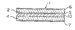
Figures 1 to 5 are cross sectional views of various
embodiments of the electromagnetic wave shielding
transparent body of the present invention. In these
Figures, reference numeral 1 indicates an electromagnetic
wave shielding transparent body~ numerals 2 and 4
indicate transparent sheets, numerals 5 and 6 indicatetransparent conductive layers as the first electric
conductor, numerals 7 and 8 indicate the second electric
conductors, numeral 10 indicates an interlayer, numeral
11 indicates a spacer for a multi-~lazed assembly, and
numeral 12 indicates an inner space.
In the present invention, the transparent sheets may
be transparent, translucent, colored transparent or
colored translucent glass sheets, or various plastic
sheets or films. Among them, glass sheets are preferred
from the viewpoint of optical properties and durability.
Otherwise, such a transparent sheet may be the one
obtained by laminating one or more transparent sheets by
means of an interlayer or an adhesive.
The transparent body of the present invention may be
composed of a single transparent sheet 2 as shown in
Figure 1, or may be of a laminate type as shown in Figure
,~ 2 wherein two transparent sheets 2 and 4 are bonded by an
. . . :., . . ~
~ 32~
interlayer 10. Further, it may be of a double-layered
type as shown in Figure 3 or 4 wherein two transparent
sheets 2 and 4 are spaced with a predetermined distance
from each other by a spacer 11 so as to Eorm an inner
space 12, or of a double-sheet type as shown in Figure 12
wherein two transparent sheets 22 and 23 are spaced with
a predetermined distance from each other by a frame 29 so
as to form an inner space 24. Otherwise, the transparent
body of the present invention may be of a laminate type
wherein three or more transparent sheets are bonded by
interlayers, or of a multi-layered type wherein three or
more transparent sheets are spaced by spacers, or of a
multiple-sheet type wherein three or more transparent
sheets are spaced from one another by a frame. In this
specification, a "multi-glazed" assembly will be used as
the word that includes both multi-layered type and multi-
sheet type assembly.
The electromagnetic wave shielding transparent body
of the present invention comprises a transparent
conductive layer formed as a first electric conductor on
at least one of the above-mentioned transparent sheets,
and a second electric conductor separated from the
transparent conductive layer.
In the present invention, the transparent conductive
layer as the first electric conductor formed on a
transparent sheet includes, for example, not only a
transparent tin oxide conductive layer (a eonductive
. . , : .
. . , I . ;
132239~
layer of tin oxide doped with antimony or fluorine) and a
transparent indium oxide conductive layer (a condutive
layer of indium oxide doped with tin3 but also a single
layered thin film type transparent layer of a metal or
alloy of e.g. Cr, Ti, Ag, Au, Al, Cu or Ni, and a multi-
layered thin film type layer having such a metal or alloy
layer sandwiched between thin dielectric films of e.g.
ZnO~ SnO2, In2O3~ TiO2, Bi2o3~ Ta2O5~ WO3 or
example, a three-layered type such as TiO2/Ag/TiO2,
ZnO/Ag/ZnO, or SnO2/Ag/SnO2, and a ~ive layered type such
as TiO2/Ag/TiO2/Ag/TiO2, or ZnO/Ag/ZnO/Ag/ZnO, as well as
other layers of appropriate constructions. Each of these
transparent conductive layers is made of a film having
high heat ray reflectivity. I~ necessary, however, it i5
possible to employ a ilm having relatively low heat ray
reflectivity. When the transparent conductive layer is
made of a film having high heat ray reflectivity, it hais
a function to reduce the air conditioning load, and as
~uch it can be used as a window material having good heat
insulating properties.
The transparent conductive layer having the above
described construction can be formed by an appropriate
layer-Corming method such as a vacuum vapor deposition
method, a sputtering method, a CVD method, a spray
method, a CLD method or a printing method. In such a
case, the transparent conductive layer is preferably
formed directly on a transparent sheet. ~owever, it is,
,
: . , . . , .. , , .. . . -
. . - . , .
; . . -
.. ..
`` ~ 3 ~ g
possible to employ as the transparent conductive layer a
transparent conductive plastic film formed by laminating
a transparent conductive layer on a plastic film such as
a polyester film and to laminate such a transparent
conductive plastic film on a transparent sheet.
The transparent conductive layer to be used in the
present invention, preferably has a resistance of at most
20 Q/O to obtain a high level of electromagnetic wave
shielding effects. Most preferably, the resistance is at
mo5t lO n/o so that the conductive layer is capable o
effectively shielding electromagnetic waves within a wide
frequency range of at least 40 MHz. The thickness of the
transparent conductive layer is suitably selected so that
the desired resistance and visible light transmittance as
mentioned above will be obtained, or a desired color will
be obtained.
Such a transparent conductive layer may be divided
into two or more films~ so that it may be composed of a
plurality of transparent conductive films. In such a
case, the distance between the respective transparent
conductive films i9 preerably at most l cm to prevent
leakage of electromagnetic waves. When a plurality of
transparent conductive films are formed on one
transparent sheet, the overall electric resistance of the
plurality of transparent conductive films formed on the
transparent ~heet can be reduced by connecting them
electrically in parallel, whereby the electromagnetic
.
~ . :
"
~2~
-- 10 --
wave shielding performance can be improved.
Such a transparent conductive layer may be formed on
the exposed surface of the transparent sheet as shown in
Figure 1, or in the case of a laminate type, it may be
formed on the laminated surface of the transparent sheet
as shown in Figure 2. In the case of the double-glazed
type, it may be formed on the inner space side o~ the
transparent sheet(s) as shown in Figures 3 and 4. By
forming the transparent conductive layer on the laminated
surface or on the inner space side surface as mentioned
above, it is possible to avoid exposure of the
transparent conductive layer and to protect the
transparent conductive layer, such being advantageous in
the case of a transparent conductive layer having poor
durability. It is of course possible to form the
transparent conductive layer on the exposed surface even
in the case of a laminate type, double- or multi-glazed
type transparent sheet.
The transparent conductive layer as the first
electric conductor may be formed on one side of a
transparent sheet. If necessary, however, it may be
~ormed on two or more surfaces. In each of the
embodiments shown in Figures 1, 2 and 3, a transparent
conductive layer 5 is formed on one side of a transparent
sheet 2. In the embodiment shown in Figure 5,
transparent conductive layers 5 and 6 are formed on both
sides of a transparent sheet 2. Figure 4 shows an
.. ~ .. . . ..
3 ~ ~
~ 11
embodiment wherein transparent conductive layers 5 and 6
are formed on one side of the respective transparent
sheets 2 and 4 of a double-layered assembly comprising
two transparent sheets.
In the present invention, the second electric
conductor provided for the purpose of complementing the
electromagnetic wave shielding property of the first
electric conductor, may be a transparent conductive layer
or a conductive lattice pattern, or it may be a lattice
made at least partially of an electrically highly
conductive material. The transparent conductive layer or
the conductive lattice pattern as the second conductor is
preferably formed on at least one of 2n surfaces o~ one
or plurality (n) kransparent sheets constituting the
transparent body of the present invention other than the
surface(s) on which the above-mentioned transparent
conductive layer as the first conductor is formed.
Namely, it is preferred that the transparent conductive
layer as the fir t conductor is formed on one of 2n
surfaces of the transparent sheets, while the second
electric conductor is formed on at least one of the rest
of the ~n surfaces. In Figures 1 to 5, such second
electric conductors are shown by reference numerals 7 and
8. The lattice made at least partly of a highly
conductive material may be provided as the second
electric conductor in an inner space formed between
transparent sheets disposed to face one another with a
:
-
, . . ~ , .......... . .. - ................ . .
;: .. : . , . . :
- 12 -
space Such a structure is illustrated in Figures ll to
16.
As the conductive lattice pattern formed on a
transparent sheet constituting the -transparent body of
the present invention, a lattice pattern formed of a
highly conductive material is employed so as to
efficiently shield electromagnetic wavesO Such a
conductive lattice pattern may be the one formed by
printing a conductive paste comprising a metal powder
such as Ag, Al, Au or Cu and a binder, in a predetermined
lattice pattern, followed by curing or baking, or the one
formed by bonding an aluminum or nicltel foil in a
predetermined lattice pattern, or the one formed by
bonding or sandwiching a plastic film on which or on an
intermediate layer of which a lattice pattern made of a
conductive metal is formed. As a transparent sheet
having such a conductive lattice pattern formed therein,
it is possible to use a glass sheet 3 in which a metal
wire 9 is sealed in the form of a lattice pattern as
shown in Figure 6, or a plastic sheet having a metal wire
net sealed therein. It is also possi~le to employ a
transparent laminate wherein a metal wire is sandwiched
in a lattice pattern between a pair of transparent
sheets. It is also possible to prepare a lattice from an
electrically highly conductive metal or alloy (such as
Al, Cu, stainless steel or brass), or from other
conductive material, or to prepare a lattice from a
,, .
~ .
~ 23g8
- 13 -
plastic material, and then form a coating layer of an
electrically highly conductive metal or alloy, or other
conductive material, on its surface, or to prepare a
lattice from an electrically highly conductive metal or
alloy, or other conductive material, and form a coating
layer or insulating layer on its surface, and to paste,
bond or otherwise fix such an lattice to a transparent
sheet to form a lattice pattern. A lattice pattern
described above may be formed on one surface of a
transparent sheet. If necessary, it may be formed on two
or more surfaces or inside of a transparent sheet.
There is no particular restriction as to the shape in
the front view o each unit of the conductive lattice
pattern. ~ polygonal pattern ~uch as a triangular,
rectangular, pentagonal or hexagonal pattern, or a
pattern of any other optional shape, may be employed.
The length (inner size) of the longer diagonal line of
each lattice unit is determined talcing into consideration
the desired light transmittance, electromagnetic wave
shielding properties, design, etc. U~ually, it is
preferable the length of the diagonal line is from 1 to
30 cm. If it exceeds 30 cm, the electromagnetic wave
shielding properties in a low frequency region tend to
decrease, such being undesirable. On the other hand, i~
it is shorter than l cm, the lattice pattern tends to be
dense, such being undesirable from the viewpoint of see-
through and light transmitting properties.
,
- 14 -
By using an electrically highly conductive lattice
pattern having the above described structure and
dimensions, electromagnetic waves can effectively be
shielded by repetition of reflection of electromagnetic
waves at the respective lattices. Elecl:romagnetic waves
in a low frequency range such as electromagnetic waves of
frequency of not more than 400 MHz can particularly
effectively be shielded.
In the embodiments shown in Figures 7 and 9, a gLass
sheet was used as a transparent sheet, and a silver paste
was printed on the surface of thls glass plate in a
lattice pattern with the shape of each lattice unit being
square, followed by baking to form a conductive lattice
pattern, whereby the length o~ the diagonal line of the
lS rectangular lattice was adjusted to 10 cm, and the
thickness of the lattice pattern was adjusted to 20 ~m,
and the width of the line was adjusted to 1 mm, so that
electromagnetic waves of not higher than 400 MHz can
effectively be shielded.
In the embodiment of Figure 8, a glass sheet was used
as the transparent sheet, and a silver paste was printed
on this glass sheet in a lattice pattern wherein the
shape of the lattice unit was rectangular, followed by
baking to form an conductive lattice patternl whereby the
diagonal line of the rectangular lattice was adjus-ted to
20 cm, the thickness of the lattice pattern was adjusted
to 20 ~m and the width of the line was adjusted to 1 mm,
: - - - ~ .;,:. ,
.! ' ' ' ~
3 ~ ~
- 15 ~
so that electromagnetic waves or not more than 300 MHz
can effectively be shielded.
In the embodiment of Figure 10, a glass sheet was
used as the transparent sheet, and a silver paste was
printed on this glass sheet in a lattice pattern wherein
the shape of the lattice unit was triangular, followed by
baking to form an conductive lattice pattern, whereby the
length of the height of the triangular lattice was
adjusted to 10 cm, the thickness of the lattice pattern
was adjusted to 20 ~um and the width o~ the line was
adjusted to 1 mm, so that electromagnetic waves of not
more than 400 MHz can effectively be shielded.
Figure 11 is a partially omitted diagrammatical
illustration of an electromagnetic wave shielding
transparent body of the present inventionr wherein a
highly conductive lattice as the second electric
conductor of the present invention is provided in an
inner space of a double-glazed transparent assembly. In
this Figure, reference numeral 21 indicates a double-
layered transparent body, numerals 22 and 23 indicatetransparent sheets, numeral 24 indicates an inner space,
numeral 25 indicates a transparent conducti.ve layer, and
numeral 26 indicates an electrically highly conductive
lattice. The double-glazed transparent body 21 is
prepared by disposing a pair of transparent sheets 22 and
23 in parallel to each other with a predetermined space
by a drying agent-containing spacer 27 disposed along the
,' ` ' ' '
" .~ ', ' ' ' '
22398
.
- 16 -
periphery of the transparent sheets and sealing them with
sealant 28 along the peripheral portion to form an inner
space 24 between the two transparent sheets 22 and 23.
As the lattice to be provided in the inner space of
the double-glazed transparent body, as the second
electric conductor of the present invention, an
electrically high conductive latti~e is employed in order
to shield electromagneic waves. This electrically highly
conductive lattice may be the one wherein the lattice is
made of an electrically highly conductive metal or alloy
(such as Al, Cu, stainless steel or brass), or other
conductive material, or the one wherein the lattice is
made of a pla.stic or insulating material and a co~ting
layer of an electrically high conductive metal or alloy,
or other conductive material, is formed on its surface,
or the one in which a lattice is made of an electrically
high conductive metal or alloy, or other conductive
material, and a coating layer or an insulating layer is
provided on its surface. There is no particular
restriction as to the shape in the front view of each
` lattice unit of this lattice. The shape may be
triangular, rectangular, pentagonal, hexagonal or any
other optional shape. The length (the inner size) of the
longer diagonal line of each lattice unit is determined
taking into consideration the desired light
transmittance, electromagnetic wave shielding properties,
design, etc. The length of the diagonal line is usually
..
,~
.~
~22~
- 17 -
from 1 to 30 cm. If it exceeds 30 cm, the
electromagnetic wave shielding properties in a low
frequency region tend to be low, such being undesirable.
On the other hand, if it is shorter than 1 cm, the
lattice pattern tends to be dense, such being undesirable
from the viewpoint of see-through and light transmitting
properties.
By using an electrically highly conductive lattice
having the above described structure and dimensions,
electromagnetic waves can effectively be shielded by
repetition of reflectance of electromagnetic waves at the
respective lattice surfaces. Electromagnetic waves in a
low frequency range, such as electromagnetic waves of
frequency of not more than 400 M~z can particularly
e~fectively be shielded.
Figure 11 illustrates an embodiment wherein an
aluminum metal lattice is used wherein the shape of each
lattice unit is square, whereby the length o~ the
diagonal line is adjusted to from 5 to 15 cm so that
electromagnetic waves of not more than 400 MHz can be
shielded.
In the electromagnetic wave shielding transparent
body of the present invention, the transparent conductive
layer as the first electric conductor, and the second
electric conductor can be in a conductive state.
However, in the case where the second electric conductor
is a conductive lattice pattern or an electrically highly
'' ~
~ ~ ,
.
~32~39~
- 18 -
conductive lattice, it is preferred that the transparent
conductive layer and the conductive lattice pattern or
lattice are in a non-conductive state, so that the
transparent conductive layer is capable of effectively
shielding electromagnetic waves in a high frequency
region (e.g. from 100 to 1,000 M~z), while the lattice
pattern or lattice is capable of effectively shielding
electromagnetic waves in a low frequency region ~e.g. not
more than 400 MMz).
When the second electric conductor is a conductive
lattice pattern, the transparent conductive layer and the
conductive lattice pattern may be formed on different
surfaces of a transparent sheet as mentioned above so
that they are in a non-conductive state to each other.
Otherwise, an electric insulating layer may be provided
between the transparent conductive layer and the
electrically highly conductive lattice at least at the
portion where the two are otherwise in contact with each
other, so that they are in a non-conductive state to each
other.
In a particularly preferred embodiment, a transparent
conductive layer and a conductive lattice pattern are
separately provided on different surfaces of a
transparent body. In this manner r a high electromagnetic
~ave shielding effect can be obtained within a wide
frequency ranye due to the synergistic effects of the
electromagnetic wave shielding properties of the
. . . .. :. . :
~. ~ . , ., . ~,. . .
~, .,; , ,, :,
; ,,; i.. . . . .. .
.. . :~: . .
. . , .:
` ~3223~8
-- 19 --
transparent conductive layer and the conductive lattice
pattern. When the second electric conductor is an
electrically highly conductive lattice, it is preferred
that the transparent conductive layer and the
electrically highly conductive lattice are made to be in
a non-conductive state at least at the central portion of
the transparent sheet on which the tran~parent conductive
layer is formed. In this case, the transparent
conductive layer and the electrically highly conductive
lattice may be in a conductive state along the periphery
of the transparent sheet. In order to make the
~ransparent conductive layer and the electrically highly
conductive lattice to be in a non conductive state, an
electric insulating layer 30 may be ~ormed at the portion
where the two are otherwise in contact with each other,
as shown in Figure 12, or the two may be disposed with a
space so that they are in a non-conductive state.
- Otherwise, the two may be made to be non-conductive by
selecting the sur~ace on which the transparent conductive
layer is formed so that such a surface is not in contact
with the electrically highly conductive lattice.
At least one of the transparent conductive layer as
; the first electric conductor and the electrically
conductive lattice pattern or lattice as the second
electric conductor may be provided with a terminal for
earthing so that the electromagnetic waves thereby caught
are earthed, whereby the electroma~netic wave shielding
,. , . -~
~32239~
- 20 -
effect is obtained. When the transparent conductive
layer and the lattice patten are in a non-conductive
state, a terminal for earthlng is provided to each of
them. When they are in a conductive state r the earthing
terminal may be provided to one of them or each of them.
In the transparent conductive layer and/or ~he lattice
pattern, a conductive paste containing a conductive metal
powder such as Ag or Al is printed along an appropriate
peripheral portion of the transparent conductive layer in
a predetermined pattern, followed by baking or curing to
form a busbar, or an aluminum foil or a copper foil in a
predetermined pattern is bonded to form a busbar, and an
earthing terminal is p~ovided at an appropriate position
of such a bu~bar. To this earthing terminal, a terminal
block may be attached to facilitate the connection with
an earthing line, as the case requires. Such an earthing
terminal may be provided at one position or at a
plurality of positions.
Pigure 17 illustrates an embodiment in which an
electromagnetic wave shielding transparent body 21 of the
present invention comprises transparent sheets 2 and 4
dispoaed with a predetermined space in parallel to each
other by a spacer 27 to form an inner space 12 and sealed
along their periphery with a sealant 28 and first and
second electric conductors 5 and 5 formed on the inner
space sides o~ the transparent sheets 2 and 4~ wherein
aluminum tapes 40 and 42 are provided to contact the
~3~23~8
- 21 ~
electric conductors S and 6, respectively, and extend to
the exterior of the transparent body, so that they may be
earthed.
The transparent conductive layer ancl/or the lattice
pattern may not necessarily be provided with an earthing
terminal. For example, ~hen the transparent sheet is
attached to a window frame, predetermined portions of the
transparent conductive layer and/or the lattice pattern
are exposed, and a conductive sealant is provided along
the exposed portions of the transparent conductive layer
and/or the lattice pattern, so t~at the conductive
sealant îs utilized for the condution with the window
frame.
Figure 18 illustrates an embodiment wherein the
electromagnetic wave shielding transparent body 1 of the
present invention comprises a transparent sheet 2 and the
first and second electric conductors 5 and 7 provided on
the opposite surfaces of the transparent sheet Z, wherein
a conductive sealant 42 is provided to contact with the
electric conductors 5 ~nd 7 and with a window frame 45,
and the electric conductors 5 and 7 are thereby earthed.
In the case of an electrically conductive lattice, an
earthing terminal may be provided directly or by means of
a terminal block at an appropriate position or positions
along the lattice. The earthing terminal may be provided
at one position or at a plurality of positions.
Figures 13 to 16 are cross sectional views of double-
. .
,, , , ~.
. , -:
. . ..
' ~ '~'. ' ' , :
~ 32~39~
- 22 -
glazed transparent bodies having a transparent conductive
layer 25 and an electrically highly conductive lattice
26, as other embodiments of the present invention.
Figure 13 illustrates an embodiment wherein a transparent
conductive layer 25 is formed on the inner space 24 side
of each of transparent sheets 22 and 23, and the two
transparent conductive layers 25 and the lattice 26 are
earthed respectively.
Figure 14 illustrates an embodiment wherein a
transparent conductive layer 25 is formed on each side of
the exterior transparent sheet 22, and the two
transparent conductive layers 25 and the lattice 26 are
earthed respectively.
Figure 15 is an embodiment wherein a transparent
conductive layer 25 is formed in the inner space 24 side
of the interior transparent sheet 23, and the transparent
conductive layer 25 and the lattice 26 are earthed
respectively.
Figure 16 is an embodiment wherein a transparent
conductive layer 25 is formed on the interior side of the
interior transparent sheet 23, and the transparent
conductive layer 25 and the latti~e are earthed
respectively.
The electromagnetic wave shielding effect is
inversely proportional to the electric resistance of the
electromagnetic wave shielding layer. If the layer i5
made thickl the electromagnetic shileding effect can be
" ., ,. ~ .
. ,. ,, . . . ,, ~ , ~
~, . :. ,: :
~ 3 ~
- 23 -
increased, but the transmittance of sunlight tends to be
low. In order to maintain the transmittance of sunlight
to some extent, it is necessary to make the layer thin.
Therefore, the transparent conductive layer as the first
or second electric conductor may be composed of a thin
transparent conductive layer and conductive filaments
formed thereon or therebeneath in contact therewith, so
that the overall resistance can be made low. For
example, Figure l9(a) illustrates the structure of an
electromagnetic shielding transparent body of the present
invention in which a transparent condutive layer 121 as
the first electric conductor is formed on one side of a
transparent sheet 120 and conductive filaments 122 are
formed thereon to reduce the resistance of the
transparent conductive layer 121, and the second electric
conductor 7 is formed on the opposite side. Figure l9~b~
illustrates an embodiment wherein transparent conductive
layers 121 and 127 as the first and second elec~ric
conductors are formed on the opposite sides of a
transparent sheet 120, and conducti.ve filaments 122 and
128 are formed on the respective transparent conductive
layers 121 and 127. In a s~ecific example as shown in
Figure 20(a), the transparent conductive layer 121 is
made thin to secure the light transmittance, and at the
same time, conductive filaments 122 made of an
electrically highly conductive material such as copper or
silver are provided on the transparent conductive layer
, .~ . ~ .
~3 ~239~
- 24 -
121 in a fashion to divide the conductive layer surface,
and each conductive filament 122 is connected to
electrodes 123 and 124, whereby the surface resistance of
the transparent conductive layer 121 can be made lower
since the surface resistance is governed by the distance
to the nearest filament, and thus, the electromagnetic
shielding property can be improved. Figure 20(b)
illustrates an embodiment wherein in addition to
conductive filaments 122 for longitudinal division,
conductive filaments 125 for transverse division are
provided to divide the surface of the transparent
conductive layer 121 in a mesh pattern, and the filaments
122 and 125 are connected to electrodes 123 and 124 and
electrodes 126 and 127, respectively. The conductive
filaments 122 and 125 are intended to reduce the
resistance o~ the transparent conductive layer rather -
than to perform a role of shielding electromagnetic wav s
; as an electromagnetic wave shielding lattice. Therefore,
they may not necessarily be disposed as densely as the
electromagnetic wave shielding mesh or lattice, whereby
the electromagnetic wave shielding property can be
improved without reducing the transmittance of sunlight
by the transparent conductive layer.
The conductive filaments may be formed in a pattern
similar to the conductive lattice pattern as the above-
mentioned ~econd electric conductor.
The conductive filaments may be formPd on or under
~',' .
- : - ,, :
~ 25
the transparent conductive layer. However, if a
transparent conductive layer is formed on the filaments,
the properties of the transparent conductive layer at the
overlapping portions are likely to deteriorate.
Therefore, it is preferred that the filaments are formed
on the transparent conductive layer. Further, a three or
more layered laminate may be formed by laminating such
filaments and transparent conductive layers.
The conductive filaments and electrodes may be
provided with the same compositions in the same manner as
the above-mentioned conductive lattice pattern as the
second electric conductor, or may be a fOilr wire, rod or
sheet o highly conductive metal such as silver, copper,
aluminum or nickel. Otherwise, they may be conductive
particles or conductive patterns which are electrically
connected in the form of filaments. A plurality of such
filaments provided to divide the transparent conductive
layer surface, preferably have a resistance lower than
the transparent conduc~ive layer so as to effectively
reduce the resistance of the transparent conductive
layer. The distance between the plurality of filaments
is preferably from 1 to 20 cm, although there is no
particular restriction as to such a distance.
An electromagnetic wave shielding transparent body
having a transparent conductive layer of a metal or a
metal oxide, or a laminate thereof, coated on the surface
of a transparent body made of e.g. glass, may have
.
~:
~22~9~
- 26 -
various colors and re~lecting colors depending upon the
type and amount of the coating metal or metal oxide, or a
laminate thereof, the thickness o~ the transparent
conductive layer and the stabilizing tre!atment. Thus,
the transpa~ency, the light ~ransmittance and the
reflectance of the original transparent body
substantially chanye. If it is used in such a state for
windows of a building, the living environment in the
interior may be poor and the appearance may not meet the
intended design o the building, although the function as
an electromagnetically shielded building may be obtained.
In such a case, it is possible to adjust the color and
the reflectivity to meet the desired design of the
building. Such examples are illustrated in Figures 21~a)
to (f).
Figure 21(a) illustrates an embodiment in which an
electric conductor 132 such as a transparent conductive
layer is formed on a transparent glass 131, and a color
or reflectivity-adjusting layer 133 is formed thereon.
Figure 21(b) illustrate an embodiment wherein a color or
reflectivity-adjusting layer 133 is provided on the
opposite side of the electric conductor 132. Figures
21(c) and (d) illustrate embodiments wherein a heat ray
absorbing glass 134 is used instead of the transparent
glass 131 of Figures 21~a) and (b). Likewise, Figures
21(e) and (f) illustrate embodiments in which a heat ray
reflective glass comprising a glass 137 and a reflective
.
! ' . I ' . ' ~
: '
-
~32~
- 27 -
layer 138 is employed instead of the transparent glass
131 o Figures 21(a~ and (b). ~he heat ray absorbing
glass 134 is the one obtained by adding a very small
amount of a ~letal oxide of e.g. nickel, chromium, cobalt
or iron, or selenium, etc. to a soda li~e silicate glass
and thus is a colored glass. Accordingly, in the
embodiments of Figures 21(c) and (d), the color or
reflectivity-adjusting layer 136 may be omitted.
Likewise, the heat ray reflective glass has a thin layer
of a highly heat ray reflective metal or metal oxide
coated by a special method on one side of a transparent
body and thus has a special color due to a mirror effect~
~ccordingly, in the embodiments of Figures 21(e) and (f),
the color or reflectivity-adjusting layer 140 may be
omitted.
An electromagnetic wave shielding transparent body
having a desired color may be ob-tained by constructing
the electromagnetic wave shielding transparent body of
the present invention by USillg an appropriate transparent
sheet as illustrated in one of Figures 21(a) to (f).
When the reflectivity is to be increased, a layer-
forming material having a high chemical and physical
durability and a refractive index higher than the
transparent sheet, such as a high refractive index layer
of TiO2, ZnO, Al2O3 or ZrO2 may be used as the color or
reflectivity adjusting layer. Likewise, when the
reflectivity is to be increased and the color is to be
,
~ .
.
:. :
, ~ , , :
~ 322~8
- 28 -
adjusted by an absorbed color, a high refractive index
and absorptive layer of e.g. Ag, SUS, Ni, Co, Au, or TiNX
may be used. ~hen a color or re~lectivity-adjusting
layer of such type is to be provided to a transparent
sheet to obtain an electromagnetic wave shielding
transparent body, for example, the above-mentioned high
reEractive inde~ layer or high refractive index and
absorptive layer is formed on the transparent sheet and
an electric conductor is formed thereon, or an electric
conductor is formed on the transparent sheet and the high
refractive index layer or high refractive and absorptive
layer is formed thereon, or the high refractive index
layer or high refractive and absorptive layer is formed
on the transparent sheet and a low refractive lndex layer
having a refractive index lower than the transparent
sheet, such as SiO~, is formed thereon and an electric
co~ductor is formed on the low refractive index layer.
Further, if necessary, a high refractive index layer may
be formed on the electric conductor to obtain an
electromagnetic wave shielding transparent body o~ the
present invention. Of course, the layered construction
is not limited to the above examples, and various other
constructions may be employed.
In many cases, the electric conductor is provided
with an earthing terminal or a terminal block for
earthing the electromaynetic waves. Therefore, in a case
where the color or reflectivity-adjusting layer is
.. ,. ~ . ,
.~ ., .
.. . , .: . . . ~ .
. .-
~223~Y)
- 29 -
electrically insulatingr it is preferred that the
electric conductor is provided as the outermost layer
i.e. the exposed surface to facilitate the provision of
such a terminal or terminal block.
A layer having other function such as a protective
layer for improving the durability may be formed in
combination with the electric conductor and the color or
reflectivity-adjusting layer.
The present invention is by no means restricted to
the above described embodiments, and various
modifications are possible within the scope of the
present invention. For example, the above-mentioned
first and second conductors may be formed by laminating
the transparent conductive layers and the conductive
lattice patterns in three or more layers. Further, an
electromagnetic wave shielding transparent body may be
constructed by laminating and/or combinin~ a plurality of
the above described electromagnetic wave shielding
transparent bodies.
20 In the electromagnetic wave shielding transparent
body of the present invention, the first and second
electric conductors are disposed with a distance. Thus,
even when it is impossible to obtain an adequate
electromagnetic wave shielding effect by one electric
conductor alone, the electromagnetic wave shielding
effect can be enhanced or complemented by another
electric conductor. For example, the transparent
: ;,
. .
: ' . ~ ;' , ' ~:
.. . .
.~ .:'~' ~ .
~3223~
- 30 -
conductive layer as the first electric conductor is
rather poor in the electromagnetic wave shielding
performance in a low frequency rangef but excellent in
the high frequency range, whereas the lattice or lattice
pattern as the second conductor i5 excellent in the
electromagnetic shielding performance in a low frequency
range, hut rather poor in the high frequency range.
Further, the performance varies also depending upon the
type of the materials used. Accordingly, the
electromagnetic wave shielding performance can further be
improved by disposing electric conductors having
different electromagnetic wave shielding properties, or
by adjusting the distance between the conductors
depending upon their electromagnetic wave shielding
15 properties or upon the frequency to be shielded so tha~ ;
the reflection, absorption and/or resonance can
effectively be conducted between the electric conductors.
Thus, in the present invention, when a transparent
conductive layer as the first electric conductor and a
2~ conductive lattice pattern and/or an electrically highly
conductive lattlce as the second electric conductor are
formed on a transparent sheet, a high electromagnetic
wave shielding effect can be obtained while maintaining
adequate light transmittance by the combined effects of
the transparent conductive layer and the conductive
lattice pattern and~or lattice. In particular~ the
; transparent conductive layer is highly effective for
-, : ~
.,
~.
~ ~2~
- 31 -
shielding high frequency electromagnetic waves of at
least 300 MHz, whereas the electrically highly conductive
lattice pattern and/or lattice is highly effective for
shielding low frequency electromagnetic waves of not
higher than 400 M~Iz. Therefore, by the combination o~
the transparent conductive layer and the lattice pattern
and/or latticer it is possible to effectively shield a
wide range o~ electromagnetic waves of e.g. from 10 to
1,000 MHz including electromagnetic waves in a frequency
range emitted from computers, word processors, meters,
robots or various other electronic equipments wherein
digital technologies are used, and electromagnetic waves
in a frequency range which cause erroneous operations or
adverse effects to such various electronic equipmenks or
information networks.
An electromagnetic wave shielding multi-glazed
transparent body of the present invention wherein the
first and second conductors are formed on a transparent
body which is multi-glazed with a plurality of
2~ transparent sheets, has transparency and is sealed along
the periphery of the transparent sheets to form an inner
space, whereby not only the sound insulating effect is
high, but also the heat insulating effect is high, and
during the winter time, it is possible to save the
h~ating energy, and during the summer time, it is
possible to prevent the entrance of heat ~rom outdoors
and the load for air conditioning can be reduced.
..
. .
, ~
- ~ .' ' ' , : ~ -
. - ~3223~
- 32 -
Further, the transparent conductive layer usually has an
infrared reflectivity. By utilizing this property, it is
possible to prevent the entrance of heat rays of sunlight
into rooms during the summer time, and it is possible to
prevent the flow out of the indoor heat during the winter
time, thus being useful as a multi functional glass.
Further, whe~ the transparent conductive layer as the
first or second electric conductor is composed of a
transparent conductive layer and conductive filaments
formed thereon or therebeneath, the resistance o the
transparent conductive layer can be reduced, whexeby it
is possible to obtain a high electromagnetic wave
shielding ef~ect while the entire light transmittance can
be improved by making the transparent conductive layer
thin.
The electromagnetic wave shielding transparent body
of the present invention is useful as window glass for
intelligent buildings or computer centers where
transparency and light transmittance are required and a
high level of electromagnetic wave shielding performance
i5 re~uired, or Eor buildings, offices, hospitals or
various other structures whereln precision electronic
equipments are used.
Further r when a color or reflectivity-adjusting layer
is provided in the present invention, the color of the
electromagnetic wave shielding transparent body ~an be
adjusted as desired, and it is possible to provide an
,
!, , . '
. ' ' ' .,'i. ,` ' ' " `: .
~ ~22~
-- 33 --
Plectromagnetic wave shielding window having a color
matched with the design of the building.
:~ :
.. :: .:
. .
:: , ,, ~ : ..
: . ,: