Note: Descriptions are shown in the official language in which they were submitted.
~322~
~ETONATOR
Technical field
The present invention relates to a firing unit for
initiation of detonators, which contain at least one base
charge in a detonator casing, and a finished detonator with
such a firing unit. Ths invention relateu more particularly
to a firing unit of this type with electronic delay of the
firing signal.
Backaround
In most blasting operations different charges in a
round are triggered sequentially with a certain time delay
between individual charges or groups of charges. This makes
possible control of the rock movements during blasting, in
order, for example, to maintain a free sxpansion surface for
all charges in the round, to affect rock fragmentation and
displacement, and to control the ground vibrations.
The delay is achieved conventionally by means of a py-
rotechnical delay element arranged in the detonator, the
length and burning rate of which element determine the delay
time. When the delay element has been fired by the initiation
signal, it burns at a predetermined rate and subsequently
initiates the explosive in the detonator. A certain time
scatter is, however, unavoidable even in the case of accura-
tely produced pyrotechnical elements. Since a relatively
large number of different delays are required, delay element~
of different pyrotechnical compositions and burning rates
must be used, which increases the risks of undesired scatter
becuase of the different ageing properties of the various
element-. Moreover, because the pyrotechnical delay element
has a given burning time, a large range of detonators must be
produced and stocked. For reliable ignition the element must
rest against the explosive in the detonator, which makes it
difficult, in the field or on the premises, to a~semble the
desired range of detonator~
Different proposals for electronic detonators have been 5
~k
q~ :
.~ '
1322g~
put forward in which the pytotechnic delay is replaced by an
electronically generated delay. By thiH means the precision
of ths detonator delay time can be con~idsrably improved and
also made non-sensitive to storage. If the detonator is mate
programmable, the same detonator type can be u~ed for many
different delays, and possible delay time~ can be cho~en at
will and do not require to be standardized in advance. Apart
from the electronics part, the detonator can be made as
simple as a normal in~tantaneous detonator.
Commercialization of electronic detonators has been
held back by several problems. It has been found difficult to
reduce the price of the relatively complicated electronic
circuit to the level of the pytotechnic element. Even if the
major part of the electronics can be designed as a single
semiconductor chip, the circuit solution must in addition
comprise at least one discrete component, such as, for
example, a current source for powering of the elctronics
during the delay phase and for ignition of the fu~e head.
These components and their mutual electrical and mechanical
connections increase considerably the costs of the electronic
detonator. The circuit must, in spite of the easily damaged
components, satisfy essentially the ~ame mechnacial strength
requirements a~ the considerably more robust parts of a pyro-
technic element, i.e. with~tand relatively careless handling
during a~sembly of the detonator, during connecting up of the
round, and during severe ground vibrations and shock waves
from adjacent detonations during the delay phase. A strong
mechanical con~truction doe~ however conflict with the de-
sired objective of being able to produce the electronics de-
tonator in the same shell dimensions as previously, which
have been more or less standardized, and of being able to use
the existing assembly equipment. Reliable ignition imposes
- limitations on the possibilities of reducing the size and
electrical energy requirement of the fuse head. The precision
of the electric delay is counteracted by the dead time and
; ~.:
::: :
:.:
- 1322~
3 22819-551
the resulting time spread in the remaining parts of the firing
chain, such as the fuse head and charges in the detonator. The
possibility of reducing the response time of the fuse head is
limited by the capacity of the current source. Miniaturization of
the electronics, which is desirable per se, increases the
sensitivity to static electricity and other disturbances, which,
in the context of explosives technology, represents a safety
problem. The mechanically sensitive electronic components also
make difficult the final assembly of the detonator and in
particular the possibilities of simple local assembly of
prefabricated parts.
The invention in ~eneral
The present invention aims to remove or to reduce the
abovementioned problems. According to the invention there is
provided a firing unit for initiation of detonators, which contain
at least one base charge in a detonator casing, which firing unit
comprises an electrically actuable fuse head, a current source
connected to the electrically actuable fuse head via switching
means, and an electronics unit comprising a signal decoder
designed so as to distinguish a start signal supplied to the
detonator via an external signal conductor, a delay circuit
designed in such a way that, when the start signal is received, it
supplies an ignition signal after a predetermined time and the
switching means, which are designed in such a way that, when the
ignition signal is received, they connect the current source to
the fuse head in order to electrically actuate the latter, the
electronics unit comprising at least one chip made from a
semiconductor material and having a microcircuit.
~ 322~
3a 22819-551
The firing unit is further characterized in that (1) at
least the chip and an additional electrical component are
electrically and mechanically connected to each other on a
substrate having a circuit pattern and in that the chip is
connected to the substrate by means of surface-mounting or direct
connection between exposed contact areas arranged on the
semiconductor surface and corresponding contact areas on the
circuit pattern on the substrate; or (2) the chip made from a
semiconductor material supports the electrically actuable fuse
head on its surface; or (3) at least one spark gap made in a thin
metal layer is arranged in connection with an external signal
conductor in the form of an electrical wire.
The invention makes possible an accurate electronic
firing unit for detonators at a low price. The firing unit can
have small dimensions, suitably matched to existing detonator
sizes, and good electrical and mechanical connection of the
components in the electronics part, by which means good
manageability and vibration resistance are achieved. Preferably
the firing unit has low sensitivity to disturbance, can be handled
and transported independently, and lends itself to simple final
assembly with the remaining parts of the detonator. The firing
unit with a fuse head provides reliable ignition, has a low energy
requirement and also small and uniform inherent delay.
According to one aspect of the invention, the components
of the electronics part are mounted on a substrate, preferably
flexible, with an imprinted conductive pattern. The mounting
technique is inexpensive and fast, inter alia
:"., ,
.:: ~. :
, . . .- .. :
-: . ~ : . :.: - . ~ . ,
: . -, ~ . . . ;
-, . ....
1322~9~
because a continuous production process is made possible in
which components are mounted and transported between diffe-
rent production ~tations on a continuous substrate which is
not cut into individual units until in the final stage. If
the substrate is a thin film, this makes possible finished
units of low weights and ~mall volumes. The technigue does
not reguire any encapsulation of the chip but permits direct
connection between contacting areas of the chip surface and
the substrate surface, respectively, by which means additio-
nal weight and volume savings can be made. Since chips and at
least one additional component, but preferably all the compo-
nents in the electronics part, are mounted on the substrate,
the electronics unit thus formed is compact, the wiring
short, the sensitivity to interference low and the intercon-
nections fewer. At the same time the production-technology
advantages extend to the whole electronics unit. The flexibi-
lity of the substrate provides good resistance to pressure,
impact and vibrations without risk of interruption in the
circuit pattern or at the connecitons to the components.
These advantages are particularly pronounced in combination
with the weight reductions which are also made possible.
According to another aspect of the invention a separate
firing unit is formed by encapsulating electronics and fuse
head. By this means an independently manageable and trans-
portable firing unit is achieved without any explosive com-
ponents, which, without high demands on precision, can be
finally assembled in a detonator casing with explosive
charges by being introduced at a suitable dietance above the
primary charge. In combination with a flexible substrate the
following additional advantages are obtained, namely that the
accessible space permits encapsulating in the form of a
strong holding fixture and that the positions of the compo-
nents can be controlled by means of the design of the holding
fixture during flexing of the substrate. According to a
further aspect of the invention the fuse head, i.e. fuse
~ .
5 1322~
bridge and priming compo~ition i~ placed directly on the ~ur-
face of the chip. By this means the sizes of these components
can be reduced, the mechanical etability increased, the sen-
sitivity to disturbance reduced, the energy requirement re-
duced and the response time reduced, in part due to omission
of extra conductors between the ~ubotrat- and a switching
means on the chip. The positioning provides good mechanical
stability and reliable adher-nce between primer and fu~e
bridge. If the fuse head is located on the ~ame side as the
microcircuit on the chip, tho production of the fuse bridge
is simplified, particularly if the bridge is produced at the
same stage as other necessary structures on the surface. The
positioning is highly compatible with the option of using
unencapsulated chip~ and the option of mounting at contact
areas around a hole in the substrate through which the primer
can be exposed. In this connection a flexible substrate pro-
vides the possibility of good control of a spark shower in
the direction towards the primary explosive of the detonator.
According to yet another aspect of the invention, the elec-
tronic detonator is protected from disturbance by means of
npark gaps arranged in thin metal layers and with stable
flash-over voltage, non-sensitive to the gap distance. The
spark gaps can, without extra cost, be advantageously made
directly in the circuit pattern of the oubstrate.
Further objects and advantages of the invention will
emerge from the more detailed description which follows.
Detailed descriPtion of the invention
The principleo of th- invention can be applied to all
types of detonatoro where a delay or possibility of delay is
~0 desired and where an electrical initiation ~tep is incorpo-
rated in the firing chain. Following the electrical initia-
tion there iB an explosive base charge of a highly explosive ¦~
secondary explosive, such as PETN, RDX, HMX, Tetryl, TNT
etc., po~sibly with an intermediate firing-chain stage in the
~5 form of, for example, a primary explosive such as lead azide,
t
. . . . , - -
. ~. . . -
. .
~ . ~
- 6 13225~
mercury eulminate, trinitroresorcinate, diazodinitropheno-
late, lead styphnate etc. The advantages enumerated above are
of most value in connection with civil detonators, and the
invention will be described in connection with this applica-
tion. Civil detonators are often connected in networks with
requirement~ for different delays in difforent part~. A suit-
able detonator for civil use comprises, in addition to the
firing unit according to the invention, an e~sentially cy-
lindrical detonator shell which can be of paper, plastic
etc., but which is generally of metal, containing base charge
and, where appropriate, primary explosive and, at its open
end, a eealing with signal conductors pas0ed therethrough.
Known instantaneous detonators intended for application on
and initiation by ~afety fuses can advantageously be used.
A firing unit for initiation in the abovementioned
types of detonators should comprise an electrically actuable
fuse hesd, a current source connected to the electrically
actuable fuse head via switching means, and an electronic
delay unit, which electronic delay unit in turn should com-
prise a signal decoder designed 80 as to distinguish a ~tart
signal supplied to the firing unit via an external signal
conductor, a delay circuit designed in such a way that, when
the start signal is received, it delivers an ignition signal
after a predetermined timo, and the switching means which is
de~ign-d in such a way that, when the ignition signal is re-
ceived, it connects the current source to the fuse head in
order to electrically activate the latter, the firing unit
containing at l-a~t one chip made from ~-miconductor material
with a microcircuit. In order to make possible different de-
lays for a plurality of detonators connected up ~n a network,
these can be designed in advance in such a way as to provide
different delays or can be preferably designed in such a way
as to be programmed, during connecting-up or blasting, to the
desired delay.
The exact circuit solution for carrying out the above-
: .
7 13226~
mentioned function~ can bo varied within wid- limit- and th-
pres-nt invention iu not limited in thi~ re~p-ct Known pro-
posal~ for circuit solutions emerye for exampl- from US
Patent Specifications 4,1~5,970, ~,32~,182, ~,328,751 and
4,4~5,435 and European Pat-nt Specification 0,1~7,688,
According to one aspect of the pre~ent in~ontion, a
flexible substrate with an etched circuit pattern is used in
order to mechanically and electrically connect chips to, for
example, external signal conductors and~or one or more addi-
tional electric components in the firing unit ~xamples of
additional component~ are other chips, the electrically
actuable fus~ head, the current source, conver~ion circuits
for in--coming signals, safety elements ~uch as resistors,
insulation transformers, spark gaps, other voltage-limiting
devices, devices for earthing to the deton~tor casing etc
Normally at least the current source and chips are supported
by the film Preferably not more than one chip is included in
the circuit
From ~pace aspects it is de~irable to placn as many of
the circuit functions as pos~ible on the chip, but other con-
siderations must also be made In principle at least all low
eff-ct circuits ~uch a~ decoder or delay cicuit- ar- located
in the chip, while high effect circuits such a~ current
source, safety circuits and ~witching means for the fuse head
and other components which cannot be made in semiconductor
material, such a~ crystal oscillator, current ~ource etc ,
can be locatod externally Certain high effect circuits which
can b- made in comiconductor material, ~uch as the switch for
the fuse head, voltage limiters and rectifier~ can advantage-
ously be incorporated on the chip or form a separate chip
The chips can be designed using known technology, euch as a
bipolar technique or preferably ~MOS technique, in order to
minimize the energy con~umption
The flexible substr~te i~ to be pliable but, in other
I
:. : , :.
.
, ~:
.
.
: : ~
1322~
respects, shape-permanent and non-elastic in order to prevent
interruption in the circuit pattern and can thersfore advan-
tageously be cross-linked. The material should furthermore be
heat-resistant in order to permit component as~ebly by heat-
ing. Examples of suitable materials are organic polymers ~uch
~ ~ as epoxy/glass~ polyester and in particular polyimide tfor
n~l example Kapton from du Pont). The substrate can advantageous-
ly be made of a relatively thin film and should then have a
thickness not exceeding the thickness of the chip. Preferably
the thickness does not exceed 1 mm and is more preferably
below 0.5 mm and most preferably below 0.25 mm. For reasons
of strength the thickness should exceed 0.01 mm and preferab-
ly also exceed 0.05 mm.
A circuit pattern is to be formed on the substrate, and
this can be done by providing the surface with a metal layer
which is etched, in a conventional manner by means of photo-
resist, to give the desired pattern. The metal can advanta-
geously be copper, which is electrodeposited or is glued in
the form of a foil to the substrate, for example with epoxy
or acrylate polymer. The thickness of the layer can be bet-
ween 5 and 200 ~m and in particular between 10 and 100 ~m.
When the circuit pattern has been formed, the metal surface
can be plated with a thin layer of a durable metal such as
gold or tin in a thin layer of for example 0.1 to 1 ~m in
thickness. The circuit pattern is to fulfil the function of
electrically connecting the different component~ to each
other, but is can also be used to produce certain types of
components, such as spark gaps, resistor~ etc., as will be
further illu~trated below.
The discrete electronic components are mounted on the
circuit pattern formed. This can be effected conventionally
by the component connections being passed through holes in
the substrate and soldered to the circuit pattern . Small
components can be surface-mounted directly on the circuit
pattern without through-leads. Tongues of the circuit pattern
~ ~Q ~ - 7~ C~ rGf~-
,
9 1322~
metal can bo freed from the ~ubstrate and connect-d to the
component~ Thi~ i~ carri-d out mo~t ~imply at hol-~ in the
~ubstrato which have been made befor0 the metal coating, in
which connection tho reverse of the metal coating at the
hole~ i~ protect-d in a particular way during tching Th-
component loadJ or proferably v-n tho compon-nt it~elf can
be po0itioned in the hole in order to increa~e the m-chanical
0tability Hereby the tongues can be advantageously folded up
from the plane of the substrate and connected to the com-
ponent Connection can generally be made via wires or pre-
ferably directly to the components The connection can be
made by means of thermocompression, fu~ion or preferably by
means of ~oldering dependin~ on the nature of the metal~
brought together In the case of soldering, an extra supply
of ~oldering metal is generally required in addition to the
plating metal possibly pre0ent
The chip can be mounted in the same way as described
above for the other component~ An encapsulated chip can thus
be soldered by its contact legs to corresponding points on
the Hubstrate, where appropriate after the leg~ have been
pa0~ed through the substrate However, as mentioned above, it I~'is advantageous to connect the contact areas of the chip to
the ~ubotrat- more directly, by which mean0, inter alia, it
is pos0ible to u0e complet-ly or partially unencapsulated
chips Connection of contact areas on the chip and substrate,
respectively, can be made, for example, by mean~ of metal
wlres in a conventional manner, by which means the contact
areas on the substrate need not be uniform with th- contact
areas on tho chip
A preferred method of making the connection is by mean~
o the known TAB technique ~Tapo Automated 80nding) de~cribed
for example by O'Neill "The Statu0 of Tape Automated
Bonding", Semiconductor International, Febru~ry 1981, or
Small "Tape Automated Bonding and ito ~mpact on the PWB",
35Circuit World, Vol 10, No 3, 1984
~ ' I
- ~
'~ . . :
" - -: . ~:
.,: . :
-
':'~-, .
lo ~32'~
In addition to the production-techno-
logy advantage-, importanc- i- al~o attached in thi~ cont-xt
to the fact that the contact i~ in this way rtrong and vib-
ration-re~iatant The circuit pattern on the ~ubetrate i~
designed with contact area~ of ~ize~ and poeitioninge adapted
for direct bearing on the contact area~ of th- chip Additio-
nal metal ia suppliod betweon the two contact surfaces, on
the one hand to facilitate goood intermetallic connecting and
on the other hand to provide a distance between the surface
of the chip and the plane of the circuit pattern on the ~ub-
strate For this purpose a column of a suitable metal, such
a~ copper, tln, lead or in particular gold, iB lectrodepo-
sited either on the contact area~ of the chip, generally of
aluminium, or on the contact areas of the substrate The
cross-sectional area of the column is to be adapted to the
size of the contact area of the chip and can be, for example,
50 to 150 ~m square The column can be formed directly on the
contact areas of the film when the remainder of the circuit
pattern ha~ been ~ealed, for instance in a second step, with
photoresist Alternatively column~ can be formed by etching
away of material in the circuit pattern of the ~ubetrate
around the intended column area A plating of th- r-~ulting
column may then be required if appropriate When the column
is built in the preferable way on the chip, additional pro-
tecting layer~ are generally provided in order to prevent the
long-term effects of the circuit contact metals of the semi-
conductor material, which are normally placed on an insulat-
ing layer of, for example, ~ilicon dioxide on the ~emiconduc-
tor surface In general the entire ~urface iB first passivat-
ed with silicon nitride, the passivation i~ removed at the
contact areas, diffusion barriers or barrier metal of, for
example, copper, titanium, tungsten, platinum or gold are
applied over at least the contact areas thu~ freed and pre-
ferably over the whole circuit area by means of vaporization
or sputtering The contact areas are shielded and tha columns
:
`~
- 11 132~69~
are electrodeposited on these, after which the surface around
the contact areas i~ etched down to the pas~ivation layer.
When columns have been grown on one of the contact sur-
faces, joining can take placs by means of compression at heat
~ufficient for connection. Depending on the choice of mate-
rial and temperature the joining is effect-d by m-ans of
melting, formation of eutectic or compression of ~oftened
metals. The temperature should be above 150C and preferably
above 300C. The chip can advantagenously be preheated but
should not be brought to exces~ively high temperatures. The
heating should mainly be carried out from the substrate side.
It is possible to preheat the contact surfaces of the sub-
strate to the desired temperature before joining or to heat
through the substrate. However, a preferred method is to pro- '~
duce the connection at a hole in the substrate across whose
edges the contact areas of the circuit pattern freely pro-
ject, by which means these contact areas are directly acc0ss-
ible for pre~sing, by means of a hot tool, against the sur-
faces of the chip. In this way the two surfaces of the chip
are otherwise completely free and accessible for, for
example, support and adju~tment by means of a holding fix- `
ture. In thi~ connection the tool can be pas~ed through the
substrate while the microcircuit surface of the chip is di-
rected towards the pattern surface of the sub~trate. Nowever,
it is prefersble for the chip to be pas~ed through the hole
in the sub~trate to a po~ition with its microcircuit surface
flush with the pattern surface of the substrate, by which t
means tho chip bear~ again~t th- freely projecting contact
tongues of the substrate from below while the hot tool
~0 approaches from the top side of the substrate. In this way
the circuit surface of the chip can be best exposed and con- 3
trolled by an external holding fixture.
If desired, the naked chip and its contacts can, after f
the connection, be sealed by, for example, a silicon elasto-
mer or epoxy polymer.
.
- : - ~ : ` :
,
~: ~: : ;:
12 L32~
The firin~ chain which will re~ult in the dotonation of
the detonator ba~e charg~ tarted by ~ome form of an 01ec-
trical initiation, a resi~tor generally ~upplying an explo-
sive or combustible or otherwiso roactive mat-rial in a
prim-r with ~ufficient heat to initiate the r-action The
initiation can b- duo to heat or a hoc~ wav- or a combina-
tion of mechanism~ euch as in the case of ~parks or electric
arcs Exploding films or wires can be used, but the heat re-
lease is preferably intensified by means of a chemically
reactive material, for example by mean~ of an alternately
oxidizing and reducing material in the fuse bridge, such as
copper oxide and aluminium, or a metal layer which, when
heated, iB alloyed during heat release, such as aluminium
combined with palladium or platinum
The reactive material in the primer can be explosive,
such as a primary explosive of the abovementioned type~, for
example lead azide, which can be detonated by the electrical
initiation, in which connection the detonation can be direct-
ly conveyed further to subseguent charges in the detonator
If the reactive material is non-detonating when influenced by
the electrical initiation element, an additional step i~ ro-
quired in the firing chain for transition to detonation This
can be effected most simply by the reaction products from the
reactive material affecting a primary explosive If it is
desired to omit the primary explosive, other known transition
mechanisms can be used, ~uch as impact against a ~econdary
explosive of a mass accelerated by burning powder or defla-
grating secondary explosive (Flying Plate) or combustion of
secondary explo~i~e under conditions ~uch that the reaction
leads to detonation ~DDT, Deflagration to Detonation Transi-
tion) A preEerred type of DDT construction is disclosed in
PCT/SEô5/0031o.
A preferred type of non-detonating reactive materials
are pyrotechnic compositions which generate a flame or
sparks These do not have to be positioned in the immediate
~ .
.
13 ~32~
vicinity of the subsequent stage~ in the firing chain but can
bridge a certain distance to the~e. Moreover, non-tetonating
reactive materials have the advantage of facilitating the
handling of the firing unit before assembly in a detonator.
Known composition~ for fuse head~ can be u~ed based on mix-
tures of oxidizing materials, such as oxides, chlorate~,
nitrates, and reducing materials such as aluminium, silicon,
zirconium, etc. These are often pulverulent and bound
together by a binding agent such as nitrocellulose or poly-
vinyl nitrate. Explosive substances such a~ lead azide, lead
dinitrophenolates or lead mono- or di-nitroresorcinate ban be
incorporated to a lesser extent in order to facilitate the
ignition. The oxidizing and reducing materials are normally
pulverulent with a mean particle size of less than 20 ~m and
preferably even less than 10 ~m. The primer can be formed in
the normal way by means of the components being slurried in a
solution of the binding agent. The ~olvent is evaporated
after formation for hardening and binding to the fuse bridge. i~
A conventional fu~e head with a bridge wire can be used
in the construction according to the invention. In order to
reduce the demands on the current ~ource or to reduce the
respon~e time it is, however, desirable to make the fuse head
and in particular the bridge wire smaller than normal. The
mass of the bridge wire, or in general the impedance part of
the fuse circuit, should be less than 1 microgram and pre-
ferably even less than 0.1 microgram. It may be necessary to
guide the spark stream through shielding~ to sub~equent parts
of the firing chain. A conventionally designed fuae head can
be mounted on the substrate as an additional component in
accordance with what has been described above. A fuse bridge
of small ma~s can more easily be produced by thin-film tech-
nology on a support and connected as an additional component. j~
An even more compact construction is obtained if a fuse
bridge is designed as a part of the circuit pattern of the
substrate and the primer is applied directly to this. The
o
14 132269~
bridge can be formed as a thinner or narrower part of the
conducting circuit pattern, but it iB preferably designed in
another material with higher resistivity, for example
nickeltchromium, by means of thin-film technology.
According to one aspect of the present invention, a
free part of an at lea~t partially unencapsulated chip is
used as a support for fuse bridge and primer. If a plurality
of chips are incorporated in the detonator, the primer is
expediently applied to a chip containing the switch element
for the fuse circuit, such as a thyristor switch
The fu~e bridge can be applied on the reverse of the
chip, i.e. a side without circuits, by which mean~ the design
can be made extremely freely with a minimum of effect on the
other function~ of the circuit. However, it i8 preferred for
the fuse bridge to be applied on the front, i.e. the process-
ed ~ide with the microcircuit, since this facilitate~ produc-
tion of the bridge and application of the primer by means of
step~ ~imilar to tho~e u~ed in the manufacture of the circuit
pattern and facilitates connection between these circuits and
the fuse bridge and also assembly and connection to other
electronic components. In this connection the fuse bridge can
be applied on a part of the surface which does not ~upport
any circuit patt-rn, in which connection the effect on the
circuit iB minimized or permits a design of the bridge in
semiconductor material, for example in order to obtain resis-
tance decreasing with temperature in accordance with what iB
described in US 3,366,055. By locating the fuse devices on
top of tho microcircuit the volume and price are reduced,
since especially the fuse head is large compared to the chip.
In this connection some form of electrical insulation i8 re-
quired between the overlappling parts and for this purpose, ,~
in the production of semiconductor circuits, normal insulat- ¦
ing layers can be used, such as vapox or polyimide. The
thickness of these layers can be, for example between 0.1 and
10 ~m.
- ~ .
: . '
: ~ '' '.
- : :
-
1322~
If heat relea~e constitute~ an s~ential part of the
firing m-chaniYm it i~ pref-rr-d to have, undern-ath the fure
bridg-, a hoat-in~ulating layer in ord-r to r-duc- the heat
108~e8 to the strongly heat-conducting ilicon ub~trate and
thereby to reduce the respon~e time and power requir-ment~
The heat-insulating layer can be made of th- ~ame material as
for electrical insulation, for example ~ilicon dioxide,
vapox, but it can be of increased thickness, for example up
to over O 5 ~m and in particular up to over 1 ~m The thick-
ness should also be chosen taking into consideration the risk
of burning-through before the primer has ignited Other con-
ceivable insulating materials are in particular heat-resis-
tant organic substances such as polyimide~, which can be used
in the manner which is disclosed by, for example, Mukai
"Planar Multilevel Interconnection Technology Employing a
Polyimide", IEEE Journal of Solid State Circuits, Vol Sc
1~, No 4, August 1970, or Wade "Polyimides for Use as VLSI
Multilevel Interconnection Dielectric and Passivation Layer",
Microscience, p 61
A further rea~on for arranging a special layer between
fuse bridge and chip is to avoid affecting the chip by sub-
stances in the primer Since a chip with primer must be at
least partially unprotected there is al~o a ri~k of a nega-
tive effect on the chip from substance~ in the other parts of
the detonator, for example substances evaporated from the '
main charges of the detonator High temperatures may occur in
the interior of detonators, for example on exposure of the
detonator to sunlight
Suitable materials as diffusion barriers can be metal
layers Such which almost completely cover each other, can be
arranged in the ~ame layer as the fuse bridge or in an over-
lying layer isolated Erom this Insulating materials such a8
those mentioned above are preferred These can be placed bet-
. . ~ .
' ~
16 ~ 3226g~
ween the primer and bridge but are preferably placed beneath
the bridge.
The primer may be slightly electrically conductive and
it may therefore be expedient to arrange an insulating layer
directly under the primer, preferably directly on top of the
layer with the fuse bridge, in order to prevent undesired
electrical contact between different parts of the surface.
The abovementioned insulating materials can be used, pre-
ferably a plastic layer. Windows must be etched in this
layer, on the one hand over the fuse bridge and on the other
hand at the electrical contact surfaces of the chip.
Altogether, at least one layer of non-electrically con-
ductive material should thus be arranged between primer and
chip surface and preferably at least one such layer between
fuse bridge and chip surface, in which connection one layer
can of course fulfil several of the abovementioned functions.
In general contact holes are required in these layers, for
example for the electrical contact surfaces.
On top of the layer or layers the fuse bridge is con-
structed which can be designed, for example, as a spark gap
igniter but preferably as a re~istor with current supply con-
ductors. In this connection the current supply conductors are
expediently formed in a metal film with low re~istivity by
means of, for example, vacuum deposition, which is connected
to the underlying layer on the circuit pattern of the semi-
conductor surface. The resistor part can be designed as a
thinner or preferably narrower part between the current
supply conduotors and of the same material as the latter.
Nowever, the fuse bridge itself is preferably designed in a
material with higher resistivity than in the current supply
conductors. This can be suitably achieved by means of a cir-
cuit with current supply conductors and a bridge being etched
from a double layer consisting of a lower layer of high re-
sistivity and an upper layer of low resistivity. In this cir-
~5 cuit the bridge itself is then formed by means of the upper
"
: .
17 ~2269~ `
layer being etched away. The current in the current supply
conductors thus principally flows in the upper layer, with
low resistivity, towards the bridge where the current is
forced downwards into the lower layer, with high resistivity.
In addition to suitable resistivity, the material should have
a melting point exceeding the requir-d ignition temperature
for the reactive material, for example more than 400 and pre-
ferably more than 500C. If the chip is to be connected to
other components by means of TAB technology as described
above, the fuse bridge can advantageously be formed during
the same operation and of the same material as the barrier
layer, since the latter is in general applied over the whole
circuit area and is then masked away by means of photolitho-
graphy and etching. In this way the current supply conductors
and bridge can be obtained without extra production stages.
Several of the metals enumerated above for the object have
suitable properties even as resistance material, for example
titanium and tungsten, individually or alloyed, and an over-
laying layer of, for example, gold can serve as a low resist-
ivity material. In this connection the TAB technigue should
thus be used by which metal columns are grown on the contact
areas of the semiconductor rather than on the contact areas
of the film.
The geometry of the fuse bridge is not critical as long
as the required power can be produced in a stable manner.
However, it is preferred that the bridge be designed with a
thin cross-section for production purposes and in order to
increase the contact surface with the primer, for example
with at least 10 and preferably at least 50 times as great a
width as thickness. Where the fuse bridge is narrower than
the current supply conductor it is furthermore preferred that
the transition be made rounded off in ord-r to avoid un-
desired local heat release as a result of current discon-
centration. A suitable shape for the bridge has proved to be
an essentially square surface of sides between 10 and 1000
..
~, ':.: ,, :
., , :~
,:: ,
:; -
la ~22~
and in particular between 50 and 150 ~m and a thickness
between 0 01 and 10 and in particular between 0 05 and 1 ~m
The fuse bridge can, for example, be designed in such a way
that, at a current strength of between 0 05 and 10 or pre-
ferably between 0 1 and 5 ampere~, it bring~ a layer of the
primer to an ignition temperature of abov- 500 and preferably
above 700C within a time period of between l and 1000 micro-
~econd~ or in particular between 5 and l00 micro~econd~
On top of the bridge there i8 deposited the primer
which, for example, can consist of the component~ enumerated
above The amount thereof is relatively uncritical since
ignition ta~es place in an extremely small area, but it
should be kept as small as reliable ignition of later stages
in the firing chain permitu The amount can, for example, be
less than 100 mg and even 50 mg, but it should exceed 0 l mg
snd even 1 mg In the case of pulverulent components in the
primer it should be ensured that a binding agent with goood
adhesion to the fuse bridge is incorporated in order to
ensure effective heat transfer in this surface before the
primer is shattered The bindning agent or other continuous
material in the primer is preferably an easily ignitable ex-
plosive such as nitrocellulose
The primer can be applied to the chip before the chip
ie mounted on the substrate, but it i8 preferable for this to
be carried out after mounting If the contact surfaces of the
chip are protected during application, variations can be per-
mitted in the positioning and extension of the primer,
allowing a plurality of application methods, ~uch as dipping,
potting, pres~ing etc However, it is preferred that the
~0 primer be centred well within the contact areas of the chip,
especially if the charge has a significant conductivity This
can be carried out by a drop of viscous suspension being pre-
cision-deposited by means of a cannula onto the fuse bridge
of the chip surface When the solvent evsporates, the pul-
verulent components in the primer bind to each other and to
- : ,;' ~ - .
- : ~
:. : : : ~ :
19 1~226~
the fuse bridge. After drying, the fuce h-ad can advantage-
ously be coated with a lacquer layer in order to further im-
prove the stability and to contribute to containment of the
reaction.
The principleo for positioning of the fuse bridge on
the chip can be used independently of the further connection
of the circuit to the electronics in the firing unit. How-
ever, as indicated above, advantages are achieved in combina-
tion with TAB technology in production. The absenc- of encap-
sulation is used both for the contacts and the exposure of
primer. The connections obtained are strong and resist vibra-
tions well. As~embly at holes in the substrate permits good
positioning of the primer along the surface of the substrate.
Flexible substrates provide, in addition,the possibility of
good adjustment of the position of the primer by means of
flexing of the film and low screening effects with another ;~
assembly method than along the surface of the substrate.
The firing unit according to the invention shall con-
tain means for roceiving a start signal supplied to the de-
tonator. If a chargeable current source i~ used, for example
in a preferred manner a capacitor, it may also be necessary
to supply the detonator with nergy for charging of the
current source. It is then expedient to u~e the ~ame means
for both functions. Said means expediently comprise a conduc-
tor extending from the inside of the detonator and related
contacts for this inside the detonator. The conductor can be
connected in a conventional manner to a blasting apparatus
directly or via interconnected sound or radio ~tages as pro- j
posed, for example, in US 3,780,ô54, US 3,834,310 or US
3,971,317. The conductor can be a fibre optic cable, by which
means simplicity and extremely high
insensitivity to disturbance~ can be achieved, and the means
in the detonator in this case comprise a photoelectric energy
converter. The conductor can also in a conventional manner
contain one or more metallic wires, whereby only a connection
!
,:.
.. . .
.. ,'~: ,j . , ,, :,
- :: ~ .:, : ~ ' ,:
.: , .. .;:,
- - : , -:
', : : : . . . " ': ' ' ~ ' .~
20 1~2~
between the wires and the circuit in the firing unit is re-
quired.
Electrically initiated detonators ~hould normally be
protected against unintentional detonation caused by uncon-
trollable electrical phenomena ~uch ae lightning, ~tatic
electricity, detonation-generated voltag-r, di~turbance~ from
radio transmitters and power lines, and faulty connection of
the conductor~. The detonators uhould not be triggered by the
moderate effect of such phenomena and should moreover pre-
ferably be capable of functioning after at least normal
disturbances of this type, such as static discharges and
detonation-generated voltages. Normally electric detonators
are equipped with spark gaps, intended to limit the voltage,
and, where appropriate, also resistors, intended to limit
disturbance currents in the circuit. The presence of inte-
grated circuits and other miniaturized electronic~ in detona-
tors makes these potentially more sensitive to disturbances,
and it is desirable both to lower the limit of permitted vol-
tage and to reduce the response time in the safety circuits.
It has proved expedient al~o in eloctronic detonators
to arrange spark gaps in order to limit disturbance voltages.
Spark gaps should be arranged both between the lead wires and
between each conductor and detonator casing and~or earth. The
spark gaps should be designed in ~uch a way as to be conduc-
tive at voltages below 1000 V, preferably below 800 V and
especially also below 700 V. However, the ignition voltage
must be well above the workning voltage of the electronics
and may not normally be made any lower than
300 V. The nec0ssary precision in the flash-over voltage can
be obtained by conventional design but more simply if the gap
is designed as a thin metal layer in which the flash-over
voltage is determined more by the point effect from the thin
layers than by the width of the gap. The film thickness
should then be kept below 500 ~m, preferably below 100 ~m and
especially also below 50 ~m. Production problems and re-in-
- .. . - :... :
- -:
:
~.
21 :1~22~
creasing fla~h-over voltage can be expected with extremely
thin films, and the film thickness should therefore exceed 1
~m and preferaly even 5 ~m. An optimum in operation should be
sought between these approximate limits. It i~ particularly
advantageous to form the spark gaps directly on the circuit
pattern surface for inter-connecting the electronic compo-
nents, since then no extra component and no extra production
stage are required. If the ~ubstrate for the circuit pattern
is the above-described flexible substrate, an additional ad-
vantage is that smaller variations in the gap size as a con-
sequence of flexing or vibrations in the film affect mini-
mally the flash-over voltage of the spark gaps.
Since an electronic circuit of the present type nece~-
sarily contains many conductors with small mutual isolation
distances, it should be ensured that natural or specially
provided impedances are arranged after the spark gap and that
the isolation distances, including the spark gaps, in front
of these impedances be kept smaller than after the impedance
in order to thereby guide the flash-over to the area at the
spark gaps. It is preferred that in particular flash-over
voltages between conductors and detonator casing be controll-
ed in this manner, i.e. that the isolation distance between
shall and current supply conductor is les~ in front of the
impedance thsn after the same. The impedance can al80 func-
tion as a current limiter and as a fuse for subsequent com-
ponent~. It i~ preferable to connect a resi~tance in series
in at least one and preferably both of the current supply
conductors following the spark gap. A capacitance between the
conductors can be u~ed as a supplement or as an alternative.
The capacitance increases the rise time of the voltage to
which safety components between the conductors are exposed,
which increases in particular the probability of these safety
components, such a~ spark gaps, safety thyristors or Zener
diode, triggering rapidly enough. The impedance can, like the
spark gaps, advantageou~ly be made directly on a circuit
~: .
:
; ~:
'' ~
: . .
'
22 1~22~
pattern substrate, for example by thin-film technology or
thick-film technology or otherwise mounted as discrete com-
ponents. The i~olation distances on the chip itself are
necessarily small, and it is preferable for extra safety cir-
cuits to be arranged before or on the chip. The safety com-
ponent can, for example, be a Zener diode, but it i~ pre-
ferably of the thyristor type in order to give low residual
resistance and low heat release.
When the necessary components have been mounted on the
flexible film according to the invontion, this should be in-
troduced into a holding fixture in order to protect the com-
ponents and to lock and stabilize their positions. A suitably
designed holding fixture also permits the firing unit to be
transported and handled separately, which, in the context of
explosives, is of considerable advantage. The holding fixture
should support at least the flexible substrate over a con-
sideable part of its area. The holding fixture can also sup-
port or at least limit the range of movement of the other
components, the inside of the holding fixture essentially
corresponding to a ca~ting of the substrate and components.
The outside of the holding fixture should be designed 80 as
to provide correct po~itioning in a detonator casing with a
sufficient number of contact points with the inner surface of
the casing. The outer surface is preferably designed essen-
tially cylindrical corresponding to the inside surface of the
detonator casing, the diameter of which in general is less
than 20 mm, usually even less than 15 mm and preferably even
10~8 than 10 mm. If the firing unit in a preferred manner
comprises a primer, this is located in that ~ide of the said
holding fixture directed towards the interior of the detona-
tor, and an opening, which can be provided during transport
with removable or breakable sealing, into the primer is to be
arranged in the holding fixture for exposure and control of
the spark shower or the flame. By means of the holding fix-
~5 ture and the flexible substrate satisfactory guidance of even
- : ,:
~ .. ~ . :.
-
23 1322~
a small primer ifl achieved for effective spark concentration
in the desired direction. The other end of the holding fix-
ture can bs designed ae a ssaling plug for sealing of the
detonator following introduction of the firing unit. The
sealing plug and holding fixture can in this connection be
made integrally of-the same material, which provides good
stability and moisture-proofing and also simplifies the pro-
duction. Alternatively, the plug ~nd holding fixture can be
produced from different material~, in which connection the
choice of material can be optimized for the respective func-
tion, for example an elastomer in the plug and a thermoplas-
tic, such as polystyrene or polyethylene, in the holding fix-
ture. Ths part~ can be held together simply by means of the
conductor, but it is preferable for an additional connection
to b~ achieved, for example by msans of a simple mechanical
locking or by means of fusion. There should also be an inlet
for the current supply conductor, or connector for the
current supply conductor. The holding fixture should include
an opening for earthing contact between the circuit and the
detonator casing which is normally of metal. This earthing
can be designed as a metal tongue which pa~ses from the sub-
strate plane out through the ho~ding fixture and is led out
over the outside of the holding fixture, or preferably as an
enlarged metal-coated part of the substrate which extends
through the side of the holding fixture. The holding fixture
can also include openings at special parts of the circuit,
for example for control measurement or for programming. Thus,
the olectronicc can be given an identity, for example by
mean~ of burning of fusible links or by means of so-called -~
Zener-zap technology according to the above before asssmbly
in the detonator casing in order to permit, for example, sub-
sequent individual time programming. The holding fixture is
expediently made of a non-conducting material such as a
plastic. The firing unit can in this connection be cast into
the plastic material, for example by means of a casting mould
, . , ~ ~,
, :
24 ~322~6
being applied around the substrate whereupon a eolidifying
polymeric material, preferably a cold-setting resin, is in-
jected into the mould. However, it is preferable for the
holding fixture to be formed separately, expediently with a
division in the plane of ths film surface for ~imple inser-
tion of the film. The part~ can, where appropriate, be held
together by a simple locking arrangement. All openings in the
holding fixture may advantageously have moi~ture-proof ~eals
of, for example, plastic film or fusings in order to increase
the operational efficiency following separate handling and
transport.
A preferred embodiment of the invention will now be
described with reference to the accompanying drawings.
List for Fiaures
Figure 1 shows a section of a continuous substrate for
formation of a plurality of circuit pattern substrates,
Figure 2 shows, in a view from above, an individual
flexible film with circuit patterns but without mounted com-
ponents,
Figure~ 3a and 3b show, on an enlarged scale, two
layers of the ~urface of a chip,
Figure 4 shows, in a side view, the detonator with a
holding fixture containing substrate with mounted components.
Descri~tion of Fiaures
ln Figure 1 reference 10 indicates a continuous
flexible polyimide film of a width of 35 mm and a thickness
of 125 ~m. On the film 10, with feed perforations 2, there
are made elongate hole~ 4 for facilitating cutting into indi-
vidual circuits, h~les 12 for mounting of chips and holes 14
for mounting of components. The ~urface is covered with a 35
~m thick copper film by means of an approximately 8 ~m thick
adhesive layer of acrylic polymer. ~y means of photoresist
and acid, patterns are etched according to Figure 2, with
apporoximate sizes of 6 times 24 mm, the bottom side of the.
copper film at the holes 12 and 14 being protected against
i
.
:: .
.~:
25 1322~9~
acid by means of sealing. When the circuit pattern has been
formed, it is tin-coated with an approximately 0.8 ~um thick
layer of thin.
On the pattern there are two terminal surfaces 16 and
16' on which the lead wires are subsequently l~oldered. Two
conductive parts 18 and 18 lead to two tongues 20 and 20'
between which there is a spark gap of about of 100 ~m.
Between another tongue 22 and the tongues 20 and 20' there
are formed additional spark gaps of the same sizes which
permit spark-over from any conductor to the detonator casing
by virtue of the fact that the tongue 22 i8 connected, via
conductors beneath the resistors 26 and 26', to projecting
parts 24 and 24' of the pattern, which parts, when the film
i8 introduced into a detonator of metal, will earth the
tongue 22 to the detonator caoing. At the tongueB 20 and 20'
there are contact areas 28 and 28' for connection by means of
soldering of approximately 2 kohm thick-film resiBtor8 26 and
26', shown in the figure by broken lines, in series with each
conductor. The conductors 32 and 32' run parallel and wave-
-like in order to increase the series inductance and they
connect the contact areas 30 and 30' of the resistorB 26 and
26 ' with two tongue~ 34 and 34 ' at the hole 14 for mounting
of a semiconductor chip 50, shown in the figure by means of
broken lines. Across circuits on the chip these tongues 34
and 34' are connected with the tongue~ 36 and 36' which in
turn lead to contact tongues 38 and 38' at which a 33 ~lF tan-
talum capacitor 40, shown by broken lines, is subsequently
soldered after completion of the .tin layer and when the capa-
citor has been placed in the hole 12 and the contact tongues
projecting over the hole have been turned up towards the
sides of the capacitor 40. A plurality of contact pads 41,
42, 43, 44 and 45 with contact tongues towards the chip lack
electrical contact to the rest of the conductive pattern and
serve as probe fields, by means of which fusible links on the
chip can be affected, or for improving the mechanical fixa-
tion of the chip.
.~ :
.::. :.
26 1 322 ~g~
Figure 3a ~hows schematically the conventionally
designed microcircuit on the chip 50 comrpising functional
circuits 52 and contact areas 54 of aluminium. This surface
i8 insulated in a normal manner by a thin layer oE silicon
oxide, after which holes are made at underlying contact
area~, primarily the contact surfaces 5~ but al~o special
connecting points for the fuse bridge and fusible linka. The
surface is coated with an approximately 1 ~m thick layer of
polyimide by means of dropping, spinning and thermo-setting,
after which holes are made in the layer corresponding to the
holes in the vapox layer. Onto the polyimide layer there is
applisd an approximately 0.25 ~m thick layer of titanium/-
tungsten alloy and an approximately 0.25 ~m thick layer of
gold by meana of sputtering. An approximately 20 ~m thick
layer of photore~ist is applied, ma~ked and developed in such
a way that the gold layer is expo~ed over the contact sur-
faces which are to be provided with contact columns, over an
approximately 100 times 100 ~m large area, after which gold
columns of approximately 30 ~m in hnight are formed on these
surfaceu by means of electrodeposition, after which the thick
photoresist layer is removed. After this the completely
covering titanium/tungsten and gold layers ~hould normally be
etched away, but before thi~ is carried out a new layer of
photoresist i~ applied, masked and developed in sich a way
that, after etching, the ~tructures according to Figure 3b
are left. These structures are made up on the one hand of
fusible links 56, having fuse points, connected to points on
the microcircuit in such a way that blowing at the fuse
points can be produced with current surges of 2 mJ of energy
by which means a binary 8-digit number can be formed for
identification of detonators individually or by group. A fuse
bridge 58 i8 also formed, with a resistive area 60 approxi-
mately 100 ~m square in size having a resi~tance of approxi-
mately 4 ohm. The high resistance area 60 on the fuse bridge
58 or the fuse points on the fusible links 56 are obtained by
, .
:
27 1~22~6
means of thë gold layer having been removed here ~uch that
the current is forced down into the mor0 re~istive Ti/W-
layer. An approximately 1 ~m thick polyimide layer is applied
over the whole ~urface by the method indicated above, after
which an area around the point 60 of the fuse bridge, the
fuse points of the fusible links and the contact columns are
exposed. The chip treated in this way is connected to the
film by being pre-heated to approximately 200C and pa~sed,
with its circuit surface first, through the hole 14 to con-
tact with the underside of the tongues around the hole 14,
which tongues are pressed from the top side of the film to-
wards the gold-coated contact surfaces of the circuit by
means of a tool which i~ instantaneously heated to approxi-
mately 500C. On the fuse bridge 5A there is placed a primer
with an approximate extension according to the broken line
62, by means of the fact that approximately 5 mg of a compo-
sition consisting of zirconium/lead dioxide powder mixture in
a weight ratio of 11:17 with a binding agent of nitrocellu-
lose dissolved in butylacetate is placed on the chip surface
and then air-dried at approximately 50C, ater which the
fuse head and the remainder of the chip surface are lacquered
with nitrocellulose lacquer.
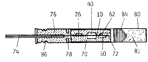
Figure 4 shows a finished detonstor containing a firing
unit with a holding fixture 70 surrounding a flexible film 10
with mounted resistors 26, capacitor 40 and chip 50 with fuse
head 62. The holding fixture 70 i8 essentially cylindrical
with a diameter of 6 mm, has a dividing plane in the plane of
the film surface 10 and, in the dividing plane, recesses for
fitting, essentially free of play, arouDd the components on
the film. A channel 72 is arranged between the fuse head 62
and that surface of the firing unit directed towards the in-
side of the detonator. Lead wires 74 extend from that surface
of the firing unit directed away from the inside of the deto-
nator, and around these there is cast a sealing plug 76 of an
elastomeric material. The holding fixture 70 is cast in poly-
,, , ' - ~ ': '
.~
1322~g
styrene and is joined mechanically to the plug 76 at 78. The
firing unit is introduced into a detonator 80 with a base
charge 82 of, or example, PETN and a primary explosive
charge 84 of, for example, lead azide located on top thereof,
in which connection the front part of the firing unit is
placed at a distance of approximately 2 mm from the primary
explosive and the detonator is sealed with grooves 86 around
the ~ealing plug 76.
. . .
- :--: .: ~ . ,- ~: