Note: Descriptions are shown in the official language in which they were submitted.
~323072
.
BIPHASIC PULSE GENERATOR FOR AN
IMPLANTABLE DEFIBRILLATOR
- The present invention relates, generally, to the field
of automatic implantable defibrillators. In such implantable
defibrillators, the defibrillation pulse is stored and
. .
delivered by a high voltage capacitor; this capacitor is short
circuited in order to terminate the defibrillation pulse.
A majority of defibrillators, found in the prior art,
are short circuiting the charged capacitor which is a waste of
energy. This energy could easily be applied to the
fibrillating heart. Also, by short circuiting the charged
capacitor, a significant amount of electrical stress is
absorbed through the electronic parts of the defibrillator
circuit. This electrical stress shortens the life of these
parts.
One attempt to use the wasted energy of the capacitor
is by using triphasic wave defibrillation. U.S. Patent No.
4,637,397 to Jones et al discloses a defibrillator that uses a
- 1323~2
flrst condltlonlng pulse, followed by ~ econd pulse of opposlte
p~larity used for defibrillating, and finally a thlrd pulse
having the same polarization as the first pulse.
However, although the Jones device uses wasted energy
of the charged capacitor,there ls a need to dellver more energy
stored ln the charyed capacltor to the fibrillating heart and
thus, lower defibrillation energy requirements.
It is therefore an object of the present invention to
obviate or mitigate the above-mentioned disadvanta~es.
According to the present lnventlon, there ls provlded a
A circuit for generating a biphasic pulse to
restore rhythm to a fibrillating heart, said circuit comprising:
capacitor means for providing a voltage to restore
rhythm to a fibrillating heart;
thyristor means, connected to said capacitor means,
for regulating said voltage;
first electrode means, connected to said thyristor
... . . .
means, for receiving and applying said regulated voltage to
said fibrillating heart;
second electrode means, connected to said thyristor
means, for receiving and applying said regulated voltage to
said fibrillating heart;
output sensing means, connected to said thyristor
means and one of said electrode means, for sensing an
exponential decay of said regulated voltage and providing a
sensed signal corresponding to said sensed exponential decay;
and
control circuit means, connected to said output
sensing means, for controlling said thyristor means and the
voltage applied to said fibrillating heart by said first and
second electrode means.
-- 2 --
. ~ . . .. .. . .
- - ~- ,. , . :. .
, ~ , , . ~ -
-- ~ . : . - ,.
1323072
The present invention provides advantages in that the
need to short circuit the high voltage capacitor is eliminated.
Thus, the stress on electronic parts is reduced. Additionally,
the energy in the high voltage capacitor that was previously
wasted is provided to the heart in the reverse direction, thereby
reducing overall defibrillatlon energy requirements.
These, together with other objects and advantages
which will become subsequently apparent, reside in the details
of construction and operation as more fully hereinafter
described and claimed, reference being had to the accompanying
drawings forming a part hereof, wherein like numbers refer to
like parts throughout.
Fig. 1 shows a biphasic defibrillation pulse from a
single capacitor as delivered from a circuit for restoring
rhythm to a fibrillating heart;
.,
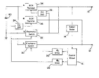
Fig. 2 shows a block diagram of a circuit for
restoring rhythm to a fihrillating heart; and
Fig. 3 shows a schematic drawing of the circuit
shown in Fig. 2.
. .; , :
1323072
Referring to the figures, the circuit of the present
invention is designed to deliver a biphasic defibrillation
pulse from a single capacitor as shown in Fig. 1. The voltage
at peak 1, or Vpkl, is equal to 25 to 1000 volts delivered to
the heart. After reaching Vpkl, the voltage will e~ponentially
decay until an SCR thyristor is turned off and the high voltage
side of the charged capacitor is steered to the other
electrode. Now, Vpk2 is delivered to the heart in the reverse
direction and is equal to 50 to 95~ of Vpkl. Thus, the short
circuiting of the high voltage capacitor is eliminated.
Fig. 2 shows the biphasic pulse generator block
diagram. Control circuit 16 is a simple Four State Sequencer
specifically designed to provide wait 1, phase 1, wait 2, and
phase 2 states by monitoring the capacitor voltage and
providing timed stimulation to the electronic switches via
circuits 20 and 22. ~hen drive circuit 20 is set high, the
electronic switch 30 is allowed to conduct and thyristor 34 is
turned on from drive circuit 20. ~t this point, the charge
stored across capacitor 40 is delivered to the heart across
. .
.~
" . ~:
- , , ~ ... . -
. . ~ ,. .
~2~2 ~,
electrodes 10 and 12 in a first polarity. After a short period
of time, sensed by circuit 14, drive circuit 20 is forced low
turning off electronic switch 30 and SCR 34. After a short
delay, less than 500 microseconds generally irldic~ted by
numeral 15, drive circuit 22 is set high turning on electronic
switch 32 and SCR 36 thus, providing an opposite current
through the heart. After another period of time sensed by
circuit 14, the electronic switch 32 is turned off which turns
off SCR 36.
In other words, the electronic switch 30 conducts to
steer the low voltage side of the main storage capacitor 40 to
electrode 12 while the high side is connected to electrode 10.
Electronic switch 32 conducts to steer the low voltage side of
the main storage capacitor 40 to electrode 10 while the high
side is connected to electrode 12.
The SCR thyristor 34, when switched "on", provides the
high voltage to electrode 10. The SCR thyristor 36, when
switched "on", provides the high voltage to electrode 12.
Output sense circuit 14 monitors the output to
electrode 10. When the output voltage at electrode 10 falls to
a suitable low level, the output sense circuit 14 will signal
the control circuit 16, which then forces drive circuit 20 to a
low. This shuts off electronic switch 30 and, therefore, SCR
thyristor 34. When the output voltage to electrode 10 falls
still further, the output sense circuit 14 signals the control
: ~ :
23a~2 _~
circuit 16. This forces drive circuit 22 to be switched to a
low, which shuts off electronic switch 32 and, therefore, the
SCR thyristor 36.
The high voltage isolation transformers 24 and 26 are
used to isolate the SCR system drive circuits and prevent the
transmission of undesired currents to them. Also, the high
voltage isolation transformers are used to separate one section
of the system from undesired influences of the other sections.
Referring to the detailed schematic shown in Fig. 3,
the operation of the system is as follows. The drive circuit
20 is set high (about 10 volts~ which allows the electronic
switch 30 shown as an insulated gate transistor Q4 to conduct
when the silicon controlled rectifier Q5, thyristor 34, is
turned on from the drive circuit 20. There is a 20 microsecond
delay through the network preceding the Schmidt trigger
circuits ICl and IC2 to allow switch 30 to be completely on
before thyristor 34 is fired. This results in the high voltage
side of the main storage capacitor 40 being switched to
electrode 10 while the low side is connected to electrode 12.
Now the high voltage Vpkl is delivered to the heart.
When the output voltage falls to a suitable low level,
the drive circuit 20 is set low, turning off electronic switch
30 as shown as an insulated gate transistor Q4 and, therefore,
the SCR thyristor 34.
- 6 -
.
.. ..
, ~
~ 1323072 -~
Next, after a 500 microsecond delay and drive circuit
20 has gone low, drive circuit 22 is switched to a high (i.e.,
approximately 10 volts). This allows electronic switch 32
shown as an insulated gate transistor Q3 to be operational and
silicon controlled rectifier thyristor 36 is fired by its
nominal 20 microsecond delay circuit (IC3-4 and network). The
delay is again necessary to allow switch 32 to be fully on
before SCR 36 is fired. The Schmidt trigger circuits IC3 and
IC4 are for squaring the pulses for good logic operations. The
process steers the high voltage side of capacitor 40 to
electrode 12 and the low voltage side of capacitor 40 to
electrode 10. Therefore, the voltage to the load is reversed
and the high voltage Vpk2 is delivered to the heart.
As soon as the voltage falls to another low level,
drive circuit 22 will be forced to a low and shut. off
electronic switch 32 shown as an insulated gate transistor Q3.
Therefore, the SCR Q6 thyristor 36 will also be off.
Drive circuit 20 and drive circuit 22 are derived from
a simple electronic sequence circuit which incorporates a chip
such as the 14017B manufactured by ~otorola. These circuits
are also used to monitor the main capacitor voltage.
The foregoing is considered as illustrative only of
the principles of the invention. ~urther, since numerous
modifications and changes will readily occur to those skilled
in the art, it is not desired to limit the invention to the
. .. , -, . ... . ~ - . ~ . .
.: : . . ~ : : , . .: .: ; ; ~ .. : . . . . :
: . :: :: :: . . :
, . .. : , , :
.~. : - ,.~ . : .
exact construction and operation shown and described, and
accordingly, all suitable modifications and equivalencies may
be resorted to, falling within the scope of the invention. One
such modification is that the electronic switches 32 and 30
shown in Fig. 3 as insulated gate transistors, could also be
power field effect transistors or high voltage bipolar
transistors. The block diagram emphasizes the generalities by
illustrating the central idea of the circuit without reference
to specific circuit elements. It is, therefore, the intent
that the present invention not be limited to the above but be
limited only as defined in the appended claims
~' , ' '`:' '; :