Note: Descriptions are shown in the official language in which they were submitted.
1 323~57
TED/3470 ¦~
PCM COMMUNICATION SYSTEM
The present invention concerns digital data transmission
systems.
In the realm of digital communications, the use of binary
digits, commonly known as "bits", where each symbol is allowed to take
one of only two values, is widespread. For certain applications,
sets of eight bits are grouped together as a "byte"~
In order to transmit several identical channels over a
single, higher rate, bearer, it is also common practi~e to "bit
interleave" ~he bits fro~ each channel, although recently some
national and international standards have suggested that byte
interleaving" should be used. In this case, the high rate bearer
carries 8 consecutive bits from the first input channel, followed by 8
consecutive bits from the second, and~so on. It is axiomatic that
byte interleaving uses e1ght timæs as~much~storage (for example,
D-type bistables) as does bit interleaving for the same type of basic
processing.
,
,
.
: . , :
: , . , , :
., , ~ , . .
, . '
.
.- .. :
.
1 323457
20305 1287
The present invention is concerned with reducing the
amount of processing which has to be performed at the higher rate
in order to achie~e byte interleaving.
Accordingly the present invention consists of digital
communication apparatus for inkerleaving multiple bi~ sequences of
a predetermined length from a plurality of input signals, each
carrying multiple-bit, sequence oriented daka, all at one rate, to
a single output data system a~ a higher rate, the appara~us
comprising: for each input signal, a first array of storage means
for storing sequentially in series each multiple bit se~uence of
predetermined length, said first arrays being arranged in
parallel, each said first array including a plurality of serially-
connected flip-flops egual in number to the number of bits in each
said bit ~equence; means for reading in parallel each of said
stored bit sequences in said first arrays into second arrays of
storage means so that the bits of said stored sequences are
interleaved, each said second array including a plurality of flip~
flops connected in series by first sets of gates, the number of
flip-flops in each said second array being equal to the number of 20 bits in said bit sequence;and means for combining the sequences
output from said second arrays in such a manner that t~e output
data stream contains said multiple bit sequences input to æaid
first arrays in parallel interleaved so that, in the single final
output stream, a multiple bit sequence from one input signal is
separated from the next mul~iple bit sequence of that signal by
multiple bit sequences from each of the other input signals.
In order that the invention may ke more clearly
understood an embodiment thereof will now be described by way of
B example and with referènce to the accompanying drawings, in which:
Flgures 1 and 2 are block diagrams illustrating two
known methods of bit interleaving;
Figure 3 is a block diagram of a known method of byte
interleaving;
Figure 4 is a block dlagram of one embodlment of
apparatus according to the preæent invention for byte
interleaving, and
r~ 2
~,~, . . . .
.
1 323~57
20305-1287
~, Figure 5 is a block diagram of a modification of the
embodiment of Figure ~
Figures 1 and 2 show two known methods for bit
interleaving.
In Figure 1 four input streams IN1 to IN4 are to be bit
interleaved. Each stream is supplied to one input of an
individual D-type bis~able Q1 to Q~ The other inputs of the
bistables are supplied wi~h a clock signal C~ derived from a main
clock C1 by a divide-by-4 circuit 40. Signal C1 is a~ the output
bit rate.
. r~ 2a
,:
- .:
` ~ ,, ' . '
.
,
.
1 323~57
20305-1287
Circuit 40 also provides a signal cc and its inverse cc which
appear at the trailing edge of the pulses of C4. The outputs of
bistables Ql-Q4 are taken to an array 30 of NOR-Gates and serially
connected bistables.
Thus the output of bistable Q4 is taken to one input of
a similar bistable 11 which is clocked with signal C1. The output
of bistable ll is taken to one input of a NOR-Gate 12 the other
input of which is connected to signal cc. The output of bistable
Q3 is taken to one input of a NOR-Gate 13 the other input of which
is connected to signal cc and the outputs of gates 12 and 13 taken
to a NOR-gate 14 the output of which goes to one input of a
bistable 15 clocked, like bistable ll, by s:ignal C1. The output
of bistable Q2 is combined with the output of bistable 15 in the
same way as the outputs of bistables Q4 and 11, that is they are
applied to respective NOR-Gates 17, 16 cloclced by signals cc and
cc and the outputs of which are taken to another NOR-Gate 18
providing an input to a bistable l9 clocked by signal C1. The
final bit interleaved output signal is OUtpllt by a bistable 20
also clocked by Cl and coupled to the outputs of bistables Q1 and
19 by NOR-Gates 21, 22, 23 all of which funrtion in a manner
similar to that of the previous two sets of NOR-Gates. This may
be summarized as parallel loading when cc is low, and serial shift
when cc is low.
In the embodiment of Figure 2 the outputs of the four
bistables Ql to Q4 are taken to an array 31 of respective NOR-
Gates 32,33, 34, 35, the NOR-Gates being supplied w1th signals
CCl, CC2, CC3 and CC4 from the divide-by-4 circuit 40.
.~ 3
3234 5~7
20305-1287
The outputs of the four ~OR-Gates are taken to a four
input NOR-Gate 36 the output of which is taken to a bistable 37
clocked by signal Cl.
The method of Figure 2 has the advantage over that of
Figure 1 of using less bistables, but the d:isadvantage of uslng a
4 input gate 36. In the general case of N iinputs, it would use an
N input gate if this scheme were followed exactly, but variations
are possible to reduce the number of inputs per gate at the
e~pense of using more gates and more bistables. The timing
diagrams appended to Fiigures 1 and 2 show only nominal times for
illustrative purposes.
:
:
`: :: : :
3a~
:
~ 32~57
Figure 3 shows a known method for byte interleaving, using
principles similar to those of Figure 1; it has been assumed that the
input streams INl-IN4 are already byte synchronised, and that there is
a means of synchronising the divide-by-3 circuit to the byte timing.
In all cases the methcds are shown with 4 input channels as an
example.
In the embodiment of Figure 3 the singte D-type bistables Ql
to Q4 are replaced by four arrays or banks of serially linked
bistables, these being Ql to Q8 for input IN1, Q9 to Q16 for input IN2
and so on. All these bistables are clocked by signal C4. Thus when
a complete byte has been received from each input the first bit of the
INl s;gnal will be stored at Ql, the second at Q2 and so on.
Similarly for lN2 the first bit will be at Q9, the second at Q10 and
so on.
In order to simplify the drawing additional circuit elements
associated with the arrays of bistables are only shown with respect to
the IN4 signal paths. These additional elements consist of an array 50
of 32 D-type bistables all having their clock inputs connected to the
~LC~,~
Cl~signal ~u~t. Furthermore the output of each of the bistables in --
the four originally described arrays are each connec~ed to the input
of an individual NOR-Gate 51 save for the output of bistable Q32 which
is connected directly to the input of the 32nd bistable in array 50.
Each bistable in array 50 is, apart from the output bistable,
associated with three NOR-Gates in a-manner totally analagous to the
NOR-Gates shown in Figure 1. The NOR-Gates arle indicated at 52 and
the first pair of NOR-Gates in each set of three are respectively
connected to signals cc and its inverse cc generated by a divide-by-8
circuit 53 operating on signal C4.
A method for byte interleaving, using principles similar to
those of Figure 2 is obvious, but is not given in detail here.
The practical realisation of logic processing circuits
involves the correct tolerancing of the timing delays of the various
logic elements, including allowance for the set-up and hold times of
the D-type bistables. In particular, the tolerancing of all the
foregoing circuits requires that the permitted delays of all the
elements shown in-~herfigures~are related to the output symbol rate,
that-~t, to the shortest repetition period.
. -- ,
~ 3~5~
20305-1287
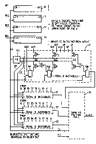
In the case of byte interleavlng, :lt would be an obvious
advantage if the amount of processlng whlch ]las to be performed to
meet thls crlterlon could be re~uced. Flgure 4 shows the prlncl-
ple used to achleve this, namely that the blts oE the input chan-
nels are interchanged, using logic processes whose timing toler-
ances are related only to the input rate, ~e:Eore belng ~inally blt
interleaved using simple circultry like that of Figure 1 or 2
The stages ln the byte stores have been numbered in reverse order,
to lllustrate the sequence of the ~its in eac~ input channel and
10 in the output channel.
As can be seen in Figure 4 each of the lnput signals
INl-IN4 is fed into a respective array or block of 8 D-type bist-
ables, the arrays belng numbered 10,11,12 and 13. Each array then
stores a byte with the flrst bit loaded of channel INl lndlcated
at Ql, the second bit of INl at Q2 and so on. Similarly the first
blt of IN2 is indlcated at Q9. Each of these arrays ls identlcal
to the array Ql to Q8 shown ln Flgure 3. However ln khls embodi-
ment the contents of blocks 10-13 are fed ln parallel lnto four
addltlonal circuit arrays or blocks 90-93. Only block 90 is shown
20 in detail as blocks gl, 92 and 93 are ldentical ko lt. Block 90
consists of an array of 8 D-type bistables 101, 102, ... 108 (only
three are shown). The block also lncIudes seven sets of NOR-Gates
lll to 118, each set conslsting of three NOR-Gates connected in
exactly the :ame manner as the NOR-Gates and blstables ln Figures
1 and 3, the first pair of NOR-Gates in each sek bein~ respectlve-
ly supplled wlth a slgnal cc and lts lnverse cc taken from a
dlvlde-by-8 counter 120. A: is ~hown in Figure 4 the fir:t NOR-
~
` X! :~ :
:
.
' .
~ 3 ~ 3 !~
20305 12~7
Gate of set 118 recelves the output of blstable Ql, the flrst NOR-
Gate of Set 112 the output of blstable Q21 and so on tlll the
first NOR-Gate of set 111 receives the output of blstable Q29 of
array 13. All these flrst NO~-Gates receive slgnal cc at their
other lnput. The second NOR-Gate of each set receives signal cc
at one input and the output of the precedlng blstable ln the
block.
The result of thls operation ls that block 90 holds the
8 blts Ql, QS, Q9, Q13, Q17, Q21, Q25 and Q29, block 91 the blts
Q2, Q6 etc. The bits from the four input channels have thus been
lnterleaved in a particular order. The contents of the four
blocks 90-93 are then read out
~ '
.
1 323457
20305-1287
and interleaved by a circuit 20 iden-tical to either of the entire
circuits shown in Figures 1 or 2. It will be seen that the
interleaving of the bits in the four blocks followed by the
interleaving of the outputs of the blocks ef.fectively byte
interleaves the four input data channels.
As a further but not exclusive eY~ample of this
principle, Figure 5 shows the bit interchange method which may be
used in order to achieve effective byte interleaving for 16 input
channels, using bit interleaving in two stages to achieve the
final rate.
The embodiment illustrated in Figure 5 has 16 arrays
201-216 each associated with a single incom:ing signal INl-IN16.
Each of these arrays is identical to the array of 8 serial-
connected bistables Ql to Q8 shown in Figure 3 and to the arrays
10 to 13 shown in Figure 4. The parallel ou-tputs of these blocks
201-216 are taken to 16 arrays 221-236 each identical to the
blocks 90-93 shown in Figure 4. The manner in which the incoming
bits are arranged in these arrays 221~236 is shown by the number
grids.
The serial output of the last bistable in each array
221-236 is taken to one of four arrays 240-243 each of which is
effectively identical to either the entire circuit~shown in Figure
1 or in Figure 2.
The outputs of each of the arrays 240-2~3 are taken to:a
slngle array 250 which is identical to the array 240. As will be
appreciated the successive bit interleaving of the input signals
eventually results in the final output signal being byte
:
~ , . , , `
.
' ' ..'' ' ' ' '',', ' :
.
1 32345~
20305-1287
interleaved.
The foregoing description has been concerned with the
interleaving bytes of incoming signals. It will be appreciated
that the basic principles of the apparatus described with
reference to Figures 4 and 5 could be applied to multiple bit
sequences of lengths other than 8.
6a
.