Note: Descriptions are shown in the official language in which they were submitted.
132359~ 27598-42
1. Field of the Invention:
The present invention relates to a dielectric block
plating process for forming a plated layer through an electrolytic
plating process over the surface of a dielectric block having
through holes extending from the bottom surface to the top surface
thereof, and a plating apparatus for implementing the dielectric
block plating process.
2. Description of the Prior Art:
Generally, the dielectric block plating process for
forming a conductive layer comprises the following steps.
1) washing and roughening the surface of a dielectric
block made of ceramic material comprised of TiO2 and BaO,
2) coating the surface of the dielectric block with a
conductive base layer through an electrolyess plating process,
3) coating predetermined portions of the surface of
the dielectric block which are not to be coated with an upper
conductive layer with a resist material,
4) coating the surface of the dielectric block with an
upper conductive layer through an electroplating process, and
5) removing the resist material and the conductive
base layer coated with the resist material.
When the dielectric block is plated through the
foregoing dielectric block plating process to manufacture a
dielectric filter having inner conductors in the through holes and
an outer conductor at the surface thereof, the electrolytic
solution is liable to stagnate in the through holes of the
, ,~
. . .
.
:
1 3 2 3~l9~ 27598-42
dielectric block and hence, the surfaces of the through holes may
be coated with inner conductive layers having an insufficient
thickness. The electric characteristics of such dielectric filter
containing inner conductive layers (inner conductors) having an
insufficient thickness thereof, do not meet desired electric
characteristics.
There is a dielectric block plating process invented to
solve the foregoing problem in Japanese Patent Laid-Open
Publication No. 59-185795, published October 22nd, 1984. This
conventional dielectric block plating process requires a plurality
of electrolytic solution injecting means to be disposed `~
respectively adjacent and opposite to the through holes of a
dielectric block. Accordingly, this dielectric block plating
process requires the dielectric block being set exactly at a
predetermined position adjacent to the electrolytic solution
injecting means.
~ nother conventional dielectric block plating process
employs auxiliary anodes, which are respectively inserted in the
through holes of a dielectric block to form inner conductors
having a sufficient thickness.
SUMMARY OF THE INVENTION
Accordingly, it is an objective of the present invention
to provide a dielectric block plating process and a dielectric
block plating apparatus for implementing the dielectric block
plating process capable of forming conductive layers having a
uniform thickness over the surfaces of a dielectric block.
'', . '' ' ~
:
1323~ 27598-42
It is another object of the present invention to provide
a dielectric block plating apparatus having a simple construction.
It is a further object of the present invention to
provide a dielectric block plating apparatus capable of
satisfactorily coating the surfaces of the through holes of a
dielectric block with conductive layers without exactly
positioning the through holes respectively adjacent and opposite
to each of a number of electrolytic solution injecting means for
injecting the electrolytic solution into the through holes of the
dielectric block, and inserting auxiliary anodes in each of the
through holes of the dielectric block.
It is still a further object of the present invention to
provide a dielectric block plating apparatus suitable for
automation.
In one aspect of the present invention, a dielectric
block plating process for forming a conductive layer through an
electroplating process over the surface of a dielectric block
having a plurality of through holes extending from the top surface
to the bottom surface thereof, said holes having center axes
extending in a vertical direction and coated with a conductive
base layer formed by an electroless plating process in a plating
tank filled with an electrolytic solutlon comprises steps of:
(1) immersing the dielectric block in the electrolytic
solution contained in the plating tank;
(2) circulating the electrolytic solution through the
plating tank so that the electrolytic solution will flow in the
direction of the center axes of the through holes;
. ~, ,
. ~ ~
,,, :: ~ ,
~ ~ .
~323~
27598-42
(3) applying a negative voltage to the conductive base
layer;
(4) applying a positive voltage to the electrolytic
solution; and
(5) when the plating process is complete, removing the
dielectric block from the electrolytic solution.
In another aspect of the present invention, a dielectric
block plating apparatus for forming conductive layers over the
surface of a dielectric block having a plurality of through holes
extending from the top surface to the bottom surface thereof, sald
holes having center axes extending in a vertical direction and
coated with a conductive base layer formed by an electroless
plating process in a plating tank filled with an electrolytic
solution comprises:
(1) holding means for holding the dielectric block
within the electrolytic solution in an orientation with the axes
of said through holes extending in a vertical directlon;
(2) electrolytic solution circulating means for
circulating the electrolytic solution under pressure through the
plating tank;
(3) means for controlling the flow of the electrolytic
solution so as to flow in the direction of the axes of the through
holes;
(4) voltage applying means for applying a negative
voltage to the conductive base layer formed on the dielectric
block; and
(5) voltage applying means for applying a positive
:
1~23~
27598-42
voltage to the electrolytic solution, said positive voltage
applying means being positioned within said plating tank to face
and confront entrances of the through holes in the block when the
block is held in said orientation by said holding means.
The above and other objects, features and advantages of
the present invention will become apparent from the following
description taken in conjunction with the accompanying drawingæ.
BRIEF DESCRIPTION OF THE DRAWINGS
Figure 1 is a perspective view of a dielectric block;
4a
. .
132359~
27598-42
Fig. 2 is a sectional view taken on line 103-103 in Fig.
l;
Fig. 3 is a sectional view of a dielectric block plating
apparatus, in a preferred embodiment, according to the present
invention;
Fig. 4 is a fragmentary cutaway perspective view of the
dielectric block plating apparatus of Fig. 3;
Fig. 5 and 6 are perspective views of assistance in
explaining the construction of an electrolytic solution supply
unit incorporated into the dielectric block plating apparatus of
Fig. 3;
Fig. 7 is a perspective view of a holding device for
holding a dielectric block; and
Fig. 8 is a side elevation of the holding device holding
a dielectric block.
DESCRIPTION OF THE PREFERRD EMBODIMENT
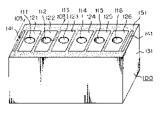
Referring to Figs. 1 and 2, a dielectric block 100
formed of a ceramic material containing TiO2 and BaO has through '
holes 111 to 116 extending from the top surface to the bottom
/ surface thereof. Conductive collar/!d areas 121-126 for adjusting
/ the capacitance of the dielectric block 100 are formed in the top
/ surface of the dielectric block respectively around the edges of
the through holes 111 to 116. Also formed in the top surface of
the dielectric block 100 are electrodes 141. Indicated at 151 is
a nonplated area in which no conductive layer is formed. An outer
conductor 131 is formed in the side surfaces of the dielectric
~ ~ . , - - - -
,: ,'
~32 3Sj~ 27598-42
block 100. As best shown in Fig. 2, inner conductors 121 to 126
are formed respectively over the surfaces of the through holes 111
to 116. The inner conductors 121 to 126 are connected
electrically to the outer conductor 131 by a bottom conductor 161.
Referring to Figs. 3 and 4 there is shown a preferred
embodiment of a dielectric block plating apparatus according to
the present invention. A plating tank 401 is filled with
;~ ~
an electrolytic solution. T ~3~i3e~e~c~ric block 100 is
immersed in the electrolytic solution in the plating tank
401 for electrolytic plating. The electrolytic solution
is pumped for circulation through the plating tank 401 by
a pump 402. The electrolytic solution, for example, for
silver plating contain~ KAg(CN) 2 and KCN. The
electrolytic solution pumped by the pump 402 is supplied
into the plating tank 401 through a supply pipe 403, such
as a vinyl chloride pipe, connected to a pipe joint 408
connected to the bottom of the plating tank 401 so that
the electrolytic solution will overflow the plating tank
401. The electrolytic solution overflows the plating tank
401 into a sump 404 formed around the plating tank 401
between the walls of the plating tank 401 and an external
casing. A return pipe 405 has one end connected to the
bottom of the external casing and the other end connected
to the pump 402. The overflow electrolytic solution
contained in the sump 404 is returned through the return
pipe 405 to the pump 402. Preferably, a filter unit 407
is provided in the return pipe 405.
Flow control devices for forming a uniform flow of
the electrolytic solution within the plating tank 401 will
be described hereinafter.
In Figs. 3 and 4, the flow control device is embodied
in a flow control plate 409 having small perforations 410.
The perforations are distributed over the entire area of
the flow control plate 409. The electrolytic solution
.
1323~i9~
supplied through the supply pipe 403 into the plating tank
401 is distributed uniformly by the flow control plate
409, so that a substantially uniform flow of the
electrolytic solution is formed within the plating tank
40~.
/ In Fig. 5, the flow control device is embodied in a
manifold formed by branching the free end of the supply
pipe 403 into a plurality of branches on the bottom wall
of the plating tank 401. A plurality of through holes 410
are formed in the manifold to spout the electrolytic
solution uniformly therethrough into the plating tank 40~.
In Fig. 6, the flow control device is embodied in a
zigzag pipe formed by bending the free end of the supply
pipe 403 in a zigzag shape on the bottom wall of the
plating tank 401. A plurality of through holes 410 are
formed in the 2igzag pipe to spout the electrolytic
solution therethrough uniformly into the plating tank 40~.
The perforated plate, the manifold and the zigzag
pipe are equivalent to each other in the effect of forming
a uniform flow of the electrolytic solution within the
plating tank 401.
Anodes 420 for applying a positive voltage to the
electrolytic solution are arranged within the plating tank
401. Each anode 420 is, for example e~ silver plating, a
rectangular plate formed of pure silver. The anodes 420
are fixed to an anode holding structure 421, such as a net
or a cage, formed of Ti as shown in Figs. 3 and 4. The
`` 1323~
anode holding structure 421 holding the anodes 420 is
fixedly placed within the plating tank 401.
Referring to Figs. 7 and 8, a holding device 430 for
holding the dielectric block 100 within the plating tank
401 to immerse the dielectric block 100 in the
electrolytic solution is formed of a material which will
not dissolve in the electrolytic solution and in a
solution for removing a material plated over the surface
of the holding device 430, for example, a stainless steel
material or piano wires. The holding device 430 comprises
a frame 701, a pair of grippers 702 for gripping the
dielectric block 100, and a spring 703 biasing the pair of
grippers 702 so as to grip the dielectric block 100
therebetween. The pair of gripperfi 702 are supported on
the frame 701. When the pair of grippers 702 are formed
of a resilient material in a shape capable of holding the
dielectric block 100 therebetween, the springs 703 need
not be provided. The respective pairs of grippers 702 are
closed when no dielectric block is held therebetween. In
holding the dielectric block 100, the pair of grippers 702
are opened to receive the dielectric block 100
therebetween aæ shown in Fig. 8. The pair of grippers 702
are connected electrically to the frame 701, so a voltage
applied to the frame 701 can be applied to the ~u~
.~`, `,~ b~ se
-`~ conductivellayer over the surfaces of the dielectric block
100 .
Thus, a positive voltage is applied to the anodes 420
- ` 1323~
and a negative voltage is applied to the ground conductive b~
layer formed over the surface~ of the dielectric block
100. Thereby an upper conductive layer is formed over the
bc~se
predetermined area of the ~*d conductive/layer.
Although the invention ha~ been de~cribed in its
preferred form with a certain degree of particularity,
obviously many changes and variations are possible
therein. It is therefore to be understood that the
present invention may be practiced otherwise than
specifically described herein without departing from the
scope and spirit thereof.
.0
:
:: . ~: