Note: Descriptions are shown in the official language in which they were submitted.
3 '`~ ~ ~
The present invention relates to a thin image
display apparatus using a plurality of cold cathodes.
Fig. 1 is a partial sectional view of an image
display apparatus according to an embodiment of the present
invention.
Fig. 2 is a sectional view of the essential parts
of an electron source section according to the same
embodiment.
..
Fig. 3 is a plan view schematically showing an
electrode arrangement according to the same embodiment.
Fig. 4 is a perspective view of the essential parts
of two-dimensional electron sources as configured according
to another em~odiment of the present invention.
.~
Figs. 5A and 5B are a perspective view and an
enlarged perspective view of the essential parts respectively
of a matrix display apparatus of electric field emission type
related to the present invention.
,
A number of thin display apparatuses comprising a
plurality of cold cathodes arranged two-dimensionally for
displaying an image using X-Y matrix electrodes have been
disclosed in the related art. Among them, a thin image
display apparatus using a cold cathode of electric field
emission type is closely watched. This thin display
apparatus, as shown in Fig. 5A, has a substrate with the
', 25 surface thereof formed of a plurality of cold cathodes of
.~! thin film field emission type in a density as high as lo6 to
'.'! 107 units~cm. As shown in Fig. 5B, these cathodes make up an
-- 1 --
~.
~`~
,
:' ' ,
." ~
;~ :
~323`t~ ~
X electrode 22 as one part of the matrix electrodes on the
surface o~ a substrate 21, on which a ~ electrode 2~ is
formed as the other part of the matrix electrodes together
with an insulating layer 23. A minute aperture 25 one ~m to
1.5 ~m in diameter is formed in the Y electrode at each
inter-section of the X-Y electrodes, and the insulating layer
23 is etched. A substrate assembly thus formed is rotated,
while high a melting point metal such as tungsten or
molybdenum is diagonally deposited by evaporation thereby to
form a conical cold cathode chip 26. After forming cold
cathodes, the unrequired metal layer
- la -
,~
: . :
' ~ - ' , . : ~ . .
,: ~ : . . : , ~ -
~3'~ 3 `' ~ 3~.
in the surface is removed to produce a plurality of electron
sources of cold cathodes of thin film field emission type.
These X Y matrix eleckron sources are arranged in
opposed r~lationship with a face plate 27 coated with a
phosphor material 28 to configure an image display apparatus.
This image display apparatus, which comprises as many as
more than 1000 minute electron sources in each pixel,
generally has a uniform characteristic in spite of possible
variations in the characteristics of individual minute
electron sources, thus producing a comparatively uniform
brightness over the whole screen.
The a~orementioned image display apparatus with its
satisfactory characteristics, however, has not yet found
practical applications due to the facts that a complicated
production process makes a production cost high and that it
is difficult to fabricate uniform cold cathodes of field
emission type over an area required of a display apparatus.
Another reason is that a laminaked structure of an X-control
electrode (cold cathode) and Y-control electrode (gate
electrode) through an insulating layer therebetween leads to
a large electric capacity, resulting in a heavy load imposed
on a drive circuit.
The present invention
i
ii! 25
~i
~ 2
.. ,~ ~
,,, : .
"
.~?, ~
'`" ` ~ `" :
~3~ J '~
1 provide8a thin ima~e display apparatus comprising an
insulating substrate having two-dimensionally arranged
electron source units controlled by X-Y matrix control
electrodes and a face pla-te coated with a phosphor
material arranged in opposed relationship with the
insulating substrate wherein the said electron scorce
units corresponding to each interection of X-Y matrix
control electrodes includes a cold cathode connected to
an X-control electrode and a gate electrode connected to
a Y-control electrode opposed to the cold cathode in the
same plane, the electron source being formed in the part
; of the substrate surface on other than at least one of
the X- and Y- control electrodes.
Upon application of a voltage between the cold
cathode and the gate electrode arranged in opposed
r~lationship with each other on the same surface in the
manner mentioned above, a high electric field of
approximately lO V/cm is formed at the forward end of
the cold cathode and electrons are emitted. A part of
the electrons thus emitted enters the anode directly.
Another part of the electrons flow into the opposite
gate electrode thereby to generate secondary electrons
in the surface of the gate electrode. The secondary
electrons thus generated are accelerated by a positive
voltage (hereinafter called the "anode voltage") applied
to the phosphor face of the opposed face plate and
bombarded on the phosphor material to emit light.
The apparatus according to the present
., .
~ - 3 -
;~ .: ,, . . ~ :
.: . :
, :' ' ~'. ,
:. ~ ' -'
:,
:~323~
1 invention in which a plurality of cold cathodes of
planar field emission type are formed on the surface of
an insulating substrate defined by X-control electrodes
and Y-control electrodes, has the advantages (1) that
the electric capacity between the electrodes is extreme-
ly reduced (to 1/20 to 1/30 of the related art), (2)
that the production cost is low since cold cathodes and
gate electrodes are capable of being formed at the same
time, and (3) that crosstalks are very small.
i. . .
, .~ ~ . .
,
A partial sectional view of an image display apparat~s
accordin~ to the present invention is shown in Fig. 1. The
image display apparatus comprises a glass substrate 1 having
an electron source for electric field emission at each
intersection of X-Y matrix electrod0s, and a face plate 4
coated with phosphor material in opposed relationship with
the glass substrate 1. The glass substrate 1 has cold
cathode 2 and gate electrodes 3 arranged face to face on the
surface. When a positive voltage of, say, 100 V is applied
to the gate electrodes 3 with respect to the cold cathodes 2,
electron beams 7 are emitted. A part of electrons thus
emitted flows into the gate electrodes 3, while the other
part is accelerated by a high voltage of, say, 500 ~ applied
to an anode 5 and hits a phosphor surface thereby to cause
the phosphor to emit light.
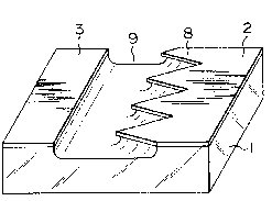
An enlarged perspective view of an electron source is
shown in Fig. 2. A multiplicity of sawtoothed protrusions 8
are formed in the surface of the cold cathode 2 opposed to
the gate electrode 3. Further, the surface of the glass
substrate 1 has a recess 9 between the cold cathode 2 and the
, gate electrode 3 to facilitate formation of a high electric
field at the forward end of the cold cathode 2.
~! Fig. 3 shows a part of electrode arrangement. X-control
! electrodes X1, X2, X3, .... Xn and Y-control electrodes Y1,.,
~, 25 Y2, Y3, Yl~ make up matrix control
..~
~ - 5
~, ,~.
.i
.; ~ .
, ~
1 electrodes. A plurality of electron sources 13 are
formed on the substrate surface defined by these control
electrodes. Each electron source 13, which is con-
figured as shown in Fig. 2, includes a cold cathode 2
connected to an X-control electrode and a gate electrode
3 connected to a Y-control electrode.
Thls construction of the electron sources 15
not overlaid on the X or Y-control electrodes is a
reduction of 1j20 to 1/30 of the area required by the
prior art for superposing the electrodes on each other
through an insulating layer. As a result, the
probability of short-circuiting between electrodes due
, .
to a pinhole in the insulating layer and the electric
capacity are decreased to 1/20 to 1/30.
, 15 Now, a method of fabricatig two-dimensional
-~ electxon sources will be explained. A film o such a
metal as nickel is deposited by evaporation to the
i thickness of 0.5 ~m over the whole surface of the glass
-~ substrate, and formed in stripes by photolithographyn
Electrodes are formed to the width of 0.1 mm. An SiO2
film as thick as 1 ~m is deposited as an insulating
layex by the CVD process, and a part of the insulating
film over an X-control electrode is removed to form a
window for connecting to a cold cathode. Further, a
tungsten film i5 deposited by evaporation to the
thickness of 0.2 ~mj so that a cold cathode 2, a gate
electrode 3 and a Y-control electrode are formed
:~ simultaneously by photolithography. The Y-control
. ~ .
~ 6 -
, ...
:.~
,~: . , - : .
~ ~;3 ~
1 electrode is made as wide as 0.5 mm.
The protrusions of the cold cathod are set at
an interval of 2 ~m from the gate electrode. There are
approximately 500 protrusions 8 per electron source unit
(which correspond to one pixel). As the next process,
the whole substrate is immersed in a buffer etching
solution to form a recess 9 at the forward end of the
cold cathode as shown in Fig. 2.
The electrode material for forming an X-
control electrode is not limited to nickel metal, butmay preferably take the form of aluminum, titanium,
gold-chromium alloy or other metal material which has a
high adhesion wi~h the glass substrate and low in
resistivity. Also, a silver electrode or a gold elec-
trode may be formed by the screen printing process orthe like. The SiO2 film used as an insulating layer may
be replaced by another material of high insulation
characteristic such as SiN, SiO or A12O3. Instead of
tungsten, on the other hand, tantalum, molybdenum or an
alloy or carbide thereof having a high melting point may
be us~d as a material of the cold cathode with equal
effect.
In this way, a glass substrate having electron
sources units 13 in the number of 480 x 660 arranged in
matrix are disposed in opposed relations wi~h a face
plate coated with a ZnO:Zn phosphor material at inter-
vals of 0.3 mm, and the surrounding parts are seal~d
with frit glass of a low melting point. The resulting
-- 7 --
, ~ . . - ~ :
:. ~ . . . . .
. : ; :,
x
.,~ . . . .
r.' ~
~ $ 2 ~
1 assembly is evacuated to produce an image display
apparatus with a screen size of 10 inches.
When a voltage of 150 V is applied to the
Y control electrodes ( video signal modulation elec-
trodes) as against the X-control electrodes (vertical
scanning electrodes), an electron emission current of
about 10 ~A is produced for each pixel. Also, upon
application of 500 V to the surface of the phosphor
material with an image displayed by line-at-a-tlme
driving method, a screen brightness of approximately 50
fL is obtained.
In place of the ZnO:Zn phosphor material used
according to the present embodiment, the three primary
~ colors of red, green and blue may be arranged in stripes
V;j 15 to produce a color image.
; An electrode configuration of a two-dimen-
sional electron source according to another embodiment
is shown as a perspective view in Fig. 4. Stripe
`, electrodes 10 having a width of 0.1 mm and thickness of
3 ~m are formed by the creen printing method on the
;~ surface of the glass substrate 1. As the next step,
frit glass of low melting point is laid to the thick-
ness of 1 ~m by screen printing at intersections of the
stripe electrodes 10 and Y-control electrodes to form an
insulating layer 12. In similar fashion, Y-control
electrodes 11 having a width of 0.05 mm and thickness of
1 ~m are ~ormed in stripes. Further, a cold cathode
material WSi2 is formed by sputtering over the whole
, ~
~, 8
..,
., . -
.,~ , . :
~, '
`~ ' ' ' ' ' ' '
` "" ~ : , ,
~ 3 2 ~.;3;~'$.~
1 surface, and cold cathodes 2 and gate electrodes 3 are~ormed at the same time by photolithograhy.
As shown in Fig. 4, the cold cathodes 2 and
the gate electrodes 3 are engaged in comb, and the sides
of these electrodes opposed to each other are arranged
in parallel to the X-co~trol electrodes (perpendicular
to the longitudinal direction of the Y-control elec-
trodss). This arrangement causes emitted electron beams
to widen somewhat along the longitudinal direction o
the Y-control electrodes but not substantially along the
perpendicular direction thereof. As a result, electron
beams are prevented from hitting the phosphor material
corresponding to adjacent Y-control electrodes, so that
what are called crosstalks rarely occur, thus producing
a high-definition image display apparatus. In particu-
lar, color mixing is effectively prevented in a color
image display apparatus configured by three-color
phosphor materials in stripes.
In this way, a glass substrate 1 making up a
two-dimensional electron source and a ~ace plate coated
with a phosphor matreial are sealed with each other in
opposed relations and evacuated in the same manner as in
the first embodiment thereby to test produce an image
display apparatus, which is capable of displaying a
clear image substantially free of crosstalks like the
first embodiment.
_ 9
: ~ . . - .:
. : ~ . - -