Note: Descriptions are shown in the official language in which they were submitted.
~V-6574
1324637
-- 1 --
LOW FRE~UENCY CURING APPARATUS APPLICABLE
.
DIRECTLY TO ORGANISM
BACKGROUND OF THE INVENTION
1. Field of the Invention
The present invention relates to a small-sized
- low frequency curing apparatus capable of providing a
required electrical stimulation to a subject such as an
organism regardless of a small capacity of a power
supply and, in particular, to a small-sized low frequency
curing apparatus which can be applied directly to the
organism and can be manufactured in the smallest possi-
ble size.
2. Description of the Related Art
Recently, use has been made of an endermicelectrical stimulation apparatus, i.e., a so-called low
` frequency curing apparatus, which can apply cenesthesic
stimulation to the skin at constant periods, and has a
small size such that it can be applied to the skin in
the form of a bandage, a poultice, and the like.
However, essentially such a low frequency
curing apparatus should be constituted so that the
electrical stimulation application mode can be changed
, to realize a stimulation effect similar to a finger-
pressure treatment such as a massage. A constant or
changeless stimulation causes a remarkable decrease in
the degree of cenesthesia, thus lowering in the effec-
tiveness of any cure. Accordingly, a small-sized low
frequency curing apparatus capable of realizing a
variety of stimulation effects is desired.
SUMMARY OF THE INVENTION
An object of the present invention is to provide an
easily handled, small-sized low frequency curing appara-
tus capable of applying a variety of cenesthesic low
frequency stimulation effects to an organism, and
employing constituent elements and members which enable
- 2 - ~32~37
the high-density mounting necessary for any reduction in
size of the apparatus.
The above-mentioned object is attained by providing
a low frequency curing apparatus comprising: a small-
sized power source; a boosted pulse generating unitconnected to the small-sized power source, for gener-
ating a train of boosted pulses; an accumulating unit
connected to the boosted pulse generating unit, for
accumulating electrical energy to at least a prede-
termined amount at which a stimulation effect for anobject to be electrically stimulated is attained; a low
frequency pulse outputting unit connected to the accu-
mulating unit, for outputting electrical energy accu-
mulated in the accumulating unit as low frequency
pulses; a pair of electrode members able to be applied
in a plane state to the object to be stimulated, for
transmitting the low frequency pulses from the low
frequency pulse outputting unit to the-object; and a
signal processing unit connected to the small-sized
power source, for carrying out a signal processing based
on a predetermined algorithm and outputting a first
pulse signal for driving the boosted pulse generating
unit and a second pulse signal for driving the low
frequency pulse outputting unit, a pulse width or a
pulse interval of the first pulse signal or second pulse
signal being changed, whereby a variety of low frequency
stimulation effects are applied to the object to be
stimulated.
BRIEF DESCRIPTION OF THE DRAWINGS
Other objects and features of the present invention
will be described hereinafter in detail by way of
preferred embodiments with reference to the accompanying
drawings, in which;
Fig. 1 is a block diagram schematically illustrat-
ing a constitution of the low frequency curing apparatus
according to the present invention;
Fig. 2 is a circuit diagram illustrating a first
~ 3 ~ 132~37
embodiment of the present invention:
Figs. 3a to 3e are diagrams showing the signal
waveform of each point in the apparatus shown in Fig. 2;
Figs. 4a and 4b are flowcharts for explaining the
operation of an example of the signal processor shown in
Fig. 2;
Fig. 5 is a block diagram illustrating a constitu-
tion of another example of the signal processor shown in
Fig. 2;
Fig. 6 is a circuit diagram illustrating a modi-
fication of the apparatus shown in Fig. 2;
Figs. 7a to 7c are diagrams showing the signal
waveform for explaining an example of the operation of
the signal processing means shown in Fig. 1;
Fig. 8 is a circuit diagram illustrating an example
of the constitution of the one-shot shown in Fig. 5;
Figs. 9a to 9d are diagrams showing the signal
waveform for explaining the operation of the circuit
shown in Fig. 8;
Fig. 10 is a circuit diagram illustrating an
example of the constitution of the select circuit 57
shown in Fig. 5;
Figs. lla and llb are diagrams showing the signal
waveform for explaining an example of the operation of
the circuit shown in Fig. 1~;
Figs. 12a to 12c are circuit diagrams illustrating
a second embodiment of the present invention;
Figs. 13a to 13e are diagrams showing the signal
waveform for explaining an example of the operation of
the circuits shown in Figs. 12a to 12c;
Figs. 14a to 14c are diagrams showing the signal
waveform for explaining another example of the operation
of the circuits shown in Figs. 12a to 12c;
Fig. 15 is a circuit diagram illustrating a third
embodiment of the present invention;
Fig. 16 is a circuit diagram illustrating a fourth
embodiment of the present invention;
~3~37
Figs. 17a to 17c are diagrams showing the signal
waveform for explaining an example of the operation of
the circuit shown in Fig. 16;
Figs. 18a and 18b, 19a and l9b, 20a and 20b,
and 21a to 21h are diagrams showing the signal waveform
for explaining a variety of output forms according to
the apparatus of the present invention;
Figs. 22a and 22b are views showing an example of
the overall construction of the apparatus of the present
invention; and
Fig. 23 is a view showing another example of the
overall construction of the present invention.
DESCRIPTION OF THE PREFERRED EMBODIMENTS
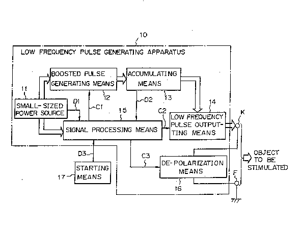
Figure 1 schematically illustrates a constitution
15 of the low frequency curing apparatus according to the
present invention.
As a fundamental constitution, the apparatus of the
present invention is constituted by a small-sized power
source 11, a boosted pulse generating means 12, an
accumulating means 13, a low frequency pulse outputting
means 14, a signal processing means 15, and a pair of
electrodes K and F. The electrode K participates in the
curing, and the electrode F does not participate in the
curing. Also, a de-polarization means 16 and a starting
means 17 are preferably added to the above constitution
in accordance with a variety of forms of implementation.
Thick arrow marks shown in Fig. 1 indicate the flow of
energy.
The small-sized power source 11 comprises a single
or a plurality of button-type batteries, sheet-type
batteries, coin-type batteries, cylinder-type batteries,
pin-type batteries and the like. Although the config-
uration of the small-sized power source is not particu-
larly restricted, a small-sized, thin-type and light-
weight battery is preferable. Also, chargeablesecondary batteries and the like can be used.
The boosted pulse generating means 12 comprises an
. . . .
.. . . .
~ 5 - 132~7
oscillator generat;.ng a train of pulses and a boosting
means consisting of, e.g., an inductor, which upon
receipt of the power supply from the power source 11,
generates a train of boosted pulses.
The accumulating means 13 comprises at least one
capacitor for accumulating boosted pulses output from
the boosted pulse generating means 12. Also, the
means 13 can include a means for detecting energy
accumulated in the capacitor, the constitution and
operation of which will be described later.
The low frequency pulse outputting means 14 com-
prises a switching means such as a transistor and the
like for transmitting the energy accumulated in the
accumulating means 13 to the electrode K or stopping the
flow of the energy.
Upon receipt of the power supply from the power
source 11, the signal processing means 15 carries out a
signal processing based on a predetermined algorithm
and, based on the processing, controls the other means.
As a fundamental control, the signal processing means 15
outputs a pulse signal Cl for driving the boosted pulse
generating means and a pulse signal C2 for driving the
low frequency pulse outputting means. Where a pulse
width or a pulse interval of the pulse signal Cl or C2
is changed based on the above predetermined algorithm,
the application mode of the low frequency output pulses
applied via the electrode K to an object to be stimu-
lated is varied. That is, a variety of low frequency
stimulation effects can be realized by suitably
selecting the pulse width and/or pulse interval of the
signals C2 and/or C2.
A chip is used as the signal processing means 15
employed in the present apparatus, the chip being
approximately 5 or 6 mm~ to 50 or 60 mm2 and having a
thickness of approximately S or 6 mm. For example, the
signal processing means corresponds to; a microcomputer
including a ROM for storing a program, a R~, a CPU and
- 6 _ ~32~3~
the like; an ASIC realizing the above program or algo-
rithm by a PLD, a gate array, standard cells and the
like; a Look-Up Table (LUT) system in which pulse
waveform data of the drive pulses is stored in advance
in a memory element and the stored pulse waveform data
is read out when needed; or a program sequencer generat-
ing the drive pulses based on a programmed algorithm; or
the like. In one embodiment of the present invention, a
general-purpose 4-bit CMOS microcomputer such as an
10 SM-500, SM-590 or SM-591 produced by Sharp Corp., is
preferably employed as the signal processing means.
The sisnal processing means is also capable of
changing the algorithm included therein to another
algorithm in response to input information given by
another constituent element, as described later in
detail.
For example, the signal processing means 15 re-
ceives input information Dl from the power source 11
and, based on an algorithm corresponding to the informa-
tion Dl, outputs the drive pulse Cl having a predeter-
mined pulse width to the boosted pulse generating
means 12. An example of the operation of the signal
processing means is shown in Figs. 7a to 7c in the form
of signal waveforms. That is, when the voltage of the
power source 11 gradually`drops (see Fig. 7a), the
signal processing means 15 outputs the drive pulse
signal C1 having a gradually increased pulse width (see
Fig. 7b). With the gradual increase of the pulse width
of the signal Cl, the boosted pulse generating means 12
outputs a boosted pulse signal so that the amplitude of
the signal is gradually increased (see Fig. 7c). An
explanation of the de-polarization means 16, starting
means 17, a control signal C3, and input information Dl,
D2, and D3, will be given by way of various embodiments.
Figure 2 illustrates a circuit constitution of a
first embodiment of the present invention. In Fig. 2, a
positive end of a power source 21 is connected to a
:,
~ 7 ~ 132~$3(
signal processor 22 and one end of an inductor 23, and
the negative end of the power source 21 is connected to
the processor and grounded. The other end of the
inductor 23 is connected to an anode of a diode 24 and a
collector of an NPN transistor 25. An emitter of the
transistor 25 is grounded and a base thereof responds to
a drive pulse Sl (signal Cl in Fig. 1~ output from the
L~ signal processor 22. A capable of the diode 24 is
connected to a collector of an NPN transistor 27 and one
end of a capacitor 26, the other end of which is
grounded. An emitter of the transistor 27 is connected
to one end of a de-polarization circuit 28 an an elec-
trode K participating in the curing process, and a base
thereof responds to a drive pulse S2 (signal C2 in
Fig. 1) output from the processor 22. The de-polari-
zation circuit 28 responds to a drive pulse S3 (sig-
nal C3 in Fig. lJ output from the processor 22, and the
other end thereof is connected to an electrode F not
participating in the curing and grounded. Reference RZ
equivalently indicates the impedance of the object to be
stimulated, i.e, organism or body.
The power source 21 comprises one or a plurality of
coin-type batteries, cylinder-type batteries, sheet-type
batteries, pin-type batteries and the like. A battery
or batteries employed in a portable apparatus such as an
IC card, a memory card, a watch and the like is pref-
erably used, as such-a battery is the smallest possible
battery available.
The signal processor 22, in accordance with a
predetermined algorithm defined by a program and the
like, can output the drive pulses Sl and S2 so that a
pulse width or a pulse interval of the drive pulses can
change with the lapse of time. Also, the processor 22
generates the drive signal S3 based on the drive
signal S2 (see Fig. 5) and supplies the signal S3 to the
de-polarization circuit 28. As a result, as will be
described later in detail, polarization charges remain-
- 8 - 132~37
ing within the organism are discharged through the
de-polarization circuit. The signal processor 22 is
provided with an input part 29 (starting means 17 in
Fig. 1) and an oscillator (OSC) 30 for generating clock
pulses. The input part 29 includes a number of switches
(SW), e.g., a switch for starting or stopping the
operation of the apparatus, a switch for selecting a
pulse output mode, and the like.
The signal processor 22 can be constituted, for
example, by a general-purpose one-chip microcomputer.
In such a case, the processor 22 will comprise a ROM for
storing a program to be executed, a RAM employed in
e~ecuting the program, and a central processing unit
(CPU) for generating the drive pulses Sl and S2 based on
the program. The program represents an algorithm for
setting a pulse mode of the drive pulses to be output
and an algorithm for carrying out a combination of pulse
modes. The pulse mode can be classified, for example,
into the following functional routines; the increase or
decrease of a pulse interval, the setting of a constant
pulse interval, the increase or decrease of a pulse
width, the setting of a constant pulse width, the change
of an output end, and the like. When a select signal
(signal D3 in Fig. l) from the input part 29 is input to
the CPU, the CPU sends an address signal to the ROM and
calls the program therefrom, resulting in the generation
of the drive pulses Sl and S2.
The de-polarization circuit 28 has the function of
neutralizing polarization charges occurring within the
organism when electrical stimulation is applied to the
organism. For example, polarization charges can be
neutralized by short-circuiting the electrodes K and F
at a predetermined point during the time in which the
pulses to be applied are OFF. The short-circuiting
means may be a resistor, or a switching transistor which
turns ON during the time in which the pulses to be
applied are OFF.
1 3 2 ~
Although, in the circuit illustrated in Fig. 2, the
de-polarization circuit is connected across the elec-
trodes K and F, the electrode K or F may be connected to
the power source 21 to carry out a de-polarization, and
thus the polarization charges are neutralized through
the power source. In the case, since the power source
is realized by a small capacity battery such as a
sheet-type battery, a button-type battery and the like,
the internal impedance thereof is very small. The
- 10 output voltage of the power source is approximately 1.5
to 3 V, but the voltage appearing across the
electrodes K and F as low frequency stimulation pulses
is approximately 50 to 100 V. Accordingly, the voltage
of the power source is approximately "0", compared with
the output pulse voltage. That is, the power source is
short-circuited.
In the constitution in which de-polarization is
carried out through the power source, assuming that the
power source is constituted by a secondary battery,
chargeR flowing during the de-polarization operation can
be collected and reutilized. The de-polarization
circuit having a variety of forms is suitable selected
in accordance with the use of the apparatus.
Next, the operation of the apparatus shown in
Fig. 2 will be described with reference to Figs. 3a
to 3e.
The drive pulse Sl is output from the signal
; processor 22 in the form of a rectangular waver pulse,
as shown in Fig. 3a. The transistor 25 turns ON or OFF
in response to the drive pulse Sl. When the transis-
tor 25 turns ON and then turns OFF, a counter electro-
motive force (e.m.f.) of approximately 50 to 100 V is
induced in the inductor 23, and as a result, boosted
pulses as shown in Fig. 3b appear at the anode of the
` 35 diode 24. On the other hand, the drive pulse S2 is
output from the signal processor 22 with a lower
frequency than that of the drive pulse Sl as shown in
. . . . .
'
- lo- ~32~31
Fig. 3d. The transistor 27 turns ON or OFF in response
to the drive pulse S2. When the transistor 27 is OFF,
the capacitor 26 accumulates boosted pulses via the
diode 24, and thus the terminal voltage Vc thereof
gradually rises as shown in Fig. 3c. When the transis-
tor 27 turns ON, the accumulated pulses or charges are
applied via the electrode K to the load or organism RZ.
The organism feels the applied low frequency (L.F.)
pulses, shown in Fig. 3e, as an electrical stimulation
effect. When the transistor 27 then turns OFF, charges
remaining within the organism RZ are discharged and
dissipated through the de-polarization circuit 28.
As mentioned above, the capacitor 26 accumulates
the boosted pulses or charges during the time in which
the drive pulse S2 applied to the transistor 27 is OFF,
and it is possible to control the amount of accumulation
or discharge of energy in accordance with a pulse width
of the drive pulse Sl or S2. Therefore, it becomes
possible to change a pulse width or a pulse interval of
the L.F. output stimulation pulse by controlling a pulse
width or interval of the drive pulse Sl or S2.
Assuming that the signal processor 22 for control-
ling the pulse width and interval of the drive pulse is
constituted by the aforementioned general-purpose
one-chip microcomputer, a program for the operation of
the microcomputer becomes necessary.
An example of the program will be explained by way
of flowcharts shown in Figs. 4a and 4b.
The flowcharts illustrated in Figs. 4a and 4b
represent a process for e~ecuting a control routine for
the pulse width of the drive pulse and a control routine
for the pulse interval thereof. Also, the signal
processor 22 can execute a routine for an inversion of
the polarity of the L.F. output pulse or a routine for
an increase or decrease of the pulse interval, although
the process for executing each routine is not shown in
the attached drawings. Parameters for the control of
132~3 ~
the pulse width and interval are stored in advance in
the ROM. In the present example, each parameter is set
as follows: Ml defines the pulse width of the drive
pulse Sl; M2 defines the pulse interval of the pulse Sl;
M3 defines the pulse width of the drive pulse S2; and M4
defines the pulse interval of the pulse S2. Also,
memories or registers (not shown) included in the
microcomputer are indicated by references rl , r2 ~ r3 ,
and r4.
10Referring to Figs. 4a and 4b, at st~p 401, the
signal processor 22 or microcomputer determines whether
or not a "start" SW is ON at the input part 19. If the
result is YES, the control advances to step 402, and if
the result is NO, the control returns to step 401. At
step 402, the data of Ml is set to the memory rl and the
data of M3 is set to the memory r3. Also, as drive
. pulses Sl and S2, respectively, signals having a logical
"1" or high level are output. At step 403, the micro-
computer determines whether or not the value stored in
the memory r3 is zero (0). If the result is YES, the
control advances to step 404, and if the resu~t is NO,
the control advances to step 421. At step 404, a signal
of having a logical "0" or low level is output as the
drive pulse S2. Then, at step 405, the microcomputer
determines whether or not the value stored in the
memory r4 is zero (0). If the result is YES, the
control advances to step 431, and if the result is NO,
the control advances to step 406. At step 406, "1" is
subtracted from the value of the memory r4 and the
resulting value is stored in the memory r4. Then, the
control advances to step 407.
On the other hand, at step 421, "1" is subtracted
from the value of the memory r3 and the resulting value
is stored in the memory r3 , and at the next step 422,
the data of M4 is set to the memory r4 and the control
then advances to step 407.
At step 431, a logical "1" or high level signal is
. ..
- 12 - 132~37
output as the drive pulse S2. At the next step 432, the
data of M3 is set to the memory r3 and the control then
advances to step 407.
At step 407, the microcomputer determines whether
or not the clock pulses ~ have been generated by the
` -oscillator 30. If the clock ~ has been generated, the
control advances to step 408, and if the clock ~ has not
been generated, the control returns to step 407. At
step 408, the microcomputer determines whether or not
; 10 the value stored in the memory rl is zero (0). If the
result is YES, the control advances to step 409, and if
the result is NO, the control advances to step 441. At
step 409, a logical "0" or low level signal is output as
the drive pulse Sl. Then, at step 410, the micro-
computer determines whether or not the value stored in
the memory r2 is zero (0). If the result is YES, the
control advances to step 451, and if the result is NO,
the control advances to step 411. At step 411, "1" is
subtracted from the value of the memory r2 and the
resulting value is stored in the memory r2. Then, the
control returns to step 403.
On the other hand, at step 441, "1" is subtracted
from the value of the memory rl and the resulting value
is stored in the memory rl. At the next step 442, the
data of M2 is set to the memory r2 and the control then
returns to step 403
At step 451, a logical "1" or high level signal is
output as the drive pulse Sl. At the next step 452, the
data of Ml is set to the memory rl and the control then
returns to step 403.
As explained above, it is possible to generate
drive pulses Sl and S2 having a desired pulse width and
a desired pulse interval by suitably selecting the
values of the parameters Ml , M2 ~ M3 , and M4.
Although, in the above example, the signal proces-
sor 22 is constituted by a general-purpose one-chip
microcomputer, it also may be constituted by a hardware
. .
...... I
: - :
.
.
~32~37
- 13 -
circuit constitution.
Figure 5 illustrates a block diagram of a constitu-
tion of an example of the signal processor shown in
Fig. 2, which can be preferably minimized for an IC such
as a gate array.
In Fig. 5, reference 50 denote~ a reference oscil-
lator, which corresponds to the oscillator 30 in Fig. 2
and oscillates pulses ~. The oscillated pulses ~ are
input to a l/Nl frequency divider 53, a 1/N2 frequency
10 divider 54, a 1/N3 frequency divider 55, and a coun~
ter 52. Reference 56 denotes a select circuit, which
selects one of the outputs of the l/Nl frequency
divider 53 and 1/N2 frequency divider 54 in response to
an external input signal K2 ~signal D3 in Fig. 1). The
selected output is input to a mono-stable multivibrator
or one-shot 58 and used as a trigger signal for the
one-shot. The one-shot 58, in response to the output
signal of the select circuit 56, generates a drive pulse
signal Sl having a certain width based on an external
input signal K3 (signal D3 in Fig. 1) for defining the
pulse width.
On the other hand, reference 51 denotes a control-
ler, which controls the oscillator 50 and the counter 52
in response to an external input signal Kl (signal D3 in
Fig. 1). As one function thereof, the controller 51
supplies the oscillator 50 with a control signal for
starting the oscillation thereof in response to a first
external input signal Kl. As another function thereof,
the controller 51 supplies the counter 52 with a control
signal for starting the counting operation thereof in
response to a second external input signal Kl. Upon
receipt of the control signal, the counter 52 counts the
pulses oscillated from the reference oscillator 50, and
the value counted during the counting operation is
monitored by the controller 51. When the counted value
reaches a predetermined value, the controller 51 sup-
plies the oscillator 50 with a control signal for
,
132~37
- 14 -
stopping the oscillation thereof.
Reference 57 denotes a select circuit, which
receives the output of the l/N3 frequency divider 55,
selects one of a plurality of values internally defined
(not shown in Fig. 5) in response to an external input
signal K4 (signal D3 in Fig. l) for defining a pulse
width, and generates a drive pulse signal S2 having that
pulse width. A concrete circuit constitution of the
select circuit 57 will be described later. Reference 59
denotes an inverter, which inverts the logic level of
the drive signal S2 and outputs a control signal S3.
The control signal S3 is input to the de-polarization
circuit 28 shown in Fig. 2.
The frequency of the reference oscillator 50 is set
to approximately 20 kHz, where that of the drive
pulse Sl is set to lO kHz and that of the drive pulse S2
is set to approximately 10 Hz. As a result, a satisfac-
` tory cure by the L.F. curing apparatus can be realized.
Also, the drive pulses Sl and S2 are generated based on
the frequency division of the reference pulse signal ~.
Accordingly, it is possible to generated the drive
- pulses Sl and S2 having a desired pulse width and a
; desired pulse interval by suitably charging the ratio of
each of the frequency dividers 53, 54, and 55.
Furthermore, although, the signal processor illus-
trated in Fig. 5 is constituted to generate the drive
pulses Sl and S2 independently of each other, it may be
constituted to generate these pulse in dependence on
each other. For example, there a means may be added
which counts the drive pulses Sl by another counter, and
causes the drive pulses S2 to be output when the counted
value reaches a predetermined value. By adding such
means, and suitably selecting one of the additionally
provided means and the originally provided drive pulse
generating means in response to the command from the
input part 29 shown in Fig. 2, a variety of pulse output
modes can be real~zed.
.
- 15 -
1~2~7
Additionally, the external input signals K1, K2, K3
and K4 shown in Fig. 5 correspond to the input signals
output from the input part 29 shown in Fig. 2. ~owever,
the external input signals shown in Fig. 5 are not only
artificial input signals, but also input signals con-
` taining functional information as described later.
Next, the operation of the signal processor shown
- in Fig. 5 will be described.
The frequency of the pulse signal output from the
- 10 reference oscillator 50 is divided into l/Nl , l/N2 ,
and l/N3 , respectively, in the frequency dividers 53j
- 54, and 55. The l/Nl signal and l/N2 signal are input
` to the select circuit 56, where one of the signals is
selected in response to the external input signal K2.
The selected signal is input to the one-shot 58 as a
trigger. Upon receipt of the trigger, the one-shot 58
outputs the drive pulse Sl based on the external input
signal K3. On the other hand, the l/N3 signal output
from the frequency divider 55 is input to the select
circuit 57, where the pulse signal having a pulse width
based on the external input signal K4 is generated and
output as the drive pulse S2.
The counter 52 starts counting in response to the
control signal from the controller 51, and the control-
ler 51 monitors the counted value during the countingoperation and sends a "stop" control signal to the
oscillator 50 when the counted value reaches a prede-
termined value, and as a result, the oscillation of the
pulses is stopped. That is, the drive pulses Sl and S2
are generated until the predetermined value is reached.
Therefore, by suitably selecting the predetermined
value, it is possible to realize an optimum curing time
according to the state of the organism.
~i Figure 6 illustrates a circuit constitution of a
modification of the apparatus shown in Fig. 2.
The difference between the present apparatus and
the apparatus shown in Fig. 2 is that, in place of the
.. ... .
' ' ' ` ` `
- 16 - ~32~37
signal processor 22, a signal processor 22a and an
oscillator 22b including a multivibrator and the like
are provided. Namely, although in the apparatus of
Fig. 2 the transistor 25 is driven by the signal Sl from
the signal processor 22, in the present example, it is
driven by a drive signal Sl from the oscillator 22b.
Other constituent elements and the feature of the
operation are the same as those in Fig. 2 and, accord-
ingly, an explanation thereof is omitted.
Figure 8 illustrates an example of the circuit
constitution of the one-shot 58 shown in Fig. 5 and
shows in detail a circuit which can increase the pulse
width of the drive pulse Sl when the voltage of the
power source, i.e., the battery, drops to a certain
level.
In Fig. 8, reference K3 denotes an external input
signal representing the battery voltage (signal Dl in
Fig. 1) which is input to an anode of a diode 81 and one
end of a resister 82. A cathode of the diode 81 is
connected to the other end of the resistor 82, and
connected via a resistor 83 to one end of a capac-
itor 84, indicated by reference A. The other end of the
capacitor 84 is grounded. On the other hand, the signal
output from the select circuit 56 is input to an
inverter 85, the output of which is input via the
point A to an inverter 86. Thq output of the invert-
er 86 is used as the drive pulse Sl.
Next, the operation of the circuit shown in Fig. 8
will be described with reference to Figs. 9a to 9d.
When the signal output from the select circuit 56
is low level, i.e., a trigger signal is not input, the
output end of the inverter 85 is high level, and the
drive pulse Sl is low level. When the high level
signal, i.e., the trigger signal, is input to the
inverter 85, the output end of the inverter 85 falls to
low level, and the drive pulse Sl rises to a high level.
When the trigger signal then falls to the low level, the
~32~3~
- 17 -
output end of the inverter 85 rises to the high level.
At this time, the capacitor 84 is charged via the
diode 81 and/or resister 82, and the resistor 83 by the
external input signal K3 representing the battery
voltage. The potential at the point A, i.e. the
terminal voltage of the capacitor 84, is gradually
raised by the charging into the capacitor 84. When the
potential reaches a threshold voltage, the output signal
of the inverter 86, i.e. the drive pulse Sl, falls to a
low level.
Assuming that the battery voltage gradually falls
due to deterioration, leakage of charges, and the like,
as shown in Fig. 9a.
- Initially, when the battery voltage is relatively
high, the voltage across the resistor 82 becomes higher
than the forward-direction voltage of the diode 81 due
to the charging into the capacitor 84, and as a result,
the charging current flows via the diode 81, the resis-
tor 82, and the resistor 83 into the capacitor 84.
Conversely, when the battery voltage drops and the
voltage across the resister 82 becomes lower than the
~ forward-direction voltage of the diode 81, the current
flowing through the diode ceases, resulting in a de-
crease in the charging current. That is, when the
battery voltage drops to a predetermined level, the
whole charging current into the capacitor 84 is reduced,
and thus the time required for charging the capacitor is
increased This causes the pulse width of the drive
pulse Sl to be increased, as shown in Figs. 9c and 9d.
Figure 10 illustrates an example of the constitu-
tion of the select circuit 57 shown in Fig. 5.
In Fig. 10, reference X4 denotes an external input
signal representing the signal for starting the opera-
tion of the circuit, or the signal for changing the
pulse output mode. The signal K4 is input to a clock
generator 101, which outputs clock pulses at prede-
termined time intervals. Reference 102 denotes a
- 18 - ~ 3 2 ~
counter, which counts pulses output from the genera-
tor 101, and outputs a sequence of select signals in
accordance with the counted value. Reference 104
denotes a resistance means consisting of a plurality of
resistors, one end of each being commonly connected.
Reference 103 denotes a switch means consisting of
switches, the number of which corresponds to the number
of the resistors. The switch means 103 sequentially
closes each of the switches in response to the select
signals from the counter 102, and supplies the corre-
sponding resister with the battery voltage VDD. The --
commonly connected point of the resistors, i.e.,
point B, is connected to one end of capacitor 105. The
other end of the capacitor 105 is grounded. On the
other hand, the 1/N3 signal output from the frequency
divider 55 is input to an inverter 106, the output of
which is input via the point B to an inverter 107. The
output of the inverter 107 is used as the drive
pulse S2.
Next, the operation of the circuit shown in Fig. 10
will be described.
Upon receipt of the clock pulses output from the
generator 101 in response to the signal K4, the coun-
ter 102 starts counting and outputs a voltage having a
level corresponding to the counted value, as the select
signal. The switch means 103 closes a specific switch
in response to the select signal, and as a result, the
battery voltage VDD is applied via the specific switch
to the corresponding resistor. That is, the current
based on the battery voltage VDD flows via the selected
switch and the corresponding resister into the capac-
itor 105. Therefore, the charging time of the capac-
itor 105 is changed depending upon the switch selection.
Namely, the drive pulse S2 can have a pulse width
corresponding to the time constant determined by a
combined resistance in the resistance means 104 and a
capacitance of the capacitor 105.
- 1 9 - 1 ~ 2 'J~t `~
When the ltN3 signal output from the frequency
divider 55 is at a low level, the output end of the
inverter 106 is at a high level, and the drive pulse S2
at a low level. When the high level signal, i.e., the
trigger signal, is input to the inverter 106, the output
end of the inverter 106 falls to a low level, and the
drive pulse S2 rises to a high level. When the trigger
signal then falls to a low level, the output end of the
inverter 106 rises to a high level. At this time, the
capacitor 105 is charged by the battery voltage VDD via
the combined resistance selected in the resistance
means 104. The potential at the point B is gradually
raised by the charging into the capacitor 105, and when
the potential reaches a threshold voltage, the output
signal of the inverter 107, i.e. the drive pulse S2,
falls to a low level.
As explained above, it is possible to change the
charging time of the capacitor 105 by suitably selecting
the switches and changing the value o the combined
resistance, and thus to give the drive pulse S2 a
desired pulse width. For example, as shown in Figs. lla
and llb, it is possible to gradually increase the pulse
width of the drive pulse S2, and although not shown in
the attached drawings, it is possible to gradually
decrease the pulse width thereof. By employing such a
control, the degree of cenesthesia can be changed with
the lapse of time.
Figure 12a illustrates a circuit constitution of a
second embodiment of the present invention. In detail,
Fig. 12a shows a circuit which can change the form of
the generation of the drive pulse Sl in accordance with
energy accumulated in the accumulating means (capac-
itor 26); Figure 12b shows an example of the circuit
constitution of a means (DET) for detecting the accu-
mulated electrical energy, indicated by reference 31 inFig. 12a; and, Fig. 12c shows an example of the de-
polarization circuit 28 shown in Fig. 12a.
132~7
- 20 -
Referring to Figs. 12a and 12b, the cathode of the
diode 2~ is connected to a cathode of a Zener diode 311,
an anode of which is connected to one end of a trigger
diode 312 such as a DIAC, SSS and the like. The other
` s end of the trigger diode 312 is grounded via a resis-
tor 313. The connection point between the trigger
- diode 312 and the resistor 313 is used as an output end
for outputting a control signal S4. The control
signal S4 corresponds to the signal D2 in Fig. 1, or the
signal K2 in Fig. 5. Note, the Zener diode 311 may be
omitted.
The capacitor 26 is charged by boosted pulses input
through the diode 24. In the charging process, when the
terminal voltage of the capacitor 26 exceeds the sum of
the Zener voltage of the diode 311 and the breakdown
voltage of the trigger diode 312, the trigger diode 312
is made ON, and as a result, the logic level of the
control signal S4 is changed from low level to high
level. The signal processor 22c, in response to the
high level control signal S4, causes the select cir-
cuit 56 (see Fig. 5) to select either of the frequency
divider 53 or 54, and to change the period of the
trigger signal to be applied to the one-shot 58, and as
a result, the drive pulse Sl according to the period of
the trigger signal is applied to the transistor 25, and
the capacitor 2~ is charged or discharged according to
the period of the ON-OFF operation of the transistor 25.
: Therefore, where the ratio of the frequency divider
selected by the select circuit 56 is set such that the
pulse interval of the drive pulse Sl is relatively long,
it is possible to effectively utilize the drive
,~ pulse Sl, as shown in Figs. 13a to 13e. This is
- because, if the pulse interval of the signal Sl is
relatively short, the capacitor 26 cannot effectively
' 35 accumulated charges due to the saturation characteris-
tics thereof.
Also, in the circuit constitution illustrated in
~324~37
- 21 -
Fig. 12a, when the curing time is predetermined, the
command signal from the input part 29, corresponding to
the signal D3 from the starting means 17 shown in
Fig. 1, îs input to the signal processor 22c. Thus,
when the predetermined time has elapsed, the oscillation
of the drive pulse S2 is stopped and the curing is
finished.
Next, referring to Figs. 12a and 12c, the de-
polarization circuit 28 comprises an NPN transistor 281.
An emitter of the transistor 281 is connected to the
emitter of the transistor 27 and the electrode K, and a
collector thereof is connected to the electrode F. The
transistor 281 responds to the control signal S3 from
the signal processor 22c, and discharges the polari-
zation charges remaining the load, i.e., the orga-
nism RZ, after the L.F. stimulation pulses are applied
to the organism.
When the drive pulse S2 changes from low level to
high level, the transistor 27 turns ON and the charged
accumulated in the capacitor 26 are applied via the
transistor 27 to the load RZ, i.e., the organism. At
this time, polarization charges occur in the organism.
When the drive pulse S2 then falls to a low level, i.e.,
the control signal S3 rises to a high level ~see Fig.
5), the transistor 27 turns OFF and the transistor 281
turn ON, and as a result, charges remaining within the
organism are discharged via the electrode K, transis-
tor 281, and electrode F. Namely, the de-polarization
circuit 28 operation starts in response to the fall of
the drive pulse S2, as shown in Figs. 14a to 14c, and
the polarization charges are neutralized. Further, the
portion indicated by the broken line in Fig. 14c shows a
waveform when the de-polarization operation is not
carried out.
As explained above, by suitably setting an internal
algorithm in the signal processor 22c (signal processing
means 15 in Fig. 1), it becomes po sible to generate a
- 22 - 132~3~
signal S3 tsignal C3 in Fig. 1) other than the drive
pulses Sl and S2 (signals Cl and C2 in Fig. 1).
Figure 15 illustrates a circuit constitution of a
third embodiment of the present invention. In detail,
Fig. 15 shows a circuit which can be increase the energy
of the L.F. output pulse.
In Fig. 15, the portion P indicated by a broken
line represents a boosted pulse generating circuit,
which is constituted by a small-sized battery 111, a
signal processor 112, an NPN transistor 113, an in-
ductor 114, and a diode 115. The negative end of the
battery 111 is grounded and the positive end thereof is
connected to the signal processor 112 and one end of the
inductor 114. The other end of the inductor 114 is
connected to an anode of the diode 115 and a collector
of the transistor 113. An emitter of the transistor 113
is grounded and a base thereof responds to a drive
pulse Sll (signal Cl in Fig. 1) output from the proces-
sor 112.
A cathode of the diode 115 is connected to one end
of a capacitor 116, an emitter of a PNP transistor 117,
! one end of a resistor 118, and one end of a resis-
tor 119. The other end of the capacitor 116 is
grounded, and a collector of the transistor 117 is
grounded via a resistor 124. On the other hand, the
other end of the resistor 119 is connected via a resis-
tor 121 to a base of the transistor 117 and the other
end of the resistor 118, and connected to a base of a
PNP transistor 120 and one end of a resistor 122. A
collector of the transistor 120 is connected to the
electrode K, and an emitter thereof is connected to the
other end of the resistor 122 and one end of a capac-
itor 123. The other end of the capacitor 123 is
grounded via the resistor 124. Also, the base of the
transistor 117 is connected via a resistor 125 to a
collector of an NPN transistor 126. An emitter of the
transistor 126 is grounded and a base thereof responds
- 23 - ~32~
to a drive pulse S12 (signal C2 in Fig. 1) output from
the processor 112. Another electrode F is grounded.
Next, the operation of the apparatus shown in
Fig. 15 will be described.
When the drive pulse S12 is not output, the tran-
sistor 126 is made OFF and the transistors 117 and 120
are also made OFF. On the other hand, the transis-
tor 113 turns ON and OFF in response to the drive
pulse Sll, resulting in the appearance of boosted pulses
at the cathode of the diode 115. The boosted pulses are
accumulated in the capacitor 116 and, via the resis-
tance 119 and 122, in the capacitor 123.
When the drive pulse S12 is output from the signal
processor 112 and supplied to the base o the transis-
tor 126, the transistor 126 turns ON and lowers the
collector level thereof. Namely, the base level of the
transistor 117 is lowered, so that the transistor 117
turns ON. Accordingly, one end of the capacitor 116 is
connected via the transistor 117 in series to the
capacitor 123. Also, since the collector level of thetransistor 126 is lowered, the base level of the tran-
sistor 120 is lowered via the resistors 125 and 121, so
that the transistor 120 is made ON state. Therefore,
electrical energy accumulated in the capacitors 116
and 123 connected in series is applied via the transis-
tor 120 to the electrode K. Assuming that each capaci-
tance of the capacitors 116 and 123 is the same, the
voltage of the L.F. stimulation pulse becomes twice the
voltage of the accumulated boosted pulse.
Figure 16 illustrates a circuit constitution of a
fourth embodiment of the present invention. In detail,
Fig. 16 shows a circuit which can invert the polarity of
the L.F. output pulse using drive pulses generated by a
signal processor.
In Fig. 16, the positive end of a battery 151 is
connected to a signal processor 152 and one end of an
inductor 153. The other end of the inductor 153 is
~32~37
- 24 -
connected to a collector of an NPN transistor 154 and an
anode of a diode 155. A cathode of the diode 155 is
connected to one end of a capacitor 156 and each collec-
tor of NPN transistors 157 and 158. An emitter of the
transistor 157 is connected to the electrode K and a
collector of an NPN transistor 160, and an emitter of
the transistor 158 is connected to the electrode F and a
collector of an NPN transistor 159.
On the other hand, the negative end of the bat-
tery 151 is grounded and connected to the signal proces-
sor 152, an emitter of the transistor 154, the other end
of the capacitor 156, and each emitter of the transis-
tors 159 and 160.
The signal processor 152 generates three drive
15 pulses S21, S22, and S23. The drive pulse S21 (sig-
nal Cl in Fig. 1) is input to a base of the transis-
tor 154; the drive pulse S22 (signal C2 in Fig. 1) is
input to each base of the transistors 157 and 159; and
the drive pulse S23 (signal C2 in Fig. 1) is input to
20 each base of the transistors 158 and 160.
Next, the operation of the apparatus shown in
Fig. 16 will be described with reference to Figs. 17a to
17c, which show the signal waveform of each point in the
apparatus.
In the illustrated example, boosted pulses gener-
ated by the inductive operation of the inductor 153 and
the ON and OFF operation of the transistor 15~ are
accumulated via the diode 155 in the capacitor 156.
When the drive pulse S22 is at a high level and the
30 drive pulse S23 is at a low level, the transistors 157
and 159 are made ON and the transistors 158 and 160 are
made OFF. Accordingly, the charges corresponding to
the boosted pulses accumulated in the capacitor 156
flow through the transistor 157, electrode K, load
or organism RZ, electrode F, and transistor 159, and
as a result, the L.F. output pulse VOUT appears across
the electrodes K and F in the positive form, as shown
132~3~
- 25 -
in Fig. 17c.
On the other hand, when the drive pulse S22 is at a
low level and the drive pulse S23 is at a high level,
the transistors 158 and 160 are made ON and the transis-
S tors 157 and 159 are made OFF. Accordingly, the charges
~ accumulated in the capacitor 156 flow through the
- transistor 158, electrode F, load or organism RZ,
electrode K, and transistor 160, and as a result, the
L-F- output pulse VOuT appears in the negative form, as
shown in Fig. 17c.
~ herefore, by ensuring that the signal proces-
sor 152 can output the drive pulse S22 or S23, the
polarity of the L.F. output pulse VOUT can be readily
inverted.
15Next, a variety of output forms according to the
apparatus of the present invention will be explained
- ~ with reference to Figs. 18a to 21h. Note, the explana~
tion of ~he change in the internal operation of the
signal processor occurring due to the change in the
pulse width or interval of the drive pulses Cl and C2
will be omitted.
; Figures 18a and 18b show the case in which the
, drive pulse C2 is intermittently output from the proces-
sor. Figure 18a indicates an output waveform of the
drive pulse C2, and Fig. 18b indicates a waveform of the
L.F. output pulse.
Figures l9a and l9b show the case in which the
pulse width of the drive pulse C2 output from the
processor is gradually extended or reduced. Figure l9a
indicates an output waveform of the drive pulse C2, and
Fig. l9b indicates a waveform of the L.F. output pulse.
Since the width of the L.F. output pulse contrib-
utes to the intensity of the cenesthesic stimulation
effect, the present example can realize the same touch
as that when the skin is massaged.
Figures 20a and 20b show the case in which the
pulse width of the drive pulse C2 is constant and the
11 3 2 ~ ~ 3 1
- 26 -
pulse interval thereof is changed. Figure 20a indicates
an output waveform o the drive pulse C2, and Fig. 20b
indicates a waveform of the L.F. output pulse.
Figures 21a to 21e show the case in which the
processor changes the output interval of the drive
` pulse C2, causes the accumulating means to accumulate
boosted pulses, and to discharge the accumulated pulses
in the course of the rise in voltage, and changes the
voltage of the L.F. output pulse. Figure 21a indicates
a waveform of the drive pulse Cl; Fig. 21b a waveform of
boosted pulse; Fig. 21c a waveform of the terminal
voltage of the accumulating means, e.g. capacitor:
Fig. 21d a waveform of the drive pulse C2; and Fig. 21e
a waveform of the L.F. output pulse.
Also, Figs. 21f to 21h show the case in which the
processor makes the pulse width and interval constant,
changes the number of output of the drive pulse Cl,
changes the voltage of the capacitor for accumulating
boosted pulses, and causes an output of the L.F. output
pul5e. Figure 21f indicates a waveform of the drive
pulse Cl; Fig. 21g a waveform of the drive pulse C2; and
Fig. 21h a waveform of the L.F. output pulse.
As described above, the present invention is
intended to provide an L.F. curing apparatus which can
apply a variety of cenesthesic low frequency stimulation
effects to an organism over a long period of time, and
is constituted by a simple electronic circuit. Also,
each constituent element employed in the apparatus can
be located on a chip, and furthermore, it is possible to
use such a chip to utilize a custom IC and hybrid
technique which can be practically adapted for use in
various fields.
Thus, the electronic elements employed in the
apparatus of the present invention can be mounted on a
chip with a high density, and since the techniques such
AS a gate array, BI-CMOS, HIC and the like can be
employed, it is possible to reduce the whole size of the
- 27 - ~32~$37
apparatus, i.e. chip, to a maximum size of 20 mm ~,
20 mm W, and 5 mm H.
Examples of the overall construction including a
low frequency pulse generating apparatus or means will
be hereinafter explained with reference to Figs. 22a,
22b and 23.
Referring to Figs. 22a and 22b, which are, respec-
tively, a sectional view and a plan view, reference 211
denotes an electrode participating in the curing which
corresponds to the electrode K shown in the drawings,
and reference 214 denotes an electrode not participating
in curing which corresponding to the electrode F shown
in the drawings.
The electrode 211 is integrally formed by laminat-
ing a skin-adhesive conductive gel layer 212 formed into
a flexible sheet or film and a conductive material
layer 213 formed by a metal foil such as an aluminum
foil, conductive rubber, resin film, carbon film,
conductive paint or the like. Also, the electrode 214
is integrally formed by laminating a skin-adhesive
conductive gel layer 215 formed into a flexible sheet or
film and a conductive material layer 216 formed by the
above aluminium foil or the like. A low frequency pulse
generating means 217 is mounted approximately in the
center of the upper surface of the electrode 211. This
means 217 is provided to include a light weight power
source, e.g., a button-type battery, and to place one
output terminal thereof, e.g., the minus terminal, in
contact with the conductive material layer 213. Also,
the plus terminal of this means 217 is connected to the
conductive material layer 216 of the electrode 214
through a lead line 218 of, for example, aluminium foil,
the lower surface of which is coated with insulating
material except in the vicinity of the side ends of the
unit. An insulating backing layer 219 consists of, for
example, non-conductive synthetic resins formed into a
flexible sheet or film. The electrode 211 and the
- 28 - ~32~
electrode 214 are arranged apart from each other on the
insulating backing layer 219 and stuck to the layer.
Namely, the electrodes 211 and 214 and the L.El.
pulse generating means 217 are supported and integrally
linked by the insulating backing layer 219.
Next, the operation and use of the skin-adhesive
~` type low frequency curing apparatus constructed as
described above will be explained. First, the apparatus
is applied to the position requiring a cure on the body,
so that the electrode 211 is in contact with that
position. At this time, the electrode 211 and the
electrode 214 constitute a closed circuit, and thus the
constitution in which pulses can be oscillated is
realized, and as a result, low frequency pulses can be
applied via the electrode 211 to the body.
According to the present example, it is possible to
obtain a skin-adhesive type low frequency curing appara-
tus which can be applied directly to the body skin,
easily operated, ls light-weight, and can provide
satisfactory curing effects.
Next, another example of the overall construction
will be described with reference to Fig. 23. Note, the
explanation of the members indicated by the same refer-
ences as those employed in Figs. 22a and 22b will be
omitted.
In Fig. 23, reference 221 denotes a button-type
battery, and reference 222 denotes an L.F. pulse gen-
erating circuit which is located on the conductive
material layer 213 of the electrode 211 and connected
thereto. On the other hand, the battery 221 is located
on the conductive material layer 216 of the elec-
trode 214 and connected thereto. The battery 221 and
the L.F. pulse generating circuit 222 are connected
through lead lines 224 and 225 within a linking mem-
35 ber 223.
According to the present example, since the elec-
trode 211 and the electrode 214 can be applied to the
~'' ' ' ~
:
:
--\
- 29 - ~32~37
body with a suitably spaced distance within the length
of the lead lines 224 and 225, it is possible to use the
apparatus even when the region on which it is to be
applied is small or has a relatively great curvature.
Also, even if the skin sweats greatly during use in hot
and humid conditions, the electrodes are not influenced
by the current flowing through the epidermis since they
are spaced apart, and thus a good skin-adhesive low
frequency curing apparatus can be obtained.
Additionally, for the skin-adhesive conductive gel
the gel disclosed in, for example, the following publi-
cations, is preferably used.
Japanese Unexamined Patent Publication (J.U.P.P.)
No. 52-95895, J.U.P.P. No. 54-77489, J.U.P.P.
15 No. 55-52742, J.U.P.P. No. 55-81635, J.U.P.P.
No. 55-129035, J.U.P.P. No. 56-15728, J.U.P.P.
No. 56-36939, J.U.P.P. No. 56-36940, J.U.P.P.
No. 56-60534, J.U.P.P. No. 56-89270, J.U.P.P.
No. 57-55132, J.U.P.P. No. 57-131428, J.U.P.P.
20 No. 57-160439, J.U.P.P. No. 57-164064, J.U.P.P.
No. 57-166142, J.U.P.P. No. 57-168675, J.U.P.P.
No. 57-4569, J.U.P.P. No. 58-10066,
Japanese Unexamined Utili~y Model Publication
(J.U.U.M.P.) No. 54-80689, J.U.U.M.P. No. 56-135706,
25 J.U.U.M.P. No. 56-138603, J.U.U.M.P. No. 57-93305,
J.U.U.M.P. No. 57-179413, J.U.U.M.P. No. 57-185309.
Although the present invention has been disclosed
and described by way of various embodiments, it is
apparent to those skilled in the art that other embodi-
ments and modifications of the present invention are
possible without departing from the spirit or essential
features thereof.