Note: Descriptions are shown in the official language in which they were submitted.
1 3248 1 7
SPECIFICATION
The present invention relates to a device for
applying ultrasound ener~y to a patient for therapy in either
a continuous or a pu sed mode.
Ultrasound applicator devices are known for
transmitting either continuous or pulsed ultrasound energy,
such as to the body of a patient for treatment of various
maladies. One such ultrasound therapy device is disclosed in
U.S. Patent No. 4,36~,410, wherein a servo feedback loop
measures actual power delivered to a transducer to adjust the
output as loading conditions at the transducer change. The
changing load conditions are a result of the different
absorption of ultrasound energy by different types of tissue,
as well as of changing degrees of coupling between the
transducer and the patient's body. The servo feedback is
~; provided by supplying signals representative of voltage and
current at the transducer to an analog multiplier to maintain
` the output power to the transducer at the selected level.
The device enables the operator to select not only a pulse
period, but also a pulse duration through front panel touch
pad switches.
It is also known to provide ultrasound devices with
intercbangeable transducer heads although recalibration is
required, devices that operate at more than one ultrasound
frequency, and ultrasound devices that interrupt the output
; when the transmitted ultrasound energy falls below a
predetermined level.
Clear and easy-to-read displays, including a percent
of coupling display, are provided in an ultrasound therapy
device of the present invention having a highly efficient
` - 1-
-- 1324817
output amplifier and a processor-directed digital control
circuit. Output coupling is monitored by the processor so
that output power levels can be corrected, overheating
prevented, and system faults detected.
Generally, the present ultrasound device includes a
hand-held transducer~applicator having an ultrasound energy
emitting face ~or placement against and movement over a
patient's body. As the ultrasound energy from the transducer
` is coupled into the tissue ~f the patient, a therapeutic
effect results. The transducer/applicator is connected by a
flexi~le cable to a base unit having a front panel on which
are numerous displays and controls. An operator of the
ultrasound device is able to preset the treatment time, the
output intensity and the pulse mode by manipulating the front
panel controls, and to monitor such functions visually and
audibly during treatment sessions. ~lost notably, the
operator is able to observe the coupling efficiency between
the transducer and the patient by the coupling display, which
is preferably in the form of an easy-to-read bar graph.
~he control circuit for the present device is
- microprocessor-based for improved control and monitoring of
all functions. The control circuit monitors transducer
voltage and current, as well as the phase angle therebetween
to provide servo control for varying tissue loads which
result from differing tissue densities. In another
embodiment, servoing is provided through software by a signal
proportional to the square of the power amplifier power
supply voltage and/or current. Such monitoring also enables
the microprocessor to prevent overheating by reducing power
to the transducer during poor tissue coupling, as well as to
1324817
trigger a shut dowll upon detection of an electrical fault.
The treatment timer is suspended for the duration of the
output reduction so that the selected dose is received. Upon
restoration of coupling to the patient, power to the
transducer is brought back to the selected level. When the
shut down is a result of an electr;cal fault, both a visual
and an audio indicator are conveyed to the operator.
The efficiency of the present device is high, in part
because of correction of the transaucer~s power factor to
operate midway ~etween series and parallel resonance. Also,
the power amplifier for driving the transducer is an
efficient switching amplifier that produces a square wave
output. Thus, both the transducer and the amplifier run
cool, eliminating the need for fans and the like and also
increasing the relia~ility.
Other features include an automatic self-test when
power is turned on and the provision of a radio frequency
shield between secondary windings of the power transformer,
; along with a transformer thermal cut off.
ThuS, the present therapy device permits an operator
to accurately control the application of ultrasound energy in
a safe and well-informed manner, while insuring effective
treatment and efficient operation.
ON ~HE DRAWINGS
Figure 1 is a perspective view of a therapeutic
ultrasound device according to the principles of the present
invention;
Figure 2 is an elevational view of the front panel of
the device shown in Figure l;
--3--
1324817
Figure 3 is a functional block diagram of the control
circuitry for the ultrasound device of the present invention;
and
Figures 4 through 9 are circuit diagrams of one
` 5 embodiment of a control circuit for use in the ultrasound
device of the present invention.
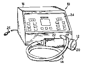
In Figure 1, a therapeutic ultrasound device is shown
generally at 10 for the medical application of ultrasound
energy to a patient. The device 10 ;ncludes a hand-held
- transducer 12 connected by a cable 14 to a base unit 16. The
cable 14 is re~ovably connected to the base unit 16 by a
connector plug 18 so that replacement of the transducer 12 ;s
possible. The transducer 12 has an ultrasound energy
emitting face 20 disposed at an angle to a handle portion 22,
~hich is gripped by the therapist or operator. A front
control panel 24 is provided at an angle for easy access by
, the operator and includes a plurality of display and control
means ~or controlling the transmission of ultrasound energy
from the transducer 12. A power cord 26 is also provided for
the base unit 16 by which the device 10 is connected to a
standard electrical outlet.
With reference to Figure 2, one embodiment of a
control panel 24 is shown therein, including a treatment time
display 28 and treatment time controls 30 by wh;ch the
desired number of minutes for treatment is selected.
Individual selection buttons or switches 32 are included in
the treatment time control 30 for selection of the more
popular time settings. Fine up and down adjustment switches
34 are also included for selecting time intervals not
represented by an individual switch 32. The treatment time
-4-
.
1324817
display 28 is preferably a numeric display, such as seven
segment numeric LED or LCD displays.
The display panel 24 also includes an output
intensity display 36, also preferably a numer;c display,
which displays the ultrasound enerqy output in watts per
sguare centimeter. An output intensity control 38 has
individual selection switches 40 for setting predetermined
intensity values as well as fine adjust switches 42 for
selecting other intensity values.
A duty cycle control 44 enables an operator to select
either a continuous output waveform or a pulsed output
waveform of various duty cycles. In the illustrated
embodiment~ an operator may select a continuous duty cycle by
depressing switch 46 or may select one of three pulsed duty
cycles of 25%, 50%, or 75% by operating a corresponding one
of the switches 48.
By selecting a treatment time, an output intensity,
and a duty cycle, after power up of course, the unit begins
operating to transm;t ultrasound energy from the transducer
12. The present invention senses the amount of the suppl;ed
power which is actually transmitted to the patient and
displays the transmitted, or coupled, power as a percentage
- or fraction of the maximum available ultrasound power by a
coupling indicator 50. The coupling indicator 50, in the
preferred embodiment, is a light bar which indicates coupl;ng
efficiency from 0% to 100% so that the operator gets a visual
clue of the amount of ultrasound power actually being
received by the patient. The operator can thereby quickly
determine if the transducer 12 is properly applied and
thereafter make adjustments. The light bar coupling display
1324817
50 of one embodiment includes 16 LEDs 52 connected to form
the individual illuminated segments of the bar graph 50.
Additional controls and displays on the front panel
24 include an output on indicator 54 to show when ultrasound
energy is being delivered to the transducer 12 and an error
indicator 56 to indicate a machine fault, such as a short
circuit or a broken cable, resulting in the unit lC being
automatically shut down. A display power watts switch 58 is
x operable to change the output intensity display 36 to a
10 display of total output power in watts. When the display
watts switch 58 ;s released, the display 36 reverts back to a
display of intensity in watts per square centimeter. Another
switch is the test switch 6~ which is manipulated to initiate
a self-test of the microprocessor memory circuits and the
displays on the front panel 24 of the unit 10, the results
thereof bein~ displayed by an OK indicator 62. By
maintaining the test switch 60 in a depressed condition, a
transducer tuninq control can be adjusted until properly
tuned as indicated by the coupling indicator 50. A reset
control 62 is also provided by which the control circuitry
- can be placed in a known state. The control switches on the
front panel 24 are preferably formed by touch pad switches,
althou~h other control means may also be used. Likewise, the
displays may instead be other display means.
In Figure 3, a functional block diagram of the
control circuitry for the ultrasound therapy device 10
includes a microprocessor 70 linked by a non-multiplexed
address, data, and control bus 72 to a variety of periphera~
and control devices. The microprocessor 70 of a preferred
embodiment is a four MHz. eight bit ~80 microprocessor. The
-6-
1324817
microprocessor operates under the control of a program stored
in an 8 K by 8 bit PROM 74, and utilizes a 2 K by 8 bit RAM
unit 76 for storage of information and variables as needed.
The program, among other things, enables the microprocessor
70 to provide servoing of the ultrasound output. A keyboard
78 and a display 80 provide a communication link between the
user and the microprocessor 70 through a dual eight-bit
parallel input/output port ~I/O) 82. The keyboard display
blocks 78 and 80 are the e~uivalent of the front panel 24
controls and displays.
-` The microprocessor 70 switches an ultrasound power
; amplifier 84 on and off throuqh a four-channel counter~timer
circuit (CTC) 86. An SCR power supply 88 supplies the high
voltage for the power amplifier 84. The SCR power supply 88
~ 15 is controlled by a trigger pulse from the counter timer
- circuit 86. An eight channel analog-to-digital tA~D)
converter 90 monitors the device parameters, i.e. amplifier
voltage, current, phase, and status, for transmittal to the
microprocessor 70.
Other functional blocks shown for the control circuit
include an address decoder 92 by which the microprocessor 70
accesses information in the memories 74 and 76, as well as
information transmitted and received through the I/O port 82,
by select lines from the decoder 92 to the other circuits.
The address decoder 92 is connected to operate a sound
` generator 94 which feeds an audio output 96, such as a
speaker, to alert the operator to changes in the unit's
functions. A power-on reset block 98 provides a means for
not only switching the unit 10 on, but also for automatically
,
, ,. ~
-- 1 3248 1 7
placing the circuit in a known state by transmitting a common
reset signal.
The AC power signal is received at the AC input 26
and fed not only to the SCR power supply 88, but also to a
5 low voltage power supply 100, which in turn supplies power to
the balance of the control circuitry. A zero crossing
detector 102 likewise receives the AC power siqnal and
outputs pulses corresponding to the zero axis crossings of
the sinusoidal input. The pulses from the zero crossinq
detector 102 are transmitted to the four channel counter
timer circuit a6 that then initiates a delay before a trigger
signal is sent to the SCR power supply 88. By varying the
~elay between the zero axis crossing and the triggering of
the SCR power supply 88, tbe amplitude of the AC signal at
which the SCR 88 is triggered changes~ This enables the
amplitude of the SCR output to be varied. The switching
- amplifier 84, which is driven by the SCR power supply 88,
transmits its ultrasonic signal through a one MHz. filter 104
- to the transducer 12. The amplitude of the amplifier signal
varies as tbe SCR signal varies. The filtered one MHz.
signal at the transducer is monitored by a phase detector 106
which feeds a phase signal to the A/D converter 90 for use by
the microprocessor 70 in feedback or servo control of the
ultrasound output. Through software utilized in the
microprocessor 70, the phase signal in conjunction with a
voltage or current signal from the power amplifier power
supply is used for servo control of either the preset output
~ power or the output intensity.
In Figure 4a, the circuit is shown in more detail,
including the processor or CPU 70 connected to the PROM 74,
-8-
~2~317
the RAM 76, and the address decoder 92 by the bus 72. The
CPu 70 is, as stated above, a Z80 processor, and the PROM 74
~; is, for example, a 2764 dual in-line chip, the RAM 70 may be
a TMM2016 P/D and the address decoder 92 an LS138 chip. A
timer chip 120, for example, a 555 chip, i5 connected to
provide a reset signal to the CPU 70 at an input 122, as well
as to supply a reset signal to the bus 72. A bus frequency
~`~ generator 124 includes an oscillator 126 connected to a clock
input 128 of a high speed timer 130 whicb ~eeds two J-K
flipflops 132 and 134 to generate a high speed bus
frequency. The bus frequer.cy in a preferred embodiment is
twice the ultrasound frequency of the transducer 12, i.e. for
a 1 MHz. ultrasound output, a 2 MHz. bus frequency is used.
If an optional 3 MR2. trans~ucer is used, a 6 MHz. bus
frequency is used. The high speed timer 130 of one
embodiment is an LS166A chip.
In Figure 4b, the A/D converter 90 is, for example, a
chip AD7581R~, while the two I/O ports 82 are shown as Z80
PI0 integrated circuits 136 and 138. The A/D converter 90 is
connected to a voltage reference element 140, which, for
example, is an A6585J. Note that analog ground 142 is
distinguished from digital ground 144 and the two are only
`f connected at the A/D converter 90. A sound generator 94 is
formed by a J-R flipflop 146 connected to a Darlington pair
148 which feeds a speaker 150. The sound generator 94
enables the microprocessor 70 to produce audio signals of any
audible frequency. Each time the circuit is "addressed~ over
a sound lead lS2 by the microprocessor 70, the flipflop 146
changes state and, since the flipflop 136 is capacitively
1 30 coupled to drive the speaker 150, a momentary pulse of
.
_9_
~, . '
--` 1324817
current is generated through the speaker 150 each time the
flipflop 146 changes to a high logic state to cause the
speaker cone to deflect and emit an audible click. For
example, addressing the speaker 150 two thousand times per
second produces an audible frequency of one RHz.
In Figure 5, various pin interconnects for the
control circuitry are shown, as well as a data buffer 154 and
address buffers 156 and 158. A switching circuit 160, for
example, an ALS53~, is also included.
The power supply for the unit 10 is shown in Figure
6, including the AC connector 26 and a double-pole single-
throw power switch 166 connected by a fuse 168. A filter 170
is provided between the switch 166 and a main power
transformer 172 that includes three secondary windings 174,
176, and 178. For added safety, a thermal cut-off 180 is
mounted internally of the transformer 172. The first
secondary winding 174 is connected to an input 182 of the
sero crossing detector 102 which is formed by, among other
thing;s, an 8T20 integrated circuit chip. The zero crossing
detector 102 is a bi-directional one shot which emits a pulse
from an output 184 at each zero axis crossing of the 60 Hz.
power signal. Thus, the output at lead 184 is a 120 ~z.
signal that is used for microprocessor program timing
functions and which is sent to the counter timer circuit
86. The secondary winding 174, which in a preferred
embodiment is a 15.7 volt RMS center tapped winding, is fed
~hrough diodes 186 and a filter arrangement 188 to a 5 volt
integrated circuit regulator 190. The 5 volt regulator 190,
which is, for example, an LM223AR, supplies a 5 volt DC
--10--
~ 1324817
signal between the 5 volt DC supply lead 192 and the digital
ground 144.
The second secondary winding 176 of the main
transformer 172, which is preferably a 31.8 volt RMS center
tap winding, is fed through a full wave rectifier 194 and
filtering elements 196 prior to being regulated by a pair of
symmetrically connected l; volt regulators 198 and 200. The
voltage regulators 198 and 200 produce a +15 volt signal and
a -15 volt signal, respectively, at the leads 202 and 204,
between which is connected the analog ground 146. The
voltage regulators 198 and 200 can be 78M15 and 79Ml~
integrated circuits, respectively.
The third secondary winding 178 of the main
transformer 17~ forms part of the SCR power supply 88 that
supplies DC current to the ultrasound amplifier 84 whicb is
used to produce the one MHz. ultrasound output signal. The
winding 178 is preferably a 130 volt RMS center tapped
winding and, since it forms part of the radio frequency
` portion of the circuit, it is shielded from the other
secondary windings 174 and 176 by a shield 206. This is in
addition to the usual Faraday shield 208 between the primary
- and secondary windings. A full wave rectifier 210 connects
the secondary 178 to the anode of a silicon controlled
rectifier (SCR) 212. The SCR 212 is normally in the off-
state and no current flows through it to a filter capacitor
214. The SCR 212 is triggered by a signal from the counter
timer circuit 86 through a transformer 216 and produces an
output on lead 217.
In operation, each time the AC signal crosses the
zero axis, the zero crossing detector 102 sends a pulse to
.
- 1324817
the counter timer circuit 86. The counter timer circuit
initiates a timing period wh;ch is established by the
processors 70 and is ~ased on the output intensity selected
by the operator. The timing period of one embodiment ranges
from 8.3 milliseconds to 4.1~ milliseconds. The longer time
period allows the entire AC half-wave to pass before the SCR
212 is fired and, thus, no energy passes through the SCR 212
to the filter capacitor 214. The shortest time period
triggers the SCR 212 exactly when the half-wave is at its
peak voltage. This produces the highest possible voltage on
the filter capacitor 214. The capacitor 214 is large enough
to store the energy needed by the ultrasound amplifier 84
through many cycles. Thus, the energy being pulsed into the
filter capacitor 214 at a rate of 120 times per second is
smoothed into a constant voltage and fed to the ultrasound
amplifier 84.
The ultrasound switching amplifier 84, which actually
produces tbe ultrasound signal for transmission to the
transducer 12, is shown in Figure 7. Included is an 20 oscillator portion 218, which is shown as a Colpitts
oscillato~ having an FFT 220. In place of a separate
oscillator 218, the bus frequency signal may be used for the
amplifier 84. The use of the processor ci~cuit's timing
signal as the frequency generator for the transducer 12
avoids the necessity of tuning the transducer 12 to the
control circuit. The oscillator output, or alternately the
bus frequency, is fed to a preamplifier 222 having an
operational amplifier 224 and a pair of NAND logic gates 226
and 228.
-12-
1 3248 1 7
A power amplifier portion 230 includes a transformer
232 with a center tapped secondary connected to a pair of
high speed FETs 234 and 236. The FETS 234 and 236 are shown
herein as insulated gate field effect transistors ~IGFET).
The two FETS 234 and 236 are alternately switched to
saturation and to off, one FBT being in a saturated state
when the other FE~ is off. The resultant signal is a nearly
square wave output. The power amplifier 230 is supplied with
power through the lead 217 from the SCR 212 so that as the
voltage on the lead 217 cbanqes the amplitude of ultrasound
output is changed.
An output f;lter 238 is connected through a
transformer 240 to the output of the power amplif;er 210.
The filter 238 is a two-stage filter which minimizes
freguencies other than the desired one MH2. output
frequency. Between the filter 238 and the transducer 12 is a
; power-factor correcting capacitor 242 that cancels the
~ .
inductive component of the load and enables the transducer 12
to operate at a frequency midway between series resonance and
parallel resonance for cooler and more efficient operation.
The addition of the capacitor 242 also matches the impedance
of the transducer 12 to the connecting cable to prevent
standing waves and reduce noise.
Since the high speed FETs 234 and 23~ are operated at
either saturation or off, the operation of the switching
amplifier 230 is very efficient. Little power is used by the
amplifier 230 so that minimal heat sink devices are required
and no fan is needed whatsoever. Very nearly all the power
is supplied to the transducer crystal }2. In one embodiment,
up to 20 watts of ultrasound energy is produced at the
transducer 12.
-13-
1324817
The applied voltage lead 217 is sampled and sent to
the A/D converter 90 for transmittal to the CPU 70. The
current through the FETs 234 and 236 is likewise sampled on
lead 244 for mon;toring by the CPU 70. A comparitor 246
establishes a threshold level for the current and transmits
an over current signal on lead 248 when the threshold is
breached. ~pon the ovPr current condition being sensed, the
unit 10 automatically shuts down.
Also in Figure 7, the phase detector 106 includes a
pair of small toroid transformers 250 and 252 connected to
sample the voltage and current, respectively, at the
transducer load 12, while maintaining the transducer circuit
in direct isolation. The voltage transformer 250 has a
primary across the output of the filter 238 and the current
transEormer 252 has its primary winding in series with the
output of the filter 238. The secondary windings of the
transformers 250 and 252 are connected to comparison circuits
254 and 256, respectively, which convert the voltage and
current sine waves to square waves of equal amplitude while
~aintaining their respective phase relationship. An
exclusive OR logic gate 2S8 produces either a logic zero when
the signals are instantaneously in phase, or a logic l when
the signals are instantaneously out of phase. An operational
amplifier 260 filters and integrates the output from the
exclusive OR gate 258 to produce a voltage which reflects the
relative phase difference between the voltage and current.
~his phase voltage is transmitted to the A/D converter 90
over lead 262 for use by the processor 7Q, from which, among
other things, the degree of transducer/patient coupling is
determined. If the processor through software senses that
coupling has remained below a predetermined level for a set
-14-
1324817
~ time, such as two seconds, the output power level is
significantly reduced to prevent heating of the transducer
12.
Alternately, servoing can be accomplished by sensing
the square of the power amplifier power supply voltage, or
current, which is directly proportional to the ultrasound
output acoustic power. Servoing here is also accomplished by
software control of the processor.
In Fiqure 8, the counter timer circuit 86 is
controlled by the processor 70 to initiate a timing period
upon each zero cross;ng pulse from the zero crossing detector
102. The time delay pulse is transmitted on lead 264 to a
flipflop 266, which generates a trigger signal for the SCR
180 on lead 268 connected to ~he transformer 216. Two D
flipflops 272, 2~6, and a J-K flipflop 274 are connected in
series to generate on and off signals on the leads 278 and
280, respectively. A plurality of calibration switches 282
are operable to selectively ground data leads connected to a
bank of pull-up resistors 2B4, which is connected to the CPU
70 through data buffers 286. A high speed timer 2a8 receives
the bus frequency signal at a clock input 290 to strengthen
the signal for transmittal through a J-X flipflop 292 and
jumpers 294 and 296 to the balance of the control circuit.
~igures 9a and 9b show the front panel cirauitry,
including a 34 pin header 298 for connection to the I/O ports
136 and 138. ~he reset switch 64 enables the operator to
selectively place the circuitry in a known state.
A 3 x 6 matrix keypad 300 of SPST switches includes
the rest of the front panel control switches 32, 34, 40, 42,
46, 48, 58, and 60. The switches are debounced and decoded
-15-
.
1324817
by the microprocessor program. The I/O ports 136 and 138
provide an interface between the switches and the processor-
- 70, the six columns being driven by the port 136 and the
three rows being read by the port 138. Reading the keyboard
300 requires a series of program steps. First, the processor
70 writes a logic one to all columns and reads back the rows
to see if any keys or switches are operated. If one is
- detected, the program waits a few milliseconds for the switch
to stop bouncing and tries again. If a switch is still
closed, the program enters a subroutine to determine by row
and column which switch is pressed.
An LED driver 302 is also in Figure 9a for driving
the displays shown in Figure 9b. The driver 302 preferably
is an ICM 7218ClJl.
In Figure 9b, six digit display elements correspond
to the numeric displays 28 and 36 on the front panel 24 and
are connected to the driver 302. A plurality of LEDs are
also shown driven by latches 304, 306, and 308. The LEDs 52
form the coupling bar graph 50. Resistors 310 are connected
to the LEDs 52.
A current boosting element 312, such as a 74LS244
integrated circuit, is connected between the latch 304 and
the rest of the LBDs, which include resistors 314 and
correspond to the output on display 54, the error display 56,
the O~ display 62, the continuous output display 46, and the
pulse output displays 48. The displays are interfaced to the
microprocessor 70 through the I/O ports 136 and 138 by
transmitting the digit or LED information to the display by
the port 136 and strobinq the appropriate circuit through the
other port 138.
-16-
1324817
Thus, there has been shown and described a
therapeutic ultrasound device which provides a switching
amplifier for generating an ultrasound signal, the amplifier
being highly efficient and dissipating very little power in
the form of heat. The present device also includes a phase
detector which guantifies ~he phase relationship between the
voltage and current at the transducer 12; Tbe ultrasound
transducer dynamically changes its impedance depending on the
degree of coupling it makes with the patient's tissue. The
changing impedance is easily determined from the
instantaneous phase angle between the transducer voltage and
the transducer current. The phase detector provides phase
information to the processor 70 which, in addition to a
voltage or current signal, enables the processor through
software control to drive a visual coupling indicator, change
output levels in response to varying ~issue loads, and
reduces output power to incidental levels when gross
uncoupling occurs.
Alternately, the power amplifier supply current or
voltage are used for servo control through the software in
the microprocessor.
Anothe~ feature of the present invention is the
~ coupling bar display 50 which shows the degree of coupling
between the transducer and the patient for immediate
correction by the therapist.
- Although other modifications and changes may be
suggested by those skilled in the art, it is the intention of
the inventors to embody within the patent warranted hereon
all changes and modifications as reasonably and properly come
within the scope of their contribution to the art.
.
-17-