Note: Descriptions are shown in the official language in which they were submitted.
1 325267
This application is a division of Application Serial
No. 515,897, filed August 13, 1986.
BACRGROU~D OF THE I~ENTION
Field of the Invention
The present inventiorl relates to an apparatus for
generating an image from a digital video input signal.
The apparatus is improved so as to reproduce an image with
high quality.
Description of the Prior Art
In the past, methods generally referred to as the dither
j method and the density pattern method have been proposed
: for reproducing images of half tones. These known
methods, however, cannot provide satisfactory gradation of
dot size when the size o~f the threshold dot matrix is
small and, therefore, require the use of a threshold
matrix having a larger size. This is turn reduces the
resolution and undesirably allows tne texture of the image
to appear too distinctive due to the periodic structure of
the matrix. Therefore, deterioration of the quality o~
; 20 the output image results.
,. ~b
:,- - , . .. .
: , , . .. , . ~ ..
, :
. ~
1 325267
-- 2
In order to mitigate the above described problems, it has
been proposed to modify the dither method so as to allow
finer control of the dot size by the use of a plurality of
dither matrices. This metnod, however, requires a
complicated circuit arrangement for obtaining syncnronism
of operation ~etween the dither matrices so that the
system as a whole is large in size, complicated in
construction, and slow. Thus, there is a practical limit
in the incremental increase of dot size and the resultant
increment of density available by the use of a plurality
of dither matrices. In U.S. Patent No. 3,916,096, a
method of improving the conventional screening process is
described. As set fortn in this U.S. Patent No.
3,916,096, at column 8, lines 19 through 31:
The conventional screening process when
applied to a scanned image can be regarded
as a form of pulse-widt~)-modulation whereDy
a line of length X is laid down and repeated
at intervals of Y. The percentage
transmission (or reflection) of the
reproduced image is then Y - X/Y [sic.
should read (Y-X)/Y]. To be a linear
process (Y - X) must be directly
proportional to the amplitude of the scanned
video signal where the signal amplitude
represents the percentaye optical
transmission of the recorded original
image. A way of achieving this is by
comparing the amplitude of the video signal
with a sawtooth wave form and laying a line
forming a portion of a dot whenever the
sawtooth is larger than the video signal.
i See also U.S. Patent No. 4,040,094, which relates to
~, similar suoject matter.
~ .
,.
~ .. . . . .
' ' ; . -
'' .
. - ~ -
. .
1 325267
-- 3
However, even if the method described in this patent is
used in an apparatus for reproduction of an image, the
precision of gradation reproduction deteriorates due to
tne delay of response of the apparatus.
The conventional method described in U.S. Patent No.
3,91~ 6, produces a linear mapping from the analog video
signal to the pulse-width-modulated signal. As is known
in the art of printing, this linear mapping doés not
produce acceptable results because of the non-linear
distortions introduced in the nalf-tone printing process,
in particular when used with a laser beam print engine.
Therefore, to obtain high quality half-tone printing, a
method of non-linear mapping must be found. And, the
method di~closed in the noted U.S. Patent, as quoted
above, uses a complex arrangement to allow the use of
different sawtooth waveforms on successive scans.
SUMMARY OF THE INVEN~ION
Accordingly, an object of the pre~ent invention is to
provide an image processing apparatu~ for generating an
image from a digital video signal, that can overcome the
problems of the prlor art described above.
Anotner object of the present invention is to provide an
image processing apparatus, for generating an image from a
digital video signal, that permits reproduction of images
with high ~uality.
Still another object of the present invention is to
provide an image processing apparatus, for generating an
image from a digital video signal, that can provide, with
a very simple arrangement, a superior quality half-tone
image.
'
~; .
1 325267
-- 4
Another object of the present invention is to provide an
imaye processing apparatus, for geslerating an image from a
digital video signal, that permits reproduction of images
with high ~uality at high speed,
A furtber object of the present invention is to provide an
image processing apparatus, for generating an image from a
digital video signal, that can reproduce tone information
with a high gradation and without impairing resolution.
Still another object of tne present invention is to
provide an image processing apparatus that can correct the
tonal properties of the video image by providing a
non-linear mapping of the video signal onto a pulse-width-
modulated signal with a very flexible arrangement,
In accordance with a preferred emDodiment, the image
processing apparatus of the present invention processes a
digltal image input signal and includes a raster scanning
print engine for generating a series of successive
~canning lines. ~ pulse-widtn-moaulated signal generator
generates a pulse-width-modulated signal from a digital
image input signal input to the apparatus. A circuit then
applies the pulse-width-modulated signal to the print
engine to cause it to generate each line as a succession
of line segments. Tne lengths of the line segments are
controlled to produce a variaDle density line screen from
the line segments with the line screen comprising a
plurality of columns of the line segments.
In accordance with another aspect of a preferred
em~odiment of the present invention, the image processing
apparatus includes a pattern signal generator for
generating a pattern signal of predetermined period. A
pulse- widtn-modulated signal generator then generates a
pulse-width-modulated signal in accordarlce with the video
.' .
,' ' ' ' ~ ' ': , . , : : . ,
'. . ' :. ''
" " ~ ' '''
.~ , .
1 325267
-- 5 --
signal and the pattern signal that can be utilized by a
raster scanning print ensine or image forming device to
form an image.
More specifically, the print engine scans lines on a
recording medium with a beam in accordance with the
pulse-width-modUlated signal, and a synchronizing signal
generator generates a synchronizing signal for each line
scanned on the recording medium. The pattern signal
generator generates the pattern signal of predetermined
period in accordance with the synchronizing signal.
In accordance with still another aspect of the invention,
the digital input signal has a characteri~tic, and a
characteristic converting device converts the
cnaracteristic in ~rder to produce a converted digital
video signal. This signal is converted to an analog video
signal Dy a digital to analog converter. A
pulse-width-modulated signal is thereafter generated from
tni--- analog video signal and the pattern signal.
Other aspects, features, and advantages of the present
invention will Decome apparent from the following detailed
description of the preferred embodiments taken in
conjunction witn the accompanying drawing, as well as from
the concluding claims.
BRIEF DESCRIPTION OF THE DRA~JING
Fig. l is a simplified schematic illustration of a
preferred embodiment of the apparatus for generating an
image from a digital video signal in accordance with the
present invention;
Fig. 2 shows waveform-~ of ~ignal obtained at different
portions of the apparatus for generating an image from a
,
.
'
. .
,,," ~ , :
.. .. .
.
1 325267
-- 6 --
digital video signal shown in Fig. l.
Fig. 3 shows how Figs. 3A and 3B are assembled together to
illustrate details of the embodiment of the apparatus for
generating an image from a digital video signal shown in
Fig. l;
Fig. 4 is a scheMatic illustration of an optical scanning
system in a laser Deam printer to which the invention is
applicable;
Fig. 5 shows waveforms of signals o~tained at different
portions of the circuit shown in Figs. 3A and 3B;
Fig. 6 is an illustration of triangular wave signals
formed in the circuit shown in Figs. 3A and 3B;
Figs. 7(a) to 7(c) are illustrations of how triangular
wave signals may be adjusted in the embodiment of the
invention;
Fig. B is an illustration of a look-up table of a gamma
converting ROI~ 12;
Fig. 9 is a diagram showing the relationship between input
video signals and converted video signals;
Figs. lO(a) and lO(b) illustrate the relationship between
the scanning lines and the conversion table as used;
Fig. ll is a circuit diagram of a circuit for causing
phase shift of triangular wave signals between lines;
Fig. 12 is an illustration of trianyular wave signals
appearing in respective lines at different phases; and
.. . .
':, ' ' ' ' '. : ''
~: , ' ' '. .
. -:. - , ; -
,; ' ' :.
1 325267
Fig. 13 is an illustration of another embodiment of the
invention.
DESCRIPTIOl~ OF THE PREF~RED EMBODIMENTS
A preferred emDodlment of the invent ~ will De described
in detail herein with reference to the accompanying
drawing.
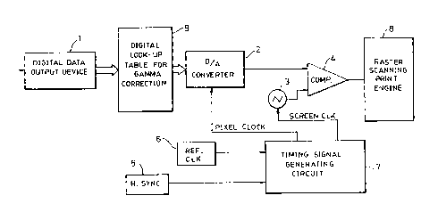
Referring first to Fig. 1 schematically showing an
embodiment of the invention, a digital data output device
1 is adapted to receive an analog video data from a CCD
sensor or a video camera (neither of whicn is shown) and
to perform an A/D (analog-to-digital) conversion of the
analog video signal so as to convert that signal into a
digital video signal, where each picture element (pixel)
is represented by a predetermined number of bits carrying
tone information. The digital video signal may be
temporarily stored in a memory or, alternatively, may be
supplied from an external device b~, for example,
telecommunication. The signal from the digital data
output device 1 is used as the address for a digital
look-up table for gamma correction 9. The resultant
output, which in tne preferred embodiment is an eight (8)
bit digital number ranging from OOH to FFH reprèsenting
256 possiDle tonal gradation levels as described further
below, is converted back into an analog signal by means of
a DtA (digital to analog) converter 2 so as to form an
analog signal which is updated for each picture element.
The analog video signal representing the picture elements
is fed to one of the input terminals of a comparator
circuit 4. simultaneouSly, analoy reference pattern
signals having a triangular waveform are produced by a
pattern signal generator 3 at a period corresponding to
the desired pitch of the half-tone screen. The pattern
.
,:: : - - ,,
- .
1 325267
-- 8
signals (a triangle wave) are fed to the other input
terminal of the comparator circuit 4. Meanwhile a
horizontal synchronizing signal generating circuit 5
generates horizontal synchronizing signals for respective
lines, while an oscillator lreference clock generating
circuit) 6 generates reference clocks. In synchronism
with the horizontal synchronizing signal, a timing signal
generating circuit 7 counts down the reference clocks, to,
for example, l/4 period. The signal derived fro~ the
timing signal generating circuit 7 is used as the clock
for the transfer of the digital video signal and also as
the latcn timing signal for the D/A converter 2.
In the embodiment described, since the apparatus is
intended for use in a laser beam printer, the horizontal
synchronizing signal corresponds to a beam detect (BD)
signal which is known per se. The comparator circuit 4
compares the level ol the analog video signal with the
level of the pattern signal of triangular waveform and
produces a pulse-width-modulated signal. The
pulse-width-modulatea signal is supplied to, for example,
the laser modulator circuit of a raster scanning print
engine 8 for modulating the laser beam. As a result, the
laser beam is turned on and off in accordance with the
pulse width thereoy forming a half-tone image on the
recording medium of the raster scanning print engine 8.
Fig. 2 shows the waveforms of signals obtained in certain
components of the apparatus shown in Fig. l. More
specifically, the portion (a) of Fig. 2 diagrammatically
shows the reference clocks generated by the oscillator 6,
while the portion tb) shows the horizontal synchronizing
signal mentioned above. The portion (c) shows the pixel
clocKs which are produced by counting down the reference
clocks with the timing signal generating circuit 7. More
specifically, the pixel clock shown in the portion (c) of
,~ ~ ' .
.,
,
1 325267
g
Fig. 2 is the signal which is obtained by counting down
the reference clocks into 1/4 period by the operation of
the timing signal generating circuit 7 in synchronism with
the norizontal synchrollizing signal. The pixel clock thus
obtained is delivered to the D/A converter 2 to be used as
the digital video signal transfer clock. The portion (d)
of Fig. 2 shows the pattern signal synchronizing clock
(screen clock) which is obtained by counting down the
reference clock into 1/12 period by operation of the
timing signal generating circuit 7 in synchronism with the
horizontal syncnronizing signal. In the illustrated case,
one pattern signal synchroni2ing clock is generated for
every -three pixel clocks. ~he pattern signal
synchr-onizing or screen clock thus obtained is delivered
to the pattern signal generator 3 to be used as the
synchroni~ing signal in the generation of the pattern
signal. The portion (e) of Fig. 2 shows the digital video
signal which is output from the digital data output device
1. And the portion (f) shows the analog video signal
after the D/A conversion conducted by the D/A converter
2. It will be seen from the portions of Fig. 2 that
picture element data of analog level are produced in
synchronism with the pixel clocks. It will also be seen
that the density of image Decomes higher, i.e., approaches
blac~, as the level of the analog video signal rises.
As shown by a solid line curve in the portion (g) of Fig.
2, the output from the pattern generator 3 is obtained in
synchronism with the clocks shown in the portion (d) and
is input to the comparator circuit 4. The broken line
curve in the portion (9) of Fig. 2 shows the analog video
signal shown in the portion (f). This video signal is
comparea by the comparator circuit 4 with the pattern
signal of triangular waveform derived from the pattern
signa~ generator 3 so that the analog video signal is
converted into a pulse-width-modulated signal as shown in
the portion ~h) of Fig. 2.
''
l 325261
~ 10 --
The described embodiment of the invention permits a
substantially continuous or linear pulse modulation and,
hence, ensures a high gradation of the image output by
virtue of the fact that the digital video signal is
converted into an analog video signal which is then
compared with the triangular wave signal of a
predetermined period.
It is to be noted also that, in the described embodiment
of the invention, the pattern signal synchronizing clock
(screeil clock) for generation of the pattern signal, e.g.,
the triangular wave signal, is generated in synchronism
witn the ho~izolltal synchronizing signal by making use of
reference clocks having a frequency much higner than tnat
of the pattern signal synchronizing signal. Therefore,
the ~itter of the pattern signal derived from the pattern
signal generator ~, e.g., the offset of the pattern signal
from one scan line to the next, is reduced to less than
l/12 of the period of the pattern signal. This precision
is required to insure a high quality half-tone
reproduction in which the line screen is formed uniformly
and smoothly from one scan line to the next. Therefore,
the density information can be accurately pulse-width-
modulated by making use of this pattern signal which has a
small fluctuation, so that the image can be reproduced
with high quality.
Fig. 4 is a schematic perspective view of the optical
scanning system incorporated in the laser beam printer (a
raster scanning print engine) to which the present
invention is applied. The scanning system has a
semiconductor laser adapted to emit a laser beam moàula~ed
in accordance with the pulse-width-modulated signal
mentioned a~ove.
. . .
,,
.
. ~ - . . :
; ~ ~. ,.
.. , ~ .
.:
~ 3252b1
The optical laser beam modulated by the semiconductor
laser 21 is collimated by a collimator lens 20 asld is
optically deflected by a polygonal mirror ~applying means)
22 having a plurality of reflecting surfaces. The
deflected ~eam is focused to form an image on a
photosensitive drum 12 by an image forming lens 23
referred to an fe lens, so as to scan the drum 12. During
tne scanning by the beam, and when the beam reaches the
end of each scanning line, it is reflected by a mirror 24
and is directed to a Deam detector 25. ~he beam detection
(BD~ signal produced by tne beam detector 25 is used as
the norizontal syncnronizing signal as ~s ~nown. ~rhus, in
tne descriDed emDodiment, the horizontal synchronizing
slgnal is consti~u~ed Dy tne BD signal.
It will be seen that the BD signal is detected for each of
the lines of -~canning by the laser beam and is used as the
timing signal for the transmission of tne
pulse-width-modUlated signal to the semiconductor laser.
As used in the subject specification in description of the
preferred embodinlents and as used in the concluding
claims, the term ~line-segment~ means a dot which is
formed on a recording medium~ the length (size) of which
is variable in accordance with the width of the pulse
widtn in the supplied pulse-width-modulated signal.
The apparatus for generating an image from a digital video
signal ~f the invention will be descrioed more fully with
specific reference to Figs. 3A and 3B which show details
of the apparatus shown in Fig. 1.
As stated before, the preferred emDodiment described
herein makes use of the BD signal as the horizontal
synchronizing signal. The BD signal, however, is
~asically asynchronou~ witn the pixel clock and,
1 325267
- 12 -
therefore, would normally cause jitter in the horizontal
direction. In the described embodiment, therefore, jitter
is reduced to less than 1/4 of the width of a pixel, by
making use of an oscillator 100 tnat can produce reference
clocks ~72M-CLK) (72 megahertz clock) of a frequency which
is 4 times higner than that of the pixel clocks. A BD
synchronizing circuit 200 is used for this purpose. The
reference clock (72M-CL~) from the oscillator 100 is
supplied to D latches 201, 202, and 203 through a buffer
101, while the BD signal is input to the data terminal D
of the D latch 201 through a terminal 200a so as to be
syncnronized with tne reference clocks. In addition, the
BD signal is delayed by the D latches 202 and 203 by an
amount corresponaing to 2 (two) reference clock pulses.
The BD signal thus delayed is delivered to one of the
input terminals of a ~OR gate 103, while tne other input
terminal of the NGR gate 103 receives the inverted output
of the D latch 201. The output from the NOR gate 103 is
input to one of the input terminals of a NOR gate 104,
while the other input terminal of the NOR gate 104
receives the output of a flip-flop circuit 102.
~ith this arran~ement, the flip-flop circuit 102 produces
clocks (36M-CLK) (36 megahertz clockl which are obtained
by dividing the frequency of the reference clock by 2
(two). Thus, the output (36M-CLK) from the flip-flo?
circuit 102 is synchronous witn the BD signal to within
one period of the clock 72M-CLK.
The output of the D latch 203 is delayed by the D latches
204, 205, and 206 by an amount corresponding to 3 (three)
pulses of the output (36M-CLK) of the flip-flop circuit
102.
The inverted output from the D latch 201 and the output
from the D latch 206 are delivered to a NO~ gate 207, so
' :
'`.' , , .
1 325267
- 13 -
that an internal horizontal synchronizing signal
(BD-Pulse) is formed in synchronism (within one period)
with the reference clock.
Fig. 5 shows the timing of the signals obtained at various
portions of tne BD synchronizing circ~:it 200. More
specifically, A-l ShOws the BD signal, A-2 shows the
reference clock ~72M-CLK) produced by the oscillator 100,
and A-3 snows the inverted out~ut from the D latch 201,
obtained by synchronizing the BD signal with the reference
clock (72M-CLK). A-4 shows the output from the D latch
203, obtained by delaying the signal A-3 by an amount
corresponding to 2 ~ two) reference clock pulses. A-5
shows the clock (36M-CLK) output from the flip-flop
circuit 102, A-6 shows the output from the D latch 206,
obtained by delaying the signal A-4 by an amount
corresponding to 3 (three) pulses of the clocks (36M-CLK),
and A-7 shows the internal horizontal synchroniæing
(BD-pulse). It will be seen that the internal horizontal
synchronizing signal (BD-Pulse) rises in synchronism with
the rise of the first reference clock (72M-CLK) after the
rise of the BD signal, and is held at level ~1~ for a
period corresponding to 8 (eight) pulses of the reference
clock. This internal horizontal synchronizing signal
(BD-pulse) constitutes the reference for the horizontal
driving of the circuit of this em~odiment.
An explanation of the video signals will now be made again
with reference to Figs. 3A and 3B. The pixel clocks
~PIXEL-CLK) are formed by dividlng the frequency of the
signal (36M-CLK) by 2 (two) by means of the J-K flip-flop
circuit 105. A 6-bit digital video signal is latched in
the D latch 10 by the pixel clock (PIXEL-CLK), and the
output is delivered to a ROM 12 for gamma conversion. The
8-bit video signal produced through the conversion by the
ROM 12 is further converted into an analog signal by the
., , , :
1 325267
- 14 -
D/A converter 13 and is delivered to one of the input
terminals of the comparator 15 in order to be compared
with the triangular wave signal explained below. The
pulse~width-modulated signal obtained as a result of the
comparison is delivered to the laser driver of a raster
scanning print engine.
Still referring to Figs. 3A and 3B, reference numeral 300
designates a screen clock generating circuit which
generates the screen clock, i.e., the analog reference
pattern signal synchronizing clock, which is used as the
reference for the generation of the triangular wave
signal. A counter 301 is used as a frequency divider for
dividing the fre~uency of the signal (36M-CLK) output from
tAe flip-flop circuit 102. The counter 301 has input
terminals D, C, B, and A which are preset with
predetermined data by means of a switch 303. The ratio of
the frequency division i~ determined by the values set at
these input terminals D, C, B, and A. For instance, when
tne values ~ , and ~1~ are set in the terminal~
D, C, B, and A, respectively, tne frequency of the signal
~36M-CLK) is divided into 1/~.
Meanwhile, horizontal synchronization is attained by the
NOR gate 302 and tne tBD-pulse) signal. The frequency of
the divided signal is further divided into 1/2 by a J-K
flip-flop circuit 304, so that a screen clock having a
duty ratio of 50~ is formed. A triangular wave generating
circuit 500 generates triangular waves by using this
screen clock as the reference,
Fig. 6 shows waveforms or signals appearing at various
components of the screen clock generating circuit 300.
~It is noted, nowever, that the scales of Figs. 5 and 6
are different). More specifically, L-l shows the internal
synchronizing signal (BD-PULS~ -2 shows the signal
, . .
'
1 325267
(36M-CLK) and B-3 shows the screen clock (SCREEN CLK) as
obtained wnen values ~ 0~ are set in the
terminals D, C, B, A of the counter 301, respectively.
B-4 represents tne triangular wave signal as obtained when
the screen clock B-3 is used as the reference. On the
other hand, B-5 shows the screen clock (SCREEN CL~) as
obtained when values ~ 0~ are set in the
input terminals ~, C, B, A of the counter 301. B-6 shows
the triangular wave signal as obtained when the screen
clock (SCREEN CLK) shown in B-S is used as the reference
obtained. It will be seen that the period of the
triangular wave signal shown by ~-4 corresponds to 2 (two)
picture elements, while the period of the triangular wave
signal snown by B-6 corresponds to 4 (four) picture
elements. l~hus, the period of the triangular wave signal
can De varied as desired by appropriately setting the
switch 303. In the embodiment described, the period of
tne triangular wave is cnan~eable between a duration
corresponding to 1 (one) picture element and a duration
corresponding to 16 (sixteen) picture elements.
The triangular wave signal generating circuit 500 will now
be descriDed, again with reference to Figs. 3A and 3~.
The screen clock (SCREEN CLK) is received by the buffer
5Ul, and the triangular wave is generated by an integrator
comprising by a variable resistor 502 and a capacitor
503. The triangular wave signal is then delivered to one
of the input terminals of the comparator 15 through a
capacitor 504, a protective resistor 506, and a buffer
amplifier 507. The triangular wave signal generating
circuit 500 nas two variable resistors, namely, variable
resistor 502 for adjusting the amplitude of the triangular
wave signal, and a variable resistor 505 ror adjusting the
bias or ofrset of the triangular wave signal. The
a~justment of the amylitude and the offset of the
triangular wave signal by the variable resistors 502 and
.. 7
- 16 - 1 32 5 267
S05 is conducted in a manner which will be explained witn
reference to Figs. 7(a) to 7(c). In Fiy. 7(a), a
triangular wave signal Tri-l before adjustment is shown by
a solid line curve. By adjusting the variable resistor
502, the signal Tri-l is changed into an amplified
triangular wave signal Tri-2 shown by a broken line
curve. Then, the variable resistor S05 can be adjusted to
snift or adjust the offset of the wave so as to form a
triangular wave signal Tri-3 shown by a
one-dot-an~-one-dash line curve. It is thus possible to
obtain a triangular wave signal having the desired
amplitude and ofr~et.
As statea Defore, the triangular wave signal tAus formed
is compared by the comparator 15 with the output of the
D/A converter 1~, i.e., witn the analog vlaeo signal. The
relationship between the triangular wave signal and the
analog vlaeo signal is preferaDly sucn tnat the maximum
level of the triangular wave equals the level of the
output of the D~A cQnverter 13 as obtained wnen the input
to the converter 13 has the maximum level (FF~, where H
indicates a hexidecimal numDer), wnile the minimum value
of the triangular wave signal equals the level of the
output of the ~/A converter 13 as obtained when the input
to this converter has the minimum level (OOH). Since the
amplitude and the orfset of the triangular wave can be
controlled as desired, it is possible to obtain this
preferred condition without difficulty.
More particularly, according to the invention, the
amplituae and the offset of the trianyular wave signal are
adjusted in the following manner. In general, a laser
driver for emitting a laser ~eam has a certain delay time
in its operation. The delay time until the laser beam is
actually emitted is further increased due to the beam
emitting characteristics of the laser. Therefore, the
. . . .
.- , ;
-: , . '' :
~, : : : .
1 3252b7
- 17 -
laser does not start emitting the laser beam until the
width of the pulse input t~ the driver exceeds a
predetermined value. This means that, in the case where
tne input signal is a series of periodic pulses as in the
case of the described embodiment, the laser does not emit
a Deam unless the input signal pulse has a duty ratio
greater than a predetermined value. Conversely, when the
duty ratio o the pulse is increased beyond a certain
level, i.e., when the period of low level of the pulse is
shortened, tne laser tends to stay on, that is, the beam
is continuously emitted. For these reasons, if the
adjustment of the triangular wave signal is conducted in
the manner shown in Fig. 7(b), the gradation levels around
the minimum level (00~) and near the maximum level (FFH)
are omitted from the 256 gradation levels of the input
data which ~ay ~e input to tne D/A converter 13, so that
the gradation deteriorates undesirably. In the embodiment
described, therefore, the variable resistors 502 and 505
are adjusted so that the pulse width just below that which
will cause the laser to begin emission is obtained at the
OOH level of the data input to the D~A converter 13, and
80 that the pulse width which will render the laser
continuously on is obtained at tne FFH level of the data
input to the D/A converter 13. This manner of adjustment
of the variable resistors 502 and 505 is shown in Fig.
7~c).
As will be understood from Fig. 7(c), tnis preferred
embodiment is designed so that the comparator lS produces
an output pulse of a certain pulse widtll (a pulse width
just below that which will cause the laser to begin
emission) when the minimu~ input data OOH is supplied to
the D/A converter 13. '~he preferred embodiment is also
designed so tnat, when the maximum input data FFH is
supplied to the D/A converter 13, the comparator produces
output pulses the duty ratio of which is not 100% but
: . - :. . -
: - ,.~., : - :
1 325267
- 18 -
which is large enough to allow the laser to emit the beam
continuously. This arrangement permits the emission time
of the laser to vary nearly over the entire range of the
256 graaation levels of the input data, thus ensuring high
gradation of the reproduced image.
It snoulà ve under-~toaà that the method descriDed above is
not limited to a laser printer but may also be utilized in
to an inK jet printer, a thermal printer or other raster
scanning devices.
The ROM 12 for gamma conversion will now De explained in
detail with reference to Fig. 8. The ROM 12 is provided
to allow a ni~h gradation of density in the reproduced
image. Although the described embodiment employs a ROl'l
having a capacity of 256 bytes as ROM 12, a capacity of 64
bytes is basically enough because the input digital video
signal is a 6-bit signal. Fig. 8 shows the memory map of
the ROM 12 for gamma conversion. Since this ROM has a
capacity of 25~ bytes, it can contain 4 (four) separate
correction tables, namely TABLE-l including addresses UOi~
20 to 3FH, TABLE-2 including aadresses 4~ to 7FH, TABLE-3
including addresses 80H to BFH, and TABLE-4 including the
acaresses CO~ to FFH.
Fig. 9 shows a practical example of the input-output
characteristics of each of the conversion tables, i.e.,
the relationship between the input video signals and the
converted output video signal. As will be seen from tnis
Figure, the 64 (sixty-four) levels of the input video
signal are converted into levels O to 255 (OOH to FFH) in
accordance witn the respective conversion tables. The
change-over between the conversion tables can be made by
varying the signal applied to upper terminals A6 and A7 oE
the ROM 12 as shown in Fi9s. 3A and 3B. The descriDed
embodiment is designed to allow this switching for each
... .
-
... . ~ . . ;
.' . ,. -: .
'~ ' - '~: . -
1 325267
line, by the operation of a circuit 400 shown in Fig. 3A.
In operation, the internal norizontal synchronizing signal
~BD-Pulse) is input to a counter 4~1 the output of which
i~ delivere~ througn terminals Q~ and ~ to the terminals
A6 and A7 of the ROM 12. The counter 401, in cooperation
with an RCO inverter 402 and a switch 403 constitutes a
ring counter, so tnat the period of ~ ~-ching of the
conversion taDle can be varied in accordance witn the
state of the switch 403. For instance, when the switch
403 has the state ~1~ (at terminal B), ~1~ (at terminal
A), TABLE-4 is always selected, whereas, when the state of
tne switch 403 is ~1~ (at terminal B), ~0~ (at terminal
A), TABLE-4 and TABLE-3 are selected alternately. When
the swltch 403 has the state of ~U~ (at terminal B), ~0
(at terminal A), TABLE-l, TABLE-2, TABLE-3, and TABLc-4
are successively selected for successive lines, as shown
in Fig. 10a. Moreover, it is possible to improve the
gradation by cnangin5 tne conversion table for successive
lines.
In general, ln tile electropnotograpnic reproduction of an
image, the gradation is more difficult to obtain in the
light portion of the image than in the daek portion of the
image. Therefore, as in the example shown in Fig. 9, the
conversion taDles are substanti~lly duplicated in the dark
portions of the image and differ in the light po~tion so
as to provide optimal gradation.
In the preferred embodiment, the switching of the table
can also be made in the direction of the main scan by the
laser beam.
More specifically as shown in Figs. 3A and 3B, a signal
can be formed by dividing the frequency of the screen
clock (SCREEN-CL~) by 2 (two) by means of a J-K flip-flop
circuit 404, inputting the resulting signal to one input
.:
:: ' ,. , , - ,
r.
::'-' ': : -
: '' .` . : .'
i :-
'
1 325267
-- 2U --
terminal of an exclusive OR circuit 406, the other input
of whicn is connected to terminal QB of the counter 401
and the output terminal of which is then connected to ROM
12 tnrough a latch ll. With this arrangement, it is
possible to change the conversion table in a staggered
manner as shown in Fig. 10(b), thus attaining a further
improvement in the gradation. A reference numeral 405
denotes a switcil for selecting either switching of the
table in the staggered manner described above or not so
switching. The staggered switching of the table is
selected when this switch has the ~l~ level and is not
selected when the switch has the ~0~ level. The numerals
appearing in frames of the table snown in Fig. l0(b)
represent the numDers of the selected conversion ta~les l
to 4. Thus, the period of the screen clock in the
em~odiment corresponds to ~he period of 3 ltnree) pixel
clocks.
It will De understood from the description provided above
that the scanning lines produced by the laser in
accordance with data from the conversion tables of the ROM
12 are each generated as a succession of line segments.
The line segments of successive scanning lines
collectively form a plurality of columns that aefine a
line screen.
More particularly, when the video signal processed by the
circuit shown in Figs. 3A and 3B is directly delivered to
a reproducing means such as a laser beam printer, the
reproduced image has a structure with vertical columns (in
the described embodiment, the line screen is composed of
vertical columns of line segments of successive scanning
lines which form in the reproduced image) due to the fact
that the phase of the triangular wave signal is the same
as that of tne internal horizontal synci~ronizing signal
(BD-Pulse) for each line. l'he circuit in the present
. :
~ ~: , - .,
.. ~ . :
. .; -
.,! :
" :
1 325267
- 21 -
embodiment is one in which the triangular wave is formed
after the reference clocks are counted by 12 (twelve) from
the rise of the BD-Pulse signal. The timing for the
generation of triangular waves is the same for each line,
and so each phase of the triangular waves on each line is
the same. The image data is output from the digital data
output device 1 as stated above. The digital data output
device 1 outputs image data with a predetermined timing in
synchronism with a signal equivalent to the BD-Pulse
signal. More particularly, the data output device 1 is
adapted to receive the BD signal. This device 1 starts to
count tne reference cloc~ after receiving the BV signal,
and begins transmission of the image data after counting
tne rei~rence clocks up to a predetermined nur~ber. As a
conseyuence, the timing of transfer of the image data
necessary ror image reproduction is the same on each line,
and a high quality reproduced image with no image jitter
can be pro~uced. As the timlng of the generation of the
triangular waves and the timing of transfer of the image
data necessary for image reproduction have the same
relation on all of the lines, the reproduced image has its
vertical column structure with no image jitter, which is
effective, for example, in reducing a particular Moire
pattern. Again this vertical column structure comprises a
line screen having a vertical columnar axis extending at
an angle, that is perpendicular to the raster scanning
lines.
It is also possible to obtain a reproduced image having a
structure comprising oblique line screen columns, if the
phase of the triangular wave signals is made to be offset
slightly for successive lines. This is effective in
reduciny the l~oire pattern wnich appears undesirably when
an original dot image is read and processed. The angle of
inclination of tne obli~ue columns can be determined as
desired by suitably selecting the amount of shift of the
. .
.
: ~ : :
: . . . .
:- ,, - ,. ~ .: - .. -.. .
: . . :
; , ~ ~..... , , .:
1 325267
- 22 -
phase of the screen clocks for successive lines. For
instance, a reproduced image comprisiny scanning lines
having oblique columns inclined at 45 degrees can be
obtained by shifting tne triangular wave signal by an
amount corresponding to one picture element, i.e., by
phase snifting tne triangular wave signal 120 degrees for
each of the successive columns. Fig. 11 shows a circuit
for reproducillg an image comprising oblique columns. More
specifically, a reproduced image comprising oblique
columns can ~e oDtained by using tnis circuit in place or
tne screen clock generating circuit 300 in the circuit
sAown in Fig. -~.
Referring again to Fiy. 11, the internal horizontal
synchronizing signal (BD-Pulse) is latcned by the pixel
clocks (PIXEL-CLK) by means of D latches 356 and 3;7, so
that three internal horizontal synchronizing signals
(BD-Pulse) ilaving dirferent phases are produced. Then,
one of these three internal horizontal synchronizing
signais ~BD-~ulse) is selected for eacll line Dy operation
of a counter 35a, inverters 359 and 360, and gate circuits
361 to 367. The selected signal is input as a LOAD signal
to a counter 351, thereby changing the phase of the screen
clocks for successive lines- The counter 351 is adapted
to divide the frequency of the signal (36M-CLK) into 1/3,
while tne J-K ~lip-flop circuit 354 furtner divide~ the
frequency of the output from tne counter 351 into 1/2.
With tnis arrangement, it is possiDle to generate one
screen clock for every three picture elements.
Fig. 12 shows timing of the screen clock generated by the
circuit of Fig. 11 and the triangular wave signal for
successive lines. These three triangular wave signals are
generated in sequence of eacn set of each 3 lines.
,.,. - - - , -................ ~ .
. ~
-, . :., ' :
~- ~'' : -
, ~ - :,:
1 325267
- 23 -
~Ihen the reference pattern signal is generated in
syncilronism with a group of picture elements as in the
case of the embodiment described, it is possible to shift
the synchronizing signal used in tne generation of the
pattern signal by an amount corresponding to one half of
the reference pattern signal period for each successive
set of scan lines equal to the widtn of the pattern
signal. ~ucn a method allows the position of the center
of growth of the pulse width to be shifted in each of
successive lines, so that the output image can have an
appearance resemDling that produced by half-tone dots
arranged along oblique lines.
In the circuit shown in Figs. 3A and 3B, the RO.~I 12 is
u~ed for the purpose of gamma conversion. This, nowever,
is not tne only element suitable for this purpose and the
R~M 12 may De replacea Dy an S-~All connectea to tAe DATA
BUS line of a computer. ~1ith such an arrangement, it is
possi~le to rewrite the ga~na conversion ta~le as desired
in accordance w-th, for example, a change in the kind of
the original, tnus increasing the adaptaDility of the
apparatus of tne invent-on.
Fig. 13 snow~ an exam~le of a circuit which is usable in
place of the ROM 12 in the circuit shown in Figs. 3A anà
3B. This circuit llas, as will be seen from this Figure,
an S-RAI~ 12a for gamma conversion, a decoder 30, a
microcomputer 31 ror re~riting the gamma conversion
tables, tri-state buffers 32 and 33, and a bi-directional
tri-state buffer 34.
The mode changing switcnes 304, 403 and 405 in the circuit
shown in Figs. 3A and 3B may be controlled by the
microcomputer 31 so as to increase the flexiDility of the
system as a whole.
:`
: ..
.
,
. ..
.. . : -
1 325267
- 24 -
Although the invention has been described with reference
to specific emDodiments and in specific terlns it is to be
understood that this description is only illustrative
purposes ana that various other cnanges and modifications
are possible without departing from the scope of the
invention.
. . . : : .
. .
-` ' : ,, ,