Note: Descriptions are shown in the official language in which they were submitted.
3 2 ~7 30 21766-548
The present invention relates to a radiation transducing
device.
; Radiation transducing devices of the prior art, e.g.
EP-A-015714, consist of a matrix of pixel elements wherein each
pixel element is scanned sequentially, similar to the scanning of
pixel elements in a television or video apparatus.
The state of the prior art is further described in
EP-A-0260858 and in the article: "The VLSI design of a two dimen-
;~ sional image processing array" of D. Panogiotopoulos e.a., pub-
~' 10 lished in Microprocessing and Microprogramming, vol. 14, no. 3/4,
October/~ovember 1984.
When scanning a picture area in which only one or some
locations contain radiation to be detected, the transducing
devices of the prior art produce an enormous amount of signals the
.,.~ .
information content of which has substantially no value at all.
It is an object of the present invention to improve upon
.^,j
the prior art and to provide a new radiation transducing device.
~i The present invention provides a radiation transducing
~,
-i device for transducing radiation, comprising: an array of radia-
-~i 20 tion sensitive elements, comparator elements connected to at least
l a portion of said array for comparing the amount of radiation
received by the radiation sensitive elements to a predetermined
threshold value, encoding element connected to said comparator
elements for producing an output effective for identifying the
location of said radiation sensitive elements which have been
,
~exposed to radiation and measuring means connected to said
, ,~ , ,
:~ , , - ,
.
-'' ' ~ ~ .
32~73~
~ - la - 21766-548
. ,
radiation sensitive elements for determining the amount of
, incident radiation collected in an element during a predetermined
~' time period.
, The field of application of the present invention con-
~
cerns fast sequential recording of collisions of elementary parti-
cles in experiments at high energy storage rings, e.g. at CERN, as
' well as the continuous watching of ground environment, e.g.
J detection of flashes of lightning occurring above the ground.
.~
A preferred embodiment is provided with means for detec-
ting two or more so-called events separately.
Further advantages, features and details will be clari-
fied in view of a preferred embodiment of the radiation transdu-
cing device according to the present invention, described with
reference to a drawing, which shows:
fig, 1 a diagram of a preferred embodiment of a radia-
tion transducing device according to -the present invention;
'~ ''
,,:.j
. . .
3i
. `, "
",
~: i
"''
: ,~
.~
:~ : . .
'; ~, . '
:''`',- , :,- .
, ,: - :
,,',`:, - : ' " `'` :
` 132~73~ `
fig. 2 a diagram of an embodiment of a radiation
sensitive element of the diagram of fig~ 1;
fig. 3 a diayram of a comparator element of fig. l;
fig. 4 a diagram of the connection of the source
', 5 followers of fig. 2;
~ fig. 5 a diagram of an embodiment of the encoding
J elements of fig. 1;
~, fig. 6 a diagram of a second preferred embodiment
of a radiation transducing device according to the present
lO invention; and
fig. 7 a diagram of detail VII of fig. 6.
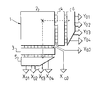
A preferred embodiment of a radiation transducing
device l (fig. l) comprises a matrix 2 of arrays of radiation
sensitive (pixel~ elements, in which both in lying (x) and
15 standing (y) direction a comparator element is connected to
;,~ each row of pixel elements which are connected in parallel to
.~
each other (similar as shown in fig. 4), as is diagrammatic-
; ally set forth by blocks 3, 4 resp... To comparator blocks 3,
4 resp. encoding blocks 5, 6 resp. are connected, of which
20 output xol, x02, x03, xo4, Yol, Yo2, Yo3, yo4 resp- are
~! derivable, as will clarified in the following description.
Outputs xaO, YaO resp. are directly derivable from the
outputs of the matrix or pixel elements.
~, A preferred embodiment of the pixel element 7
25 (fig. 2) of the matrix 2 comprises a radlation sensitive
element in the form of a photo sensitive diode 8 on which
radiation R is incident, which is connected through an
inverting amplifier 9 having FET's lO, 11 resp. for producing
a signal to comparator blocks 3, 4 resp. sald FET's connected
~i 30 as source followers. A capacitor 30 and a electronic reset
`i switch 31 are connected over the inverting amplifier 9.
~`` Outputs xaC and Yar produce (in a not shown way),
? similar to the way shown in fig. 4 for each column, row
` resp. an output signal xac, Yac resp., which form a common
~5 output signal for each column, row resp. of the matrix 2. For
the purpose of deriving such a common output signal the
source followers 10, 10', 10'' etc., the source follows ll,
~.~
,
,`~ : ~ ............................. . .
~ . .
~32~3~
, -3-
., .
11', 11'' etc. resp. of each pixel element are connected in
, parallel for each column, row resp
j A comparator element, e.g. a NOR-flipflop 12, is
connected to the output xac (and Yar) of each row (and
5 column) of the pixel matrix. A threshold value for switching
dependent on the amount of radiation incident on a
photosensitive diode 8 is determined by the dc bias level of
the input xac relative to the negative supply voltage. This
dc bias level can be set e.g. by means of the setting of the
10 inverting amplifiers 9. The input 15 of the NOR-flipflop 12
`~ forms a reset terminal, which may initialize a new image
~: recording. The output 16 has a logic ~'0" or ~ value,
i, dependent on the fact whether or not the amount of radiation
, incident to the corresponding column (or row) of the matrix
.~ 15 is higher than a predetermined (and preset) value.
The (analog) output xa0 (fig. 4) (~nd YaO in a
corresponding row) is formed, because of the fact that source
~! followers 32, 32', 32'' etc. are connected in parallel and in
series to a load or measuring element 21. When radlation is
20 incident to more than one row or column of the radiation
sensitive elements 8, the voltage over the load 21 is
determined by the largest amount of radiation incident to a
~hit~ element. The load 21 will in most cases be a resistor,
i but may also be a switchable capacitor.
, 25 The encoding block 5 and 6, preferably of similar
~; structure, may be realized by means of a multiplexer. In this
~, way a data reduction is achieved e.g. for a 100 x 100 image
`, transducing element of thus 10,000 pixel elements of e.g. 100
x 100 ym2 each, of 10,000 to 100 data for each image period.
30 The image period can decrease from 1 msec to 10 ~sec or the
energy consumation may decrease by a factor of 100 in a
corresponding way. Further the number of clocking member and
~` power supplies for controlling the image transducing element
of the present invention is limited relative to known CCD
35 transducing devices.
Preferably a combinational logic circuit is used as
coding block 5, 6 resp., of which an embodiment (of which
. .
.
;,
., .
. ;,
: ` :
" ~32~73~
--4--
''
purpose of simplicity only 8 bits are shown, is disclosed in
~' fig. 5; the image period can be reduced to e.g. 100 nsec by
means of this embodiment, or the energy consumption can be
, reduc~d to less than 1 mW. The circuit of fig. 5 comprises-, 5 NOR-circuits 21, invertors 22 and OR-gates 23. The circuit is
to be seen as built of base block A and B+ The shown
embodiment accomplishes the encoding for eight inputs ~Io-I7)
connected to outputs 16 of the comparator elements. By means
of block A and B a circuit for a number of inputs larger than
10 eight can be built in a simple way.
The outputs of the circuits shown in fig. 5 produce
1 in a consecutive way from the top down:
- Y/N: whether or not an amount of radiation above
a preset threshold value to the radiation transducin~ device
;~l
15 is present;
- Mss the most significant bit value of the row or
' column of the pixel element having the highest rank number of
l the pixel element to which radiation was incident;
i - 2SB the centre bit value of a row or column
20 having the highest rank number to which radiatlon was
..,
incident; and
- LSB the least significant blt value of a row or
, column having the highest rank number of the pixel element to
which radiation was incident.
When two encoding circuits of fig. 5, in the
preferred embodiment of the radiation transducing device
(both to x and y side) are dlsposed, while inputs Io-I7 are
; supplied in inversed sequence to a second encoding clrcuit,
- the following may be determined from a comparason of bit
30 values at the outputs, because one encoding circult detects
~- the lowest and the other the highest activated row (or
, column) value:
- the same result means that only pixelelements of
one row, column resp. are activated by radiation; or
- an unequal result defines the horders of an area
in which at least two rows (or columns) of pixelelements are
activated.
'
... .
,: ~
::
~: . . :- . : :. . . .. .. : .
~ ` 132573~
--5--
:
.
Preferably the output of the encoding blocks 5, 6
resp. contain the following information:
- x0l (Yol) a bit which defines whether or not a
pixel element in a column (row) is activated (Y/N of fig. 5);
- x02 (Yo2) a digital number defining the highest
column number (row number) of a column (row) of a pixel
element to which radiation ls incident;
- x03 (yo3): a digital number which defines the
lowest column number (row number) of a column (row) of a
10 pixel element to which radiation is incident; and
- x04 (yo~: a bit value which defines whether or
now the highest and lowest column number (row number) is
~, equal; this bit value x04 (yo4) is derived in a simple way
- through a combination allogic circult which compares the
15 outputs of two logic circuits of flg. 5.
A first radiation transducing device to be realized
is completely monolitically in integrated form in a
semiconductor substrate and comprisors 32 x 32 pixel element,
of which the expectation is that a 50% filling degree of the
, .
20 surface is available to radiation sensitive elements.
Other possible embodiments include the so-called
flipchip structure, ln which a separate diode chip is
'`~.J connected to a separate chip for the peripheral electronics,
~'`'.J and the so-called SOI technlque, in which electronics is
~ 25 situated at the back side rPlative to the incident radiation,
; separated by silicon oxide from the radiation sensitive
elements.
` Another preferred embodiment 31 (fig. 6) of the
present invention comprises pixel elements 32, 32', 32'' etc.
30 and encoding blocks 33, 34 resp. similar to those of flg. l.
Further a first pixel element 32 is externally provided with
~- a carry-in signal Cin and provides a further carry slgnal Cto a second pixel element 32' which in term provides a
~ ~urther carry signal C' and so on untill the last pixel
;l 35 element 32" which provides a carry-out signal COUt that may
, be used for a further integrated transducing device.
., .
::
,: .
~-'
: ~
,:, .. .. ...... . .
:
:.,. .- ,
`` ~32~73~
-6-
.1
y means of a sample signal S (fig. 7) a si~nal
value related to the radiation R it is transferred to a
~ flipflop circuit 33 and by means of an additional clocksignal
:~ T to a output carry signal C'. If a pixel element 32' did not
5 detect radiation, a incoming carry signal C is passed as
~', outgoing carry signal C' controlled by clock signal T. If
however radiation above a threshold value was detected and
.~¦ incoming carry signal C has a zero value, than this means
that this pixel element 32' is the first of all the pixel
lO elements that has been "hit". By means of clocksignal T the
flipflop 33 is reset during the second half period of this
:l clocksignal.
By means of the carry signals C added by the sample
signal S the transducing device 31 is capable of reading out
, 15 the row and column numbers of all the pixel elements hit by
~ radiation and also the analog signal values xaO and YaO
:` thereof, without much loss of speed.
Further modification and variations of the present
invention are possible withln the scope of the present
20 invention, defined by the annexed clalms.
.,
, ...
~,,,
~ ,!.i
.,
, ~
;
: ,:,
.
. .
!
i
. ., ~ .: :, : . : i .
... ~. . .