Note: Descriptions are shown in the official language in which they were submitted.
132~84~j
27779-2
The present invention relates to a procedure to improve
the resolution of digital signals, in particular the luminance
and/or chrominance television signals, the scan values of which
are transformed block by block, e.g., by discrete cosine
transformation, so that a positive coefficient that represents a
- DC component, and negative and/or positive coefficients that
represent a plurality of AC components results, which during
computation are confined to a smaller place number, rounded, and
after transmission and/or storage are once again retransformed.
In order to reduce the quantity of data during the
digital transmission of television signals, it is known that the
television slgnals can first be transformed by blocks from the
original range into a frequency range and then, of the spectral
;~ coefficients so obtained as a result of the transformation, only
transmit the important oneC, whereas the unimportant ones are set
to zero, and then retransform the transformed values back to the
original range once again. The transformation is effected by
multipllcation of the signal values with a transformation
function, the number of places increasing as a result of this
transformatlon. In order to reduce the number of places to the
values established for adequate resolution of the gradation of the
luminance and/or chrominance signal values, e.g., eight bits plus
~; a sign bit, during the two dimensional retransformation of the
block size 8 x 8, a two-fold integer division of coefficient
blocks by 8 and thus a rounding for the transformation values, is
carried out.
.~
,.
132~ri
3 27779-2
It has been shown that at ~mall AC components of the
tranæformed coefficlents, i.e., with soft structures in the
original image, coarser structureæ appear because of the
retransformation. This results from the fact that, because of the
rounding of the transformed values, information is lost, and this
i8 then missing during the retransformation and thi~ becomes
visible as interference because of the lack of masklng by higher
frequency signal components.
The present invention seekæ to obtaln enhanced
reproduction of smaller signal changes in the original range after
retransformation, while limiting the place number in the frequency
range.
According to a broad aspect of the invention there is
provided a method for improving the resolution of digital ~ignals,
in particular luminance and~or chrominance TV signals, composed of
sampled values having an original value range, in a system in
which the sampled values are transformed in blocks in such a way
that one positlve coefficient representing a DC-coefficient and
several negatlve and/or positive coefficients representing AC-
coefficients are created, each coefficient having a given valuerange, and each coefficient is in the course of calculation
limited to a smaller range of value~, rounded off and inversely
transformed after transmission and/or storage, said method
comprising, shifting the value range of each coefficient
containing a DC-coefficient, after transformation and prior to
transmisslon or storage, into the same value range as is occupied
by the coefficients containing the AC-coefficients and providing
each coefficient containing a DC-coefficient with a sign; and
~'
~ ' `` . `
13258ll~
4 27779-2
after transmlssion or storage, returnlng each coefficlent
contalning a DC-coefflclent to its origlnal value range.
The coefficient~ for the DC component on the one hand,
and for the AC component~ on the other, which are computed after
the transformation of the scan values, occupy dlfferent number
ranges. The DC component lncludes only posltive values, whereas
the AC components include positive and negatlve values, although
their amount can be at most half as great as the amount of the DC
component. Thus, the range between the ~mallest and the greatest
possible value ln the DC component and in the AC co~ponents is
equal. Thls fact ls exploited in the present invention in order
to create unlforD ranges for the values of the DC component and
; the AC components by shlftlng one of the number ranges. By this
means, the places of the data words that are available can be used
in optimal fashion for the quantiflcation of the coefficlents.
The present lnvention also seeks to create a clrcuit,
whlch permlts better reproductlon of smaller slgnal changes in the
orlglnal range after the retransformation, while limltlng the
place number in the frequency range.
According to another broad aspect of the inventlon there
is provided a clrcuit arrangement for lmproving the resolutlon of
digital signal~, in particular of luminance and~or chrominance TV
signals, composed of sampled values havlng an original value
range, in a system including: direct transformatlon means for
transforming the sampled values in blocks in such a way that one
positive coefficlent representing a DC-coefflcient and several
negatlve and/or posltlve coefficlents representing AC-coefficients
are created, each coefflcient havlng a glven value range, and each
.
1 3 2 5 ~ L~ rj
4a 27779-2
coefficient is in the course of calculation limited to a s~aller
range of values, and rounded off; inverse transformation means for
inversely transforming the coefficients created in said direct
transformation means into sampled values in the original value
range; and means connected for transmitting the coefficients
created in said direct transformation means to said inverse
transformation means, said circuit arrangement comprising a first
area shift circuit in said direct transformation meanC for
shifting the value range of each coefficient representing a DC-
coefficient into the same value range as iB occupied by thecoefficients representing AC-coefficients, and a second area shift
circuit in said inverse transformation means for returning each
coefficient representing a DC-coefficient to its original value
range, each said area shift circuit including circuit means for
generating or evaluating a sign for each coefficient depending on
the magnltude of the coefficient.
The invention will now be further described in
conjunction with the accompanying drawings, in which~
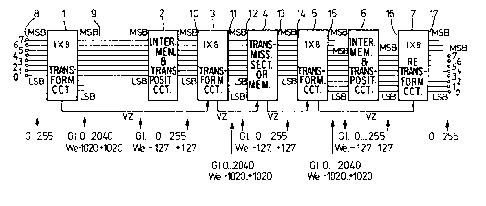
Figure 1 is a circuit arrangement for transforming
digital signals from the original range into a frequency range,
with a limitation of the place number and with ~ubsequent
retransformation into the original range;
132~
-- 5 --
Figure 2~sa circuit arrangement corresponding to figure 1,
although with additional range-shifting circuitry.
The transformation circuit that is shown in figure 1 is suitable
for processing television signals, in which the television image
is broken down into square blocks of 8 x 8 pixels and the scan
values that correspond to the luminance and/or chromonance
values are available as eight-place data words, with a
quantization of 256 quantization stages. Because of the
two-dimensional extent of the blocks, a two-dimensional
transformation is undertaken, when first a horizontal first
dimension and then a vertical second dimension is transformed.
In order to carry out this transformation, the circuit includes a
first transformation circuit 1, an intermediate memory and
transposition circuit 2, a second transformation circuit 3, and,
after a transmission section 4 or a mass memory, a circuit for
the retransformation, consisting of a third transformation
circuit 5, a second intermediate memory and transposition circuit
6, and a fourth transformation circuit 7. The four
transformation circuits 1, 3, 5, and 7 can be configured, for
example, as memories, within the storage places of which all the
transformed values, obtained with the transformation function,
are contained and during addressing their inputs are applied to
the outputs. The intermediate memory and transformation circuits
2 and 6 can be configured as memories, in which the sequence of
:
.. .
-` 1 3 2 ~ 5
-- 6 --
the stored values is so regrouped that the values previously
~ contained in the lines and in the columns, and vice versa, are
i reversed. The matrix that forms the coefficients is thus rotated
through 90.
Beneath the function blocks, in each instance, the value range
that the scan values or, after transformation, the DC components
and the AC components of the transformed coefficients, occupy is
given in decimal form.
The scanning values at the input 8 occupy a word range from 0 to
255. Assuming that eight pixels of an 8 x 8 matrix are
transformed in the first dimension, the place number at output 9
of the transformation circuit 1 increases by the factor 8. This
means that at output 9 the value range includes the number values
,, ~ 0~ ~o7v /a~
A from 0 to~- 04~ for the DC component and from -1.020 to +1.020
for the AC components. By not considering the three lowest value
places (LSB) the coefficients are divided by eight. This place
number also forms the basis of the values at input 10 of the
second transformation circuit 3, whereupon the transformed
coefficients at output 11 are once again increased by the factor
8 and by non-consideration of the three lowest value places (LSB)
are restricted to the above discussed range of the DC component
and of the AC components.
.'.. '. ,
.
" . -
- 1 3 2 ~
-- 7 --
Iæ
Thus, at the input X of a transmission section 4 or a mass memory
for the DC component there are values with 256 gradations
available, although there are, however, only 128 gradations for
the AC components. The values for the AC components are thus
more coarsely quanticized and any errors in quantization are
perceived as noise during reproduction, in that during
progressive transitional changes in brilliance or colour,
staircase structures will become visible.
After storage and the transmission, the transformed values at the
output 13 are transformed back into the image range, this being
done in the reverse manner to the initial transformation. The
retransformation back is effected first unidimensionally in the
columns. After transformation back from the data words at the
input 14, at output 15 data words are computed, the value range
of which for the DC components and for the AC components is in
each instance between -1.020 and +1.020, with the actual occupied
value range only extending from +255 and -255, since the higher
binary places are equal to zero. For this reason, the three
highest value places do not need to be taken into account. Of
the quoted value range, a DC component occupies between 0 and 255
and AC components occupy between -127 and +127. After the rows
and columns have been exchanged in the intermediate memory and
the transposition circuit 6, the data words of this value range
pass to the input 16 of the fourth transformation circuit 7.
After retransformation, at the output 17 of the fourth
1 3 ~
-- 8 --
transformation circuit 7 there are once again data words, of
which the highest value places (MSB) are not taken into account.
The value range of the scan value once again amounts to between 0
and 255.
In the circuit shown in figure 2, which is constructed like that
shown in figure 1, there are additional range-shift circuits 18
and 19, which can be configured, for example, as addition
circuits of a variable value with a constant value. During
processing of the DC component in the stili unrestricted place
number, the value of the relevant DC component at the input 20,
is subtracted with half of its maximum number range, which is to
say at 2.040 with 1.020, so that the new value range at output 21
is now between -1.020 and +1.020. This means that the value
range of the DC component coincides with that of the AC
component. In place of division by 8 by elimination by the three
lowest value places (LSB) here only a division by 4 is effected.
The negative number range of the DC component that is now
possible is characterized by a sign in the same way as in the
case of the AC components.
This is to the benefit of the AC components, which can now be
processed at a resolution of -255 to +255 in the transformation
circuit 3. In the subsequent stages, the further transformation
and the retransformation corresponds to those from figure 1.
After retransfor~ation of the second dimension it is, however,
.
' , ,
:, .
9 132~ 5
necessary to re-establish the original range. This is done by
the further range shift circuit 19, in which the numerical value
255 is added to the data words at input 21, and the result is
divided by 2. At output 23 one can then pick off a data word,
the value range of which extends from O to 255. Using the method
described, and without increasing the place number, one can
achieve the fact that the AC components can be stored or
transmitted at a resolution that is enhanced by the factor 2 and
this leads to a finer and less obvious gradation of the luminance
- and chromonance during reproduction of the values in the original
range.
: .