Note: Descriptions are shown in the official language in which they were submitted.
-
1326~59
THERMAL IMAGING DEVICE
This invention relates to thermal imaging devices and in
particular to thermal imaging devices comprising an array of
pyroelectric detector elements responsive to infra-red radiation.
The main factor limiting the performance of existing
pyroelectric imagers is the thermal conductance between ad~acent
detector elements and between each detector element and the
supporting snd interrogating structure.
U.K. Patent Application No. 2163596A dlscloses a thermal
imaglng devlce comprislng a ferroelectrlc slab bearing a common
electrode on one maln surface ~nd a signal electrode structure on
the opposite maln surface. The signal electrode structure 18
electrlcally connected to electrodes of a clrcuit substrate by
means of conductors. The transverse heat conduction between
adjacent conductors is reduced by incorporating each conductor on
a bore in a respective pillar of thermally insulating material,
the pillars also being effectlve to suppoct the ferroelectrlc slab.
It is an ob~ect of the present invention to provide an
alternative thermal imaging device in which the pyroelectric
detector elements are supported by pillars, but wherein the
thermal losses between the detector elements and supporting
pillars are reduced.
q~
~ A
,........................................................ .
'
: 2 : 1326~
According to a first aspect of the present invention a
thermal imaging device comprises: a layer comprising pyroelectric
material; an array of inter-connected electrodes carried on one
major surface of the layer; an array of discrete electrodes
carried on the other major surface of the layer; a plurality o
pillars effective to support the layer and to enable the passage
of electrical signals between the discrete electrodes and an
electrical signal processing means, each pillar being located on
an electrical contact region within a nonelectroded region of said
other major surface within a respective discrete electrode, the
contact region and discrete electrode being electrically connected
by a respective elongate region of electrically conductive
material extending over said nonelectroded region.
The layer may comprise a continuouæ film of pyroelectric
material, for example, a pyroelectric polymer.
Alternatively the layer may comprise an array of discrete
reglons of pyroelectric material carried on a continuous film of
dlelectric material. ~xamples of suitable pyroelectric materials
are lead lanthanum zlrconium titanate, lead zirconium titanate,
lead titanate and barium titanate.
The pyroelectric material suitably comprises polyvinylidene
fluoride (PVDP) or a copolymer of vinylidene fluoride with, for
example, trifluoroethylene (P(VDF-TrFE)).
The pyroelectric material in the device may comprise material
which is inherently pyroelectric, or material whose pyroelectric
characteristics are induced (e.g. by appropriate poling of
ferroelectric material).
The elongate region suitably has a length to width ratio of
at least 5.
In a preferred embodiment, said array of inter-connected
electrodes comprises an array of electrically conductive regions
carried on sald one surface at positions corresponding to the
positions of the discrete electrodes on the other surface, said
electrically conductive regions being inter-connected by
electrical conductors which are narrow compared with the width of
i the electrically conductive regions.
.,
~;
A~'`
,
'
: 3 : 132~
According to a second aspect of the present invention a
process for making a thermal imaging device comprises: forming a
layer comprising pyroelectric material; forming an array af
discrete electrodes on one major surface of the layer, each
discrete electrode substantially surrounding a nonelectroded
portion of the one surface; forming electrically conductive
contact regions within the nonelectroded regions together with an
elongate region of electrically conductive material extending over
the nonelectroded region and electrically connecting each discrete
electrode to a respective contact region; forming respective
electrically conductive support pillars on each contact region;
connecting the support pillars to the input terminals of a signal
processing means; and forming an inter-connected electrode
structure on the other major surface of the layer, at positions
aligned with the array of discrete electrodes.
Where the layer is a pyroelectric polymer, the step of
forming a layer suitably comprises: spin-coating a layer of a
polymer on an electrically conductive substrate; treating the
polymer such that it is made pyroelectric; and dissolving away
the substrate before forming the inter-connected electrode
structure on the other ma~or surface of the layer.
Where the layer comprises an array of discrete regions of
pyroelectric material carried on a continuous film of dielectric
material, the inter-connected electrode structure is formed on one
surface of the dielectric material; and the step of forming a
layer comprise~: forming an array of regions of pyroelectric
; material on the inter-connected electrodes and exposed regions of
the one surface of the dielectric film.
The optimum thickness of pyroelectric materials in hybrid
structures of low thermal conductance is of the order of one
micron. The thermal conductance of metal electrodes dominates
; that of a pyroelectric material one micron thick even if the metalfllm is only 0.03 micron, the thickness below which gold films
become discontinuous. The use of a long, narrow electrical
conductor to connect each pillar and discrete electrode ensures
that the thermal conductance from the respective pixel to the
support pillar is small.
.
,:
: 4 : 1326~5~
Two thermal imaging devices in accordance with invention
together with methods for fabricating the devices, will nbw be
described, by way of example only, with reference to the
accompanying drawings of which:
Figure 1 shows a section of the first thermal imaging device
Figure 2(a) is a schematic sectional view of part of a
surface of the device of Figure 1 illustrating the discrete
electrodes;
Figure 2(b) is a schematic sectional view corresponding to
Figure 2(a) illustrating a modifed arrangement;
Figure 3 shows a plan view of the device illustrating the
inter-connected electrode arrangement; and
Figure 4 shows a section of the second thermal imaging device.
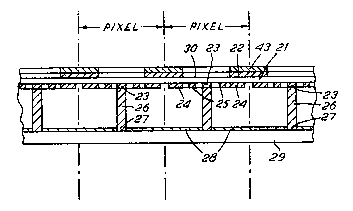
Referring eirstly to Figures 1 and 2(a), a pyroelectric film
21 of, for example, P(VDF-TrF~) has a pattern of inter-connected
electrodes 22 formed on one side and an array of discrete
electrodes 24 on the other side. Electrically conductive pads 23
are connected by respective narrow electrically conducting strip
25 which passes almost completely round the pad 23 to the
surrounding discrete electrodes 24. Pillars 26 are attached at
one end to pads and at the other end to lnput pads 27 of an
integrated circuit 28 formed on the substrate 29. Thus thermal
insulation is provided by the gap 3i between each pad 23 and
surrounding discrete electrode 24 . A gap 32 separates ad~acent
pixels. Pigure 2(b) ~hows an alternative arrangement of the
structure carried on the second ~ide of the film 21. This again
comprises a pad 23, a gap 31 around the pad and a discrete
electrode 24. The electrode 24 i8 however linked to the pad 23
by a narrow electrically conductive linear strip 33 which extends
almost to the edge of the discrete electrode 24.
Figure 3 shows a plan view of the inter-connected electrodes
shown at 22 in Figure 1. The inter-connected electrodes each
have a central hole 30 in the area corresponding to the pads 23
; and to the gap 31 within the discrete electrodes 24 shown in
Pigures 2(a) or 2(b). The central hole 30 ensures that the
inter-connected electrodes do not increase the thermal conductance
between the pads 23 and discrete electrodes 24. ~urthermore, the
.' f~
., ~
132~
thermal conductance from pixel to pixel is kept low by the use of
a thin pyroelectric film and by the gap 41 between adjacent pixel
areas of the inter-connected electrodes, electrical continuity
being provided by narrow conducting strips 42 across the gaps
~1. The inter-connected electrodes will generally be covered by
an infra-red absorbent layer 43, for example a layer of black
gold, platinum black, or a metal-dielectric-metal sandwich
structure. Alternatively, if the discrete electrode-pyroelectric
film-interconnected electrode layers together comprise a 1/4
wavelength thickness for infra-red radiation (i.e. about 1.5
microns) this structure itself will constitute an efficient
thermal absorber.
The second device to be described is shown in Figure 4, in
which corresponding features of those of the first device are
correspondingly labelled. A dielectric film 51 has a pattern of
inter-connected electrodes 22 formed on a surface. An array of
discrete pyroelectric regions 52 is formed on the electrodes 22
and the dielectric film 51 whece exposed and an array of discrete
electrodes formed on the pyroelect;ic elements. The
lnter-connected electrodes 22 and the discrete electrodes 24
surrounding a central conductive pad and conducting strips 25 are
similae to those described hereinbefore with reference to Figures
3 and 2 respectively. The arrangement of the pillars 26,
integrated circuits 28, ~ubstrate 29 and infra-red absorbant layer
43 18 similar to that de~cribed hereinbefore with reference to
Figure 1.
The pyroelectric regions may be again formed, for example,
from a pyroelectric polymer, or may, for example, be formed from a
ferroelectric ceramic material.
Two proce~ses for making a thermal imaging device, the first
relevant to the device shown in Figure 1, and the second relevant
to the device shown in Figure 4, will now be described. In the
first process it is assumed that the pyroelectric film 21 is a
copolymer of polyvinylidene fluoride ~PVDP), but any thin
self-supporting pyroelectric material could be employed. In the
first process an optically flat electrically conductive substrate
: 6
1326~9
is spin-coated with polyvinylidene fluoride-trifluoroethylene
copolymer tvDF-TrFE). The substrate might be a silicon wafer, or
any material which can be etched or dissolved away in a subsequent
process. The VDF-TrFE copolymer may be dissolved in a mixture of
acetone and dimethyl formamide~ or in one or more of several
possible solvents for VDF copolymers. The spin-coated polymer
layer is chosen to be an optimum thickness for the infra-red
detection application, and will be typically 1 micron thick.
The polymer membrane is made pyroelectric by any standard
techniqae such as by corona poling.
A gold pattern of discrete electrodes 24, pads 23 and strips
25 such as those shown in Figure 2a is then formed on the
pyroelectric fllm 21 by standard photolithographic techniques.
This will be referred to as the bottom electrode. The pattern
repeat distance is typically 100 microns and the gold thickness
0.03 microns. Each element of the pattern will be referred to as
a pixel, with a typical array having at least 100 x 100 pixels.
The strips 25 will typically be 3 microns wide.
The gap region 31 of the electrode ~60 microns in external
diameter) around the centre region provides the thermal isolation
between the centre region 23 and the active thermal detection
region 24 of each pixel.
Gold support pillars - typically 25 mlcrons diameter and 25
microns high - are grown by standard photolithographic and
electroplating techniques on the input pads 27 of an integtated
circuit 28. Figures 1 and 2a show the position where the pillars
connect to the discrete electrode pattern.
The whole device is then inverted on to a complementary
electronic measurement circuit on a silicon chip 29, and
electrical connection made to the gold pillars, for example by
soft solder.
The original substrate material is etched or dissolved to
leave the polymer layer supported by the gold pillars.
The inter-connected electrodes are formed by standard
photolithographic techniques on the exposed side of the
pyroelectric fllm 21. The inter-connected electrode pattern
r
r
~.
r
.
.
regi~ters with the discrete electrodes so that the central regions
of pyroelectric film 21 are left unelectroded. These regions
provide the thermal isolation between the pillars and the active,
electroded, outer region of each pixel~
An additional infra-red absorbing layer may also be deposited
in the same pattern and position as the inter-connected electrode
structure. The thermal mass of the inter-connected electrodes
and absorbing layer will, in general, be greater than that of the
discrete elPctrodes but this extra material will not increase the
conductance between detector and silicon chip.
In the second process for making a thermal imaging device in
accordance with Figure 4 a pattern of inter-connected electrodes
is formed by standard photolithographic techniques on a thin film
of a dielectric (for example polyimide, silicon oxide, silicon
nitride or silicon oxy-nitride). This inter-connected electrode
pattern is of the form illustrated in Figure 3 and carries an
infra-red absorbing material, such as black gold.
The inter-connected electrode pattern is spin-coated with
polyvinylidene fluoride-trifluoroethylene copolymer (P(VDF-TrFe)),
which might be dissolved in a mixture of acetone and dimethyl
formamide, or in one or more of several possible solvents for VDF
copolymers. The spin-coated polymer layer i~ chosen to be an
optimum thickness for the infra-red detection application, and
will be typically 1 micron thick and is formed as an array of
discrete elements of the copolymer as shown in Figure 4.
The polymer membrane or elements are made pyroelectric by any
standard technique such as by corona poling.
A gold pattern of discrete electrodes, pads, and
inter-connecting strip such as the one shown in Figure 2a is then
formed on the pyroelectric elements by standard photolithographic
techniques. The pattern repeat distance is typically 100 microns
and the gold thickness 0.03 microns. each element of the pattern
will be referred to as a pixel, and a typical array has at least
100 x 100 pixels.
A Sold track typically 3 microns wide, connects each pad 23
to the discrete electrode 24. The gap region 31 of the electrode
~ 8 : 132~
(60 microns in external diameter) around the centre region
provides the thermal isolation between the centre region 23 and
the active thermal detection region 24 of each pixel.
Gold support pillars - typically 25 microns diameter and 25
microns high - are grown by standard photolithographic and
electroplating techniques on the input pads of an integrated
circuit.
The whole device is then inverted on to the complementary
electronic measurement circuit on a silicon chip Z9, and
electrical connection made to the gold pillars, for example by
soft solder.
The embodiments described hereinbefore are given by way of
example only to illustrate how advantage can be taken of the low
thermal conductance both between adjacent detector elements,
resulting from the use of gaps between the interconnected
electrodes and the use of thin pyroelectric films (with or without
thin dielectric films), and also between elements and the
supportive pillars, resulting from the use of gaps between the
pads and dlscrete electrodes and the use of central holes in the
inter-connected electrodes.
A