Note: Descriptions are shown in the official language in which they were submitted.
~- 1 326069
MICROWAVE LANDING SYSTEM
BACXGROUND OF THE INVENTION
The present invention relates to a microwaYe landing system
(MLS) and, more particularly, to an MLS in which a beam
scanning antenna is provided with an amplifying function to
5 serve as an active array and a tratitional amplifier is omitted to
enhance reliable operations.
An MLS has customarily been constituted by an elevation
(EL) guidance equipment and an azimuth ~AZ) 8uidance
equipment with or without the addition of a back EL (BAZ)
10 guidance equipment. The EL guidance equipment and AZ
guidance equipment are essentially similar in construction to each
other except for the arrangement of a beam scanning antenna.
Specifically, while the beam scanning antenna of the AZ guidance
equipment forms a vertically wide and horizontally narrow fan
15 beam and moves it in a reciprocating motion in the azimuthal
direction, the beam scanning antenna of the EL guidance
equipment forms a horizontally wide and vertically narrow fan
beam and reciprocatingly moves it in the elevational direction.
The A2: guidance equipment and the EL guidance equipment are
20 equipped with six auxiliary antennas and two auxiliary antennas,
1 326069
--2--
respectively. Both of the AZ guidance equipment and EL
guidance equipment are made up of a controller for generating a
system sync signal which governs the timings of the entire
system and a timing signal which determines the operation
5 timings of the guide itself, an exciter for generating a signal
having a predetermined frequency to be used by the Ml,S and
modulating a preamble of transmission timings by DPSK
tDifferential Phase Shift Keying) according to a predetermined
sequence, a power amplifier for amplifying a high frequency
10 signal generated b~r the exciter to a predetermined output, and
an antenna switching unit for selectively feeding power to
antennas. Each beam scanning antenna is generally implemented
by a phased array. Specifically, each beam scanning antenna is
made up of a power divider for dividing transmission power by a
15 predetermined ratio, phase shifters for effecting phase shifts for
beam scanning, and radiating elements.
The prior art MLS having a beam scanning antenna which is
implemented as a phased array is provided with redundancy.
Howe~er, a power amplifier, antenna switching unit and the like
20 which are included in each of the AZ and EL guidance equipments
and are the key to the reliability of operation are not provided
with redundancy. Especially, when the system is constructed in
a dual configuration, it is extremely difficult to provide the
ant~nna switching unit with redundancy and therefore to enhance
25 the reliability of operation.
- 1 32606q
--3--
SUMMARY OF THE INYENTION
It is therefore an object of the present invention to provide
an MLS operable with high reliability and continuously over a
long period of time.
It is another obiect of the present invention to Provide an
MLS capable of feeding power to antennas with a minimum of
loss.
It is another obiect of the present invention to provide a
generally improved MLS.
A microwave landing system for feeding predetermined power
to an auxiliary antennas of the present invention comprises a
power divider for dividing power in a distribution ratio which is
associated with ~ radiating elements of a beam scanning
antenna, n phase shifters individually associated with the 7~
radiating elements for proviting fractions of the divided power
with phases for effecting beam scanning, ~ variable attenuators
individually associated the 7~ phase shifters for providing outputs
of the phase shifters ~vith attenuations of predetermined
characteristics which are variable depending upon whether or not
2 0 a beam scanning timing is reached, 7t power amplifiers
individually associated with the ~ variable attenuators for
amplifying outputs of the variable attenuators to a
predetermined level, ~s ~Ç dividers individually associated with the
7~ power amplifiers for dividing outputs of ths power amplifiers
2 5 into two and each feeding one of resulting two outputs to the
1 326069
--4--
radiating element associated with the ~ divider, the 3~ dividers
each comprising two p-i-n diodes individually connected between
opposite output terminals and ground and turning off the p-i-n
diodes connected to the radiating element and turning on the
5 other p-i-n diode at a beam scanning timing, and a power
combiner for combining the other output of the 7~ ~Ç dividers
bein~ not connected to the radiating elements and delivering a
resulting combined signal to an auxiliary antenna located outside
of the ~ radiating elements.
BRIEF DESCRIPTION OF THE DRAWINGS
The above and other objects, features and advantages of the
present invention will become more apparent from the following
detailed desc,ription taken with the accompanying drawings in
15 which:
Fig. 1 is a schematic block dia8ram showing a prior art
MLS i
Fig. 2A shows transmission timings;
Fig. 2B shows the format of sequences #1 and #2 shown in
20 Fig. 2Ai
Fi. 3A shows AZ transmission timings shown in Fig. 2B;
Fig. 3B shows EL transmission timings also shown in
Fig. 2B;
Fig. 4 is a schematic block diagram showing an MLS
25 embodying the present invention;
1 326069
--5--
Fig. 5 is a plot useful for understanding the opeation of
~ariable attenuators included in the embodiment of Fig. 4;
Fig. 6 is a diagram schematically showing a specific
construction of the variable attenuators; and
Fig. 7 is a diagram schematically showing another specific
construction of the Yariable attenuators.
1 326069
--6--
DESCRIPTION OF THE PREFER~ED EMBODIMENT
To better understand the present invention, a brief reference
will be made to a prior art MLS.
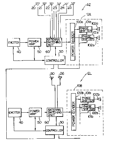
As shown in Fig. 1, a prior art MLS is implemented by an AZ
5 guidance equipment and an EL guidance equipment with or
without the addition of a back AZ (BAZ) guidance equipment.
The AZ guidance equipment and EL guidance equipment are
essentially similar in construction to each other except for the
arrangement of an antenna. The AZ guidance equipment and the
10 EL guidance equipment are equipped with beam scanning
antennas 1 OA and 1 OB, respectively. Specifically, while the
beam scanning antenna 10A of the AZ guidance equipment forms
a vertically wide and horizontally narrow fan beam and moves it
in a reciprocating motion in the azimuthal direction, the beam
15 scanning antenna 1 OB of the EL guidance equipment forms a
horizontally wide and vertically narrow fan beam and
reciprocatingly moves it in the elevational direction. The AZ
guidance equipment is further proYided with a data antenna 20,
a left OCI (Out of Coverage Indication) antenna 21, a right OCI
20 antenna 22, a rear OCI antenna 23, a right clearance antenna
24, and a left clearance antenna 25. On the other hand, the EL
guidance eq~ipment is pro-~ided with a data antenna 2 0 and an
OCI antenna 2 6. A current trend in the art is toward the
omission of OCI antennas, and even clearance signals associated
25 with the clearance antennas may be transmitted via beam
1 32606q
scanning antennas. Presumably, therefore, each of the AZ and
EL guidance equipments v~ill be equipped with a sin~le auxiliary
antenna, i. e., data antenna in the future. The prior art ~LS
will be outlined taking the AZ guidance equipment for example~
The entire MLS uses the same frequency and, as shown in
Figs. 2A and 2B, sends predetermined signals via the
independent antennas on a time division basis. Specifically,
Fig. 2A shows the transmission timings of the MLS while Fig. 2B
shows the formats of sequences ~SEQs) #1 and #2 shown in
Fig. 2A. As shown, the transmission timings of the MLS are
defined by four blocks of SEQ #1 and four blocks of SE~2 #2. At
a normal rate, each of the blocks involves a single AZ timing
and tkree EL timings. Figs. 3A and 3B illustrate respectively the
AZ transmission timing and the EL transmission timing which are
shown in Fig. 2B. As shown in Fig. 3A, the AZ timing is made
up of the timings of a preamble sent over the data antenna, OCI
signals individuallY sent over the right, left and rear C)C~
antennas, clearance signals individually sent over the right and
left clearance antennas or the beam scanning antenna lOA, and
2 0 a beam scanning signal sent over the beam scanning antenna
lOA.
Referring again to Fig. 1, The AZ guidance equipment
includes a controller 3 0 for generating a system sync signal
which governs the timings of the entire system and a timing
signal which determines the operation timings of the AZ guidance
1 326069
--8--
equipment. An exciter 40 generates a signal of 5 gigahertz to be
used by the MLS and modulates a preamble by DPSK in a
predetermined sequence. A power amplifier 50 amplifies a high
frequency signal generated by the exciter 40 to a predetermined
level. An antenna switching unit 60 selectively applies power to
the antennas according to a sequence which is determined by the
controller 3 0 . Usually imPlemented by a phased array, the
beam scanning antenna 1 OA is comprised of a power divider
lOOa for dividing the transmission power by a predetermined
division ratio, phase shifters lOla for effecting phase shifts for
beam scanning, and radiating elements 102a. Generally, the
auxiliary antennas 2 0 to 2 5 are each constructed into a
waveguide slot array having a reflector. Likewise, the beam
scanning antenna lOB of the EL guidance equipment is made up
of a power divider lOOb, phase shifters lOlb, and radiating
elements 102b. The EL guidance equipment is operated in
substantially the same manner as the AZ guidance equipment
except for the directivity characteristics defined by the radiating
elements 10 2 b.
The prior art MLS having a beam scanning antenna which is
implemented as a phased array is provided with redundancy.
However, a power amplifier, antenna switching unit and the like
which ~re included in each of the AZ and EL guidance equipments
and are the keY to the reliability of operation are not provided
25 with redundancy. Especially, when the system is constructed in
-9- 1 32606q
a dual configuration, it is extremely difficult to provide the
antenna switchin~ unit with redundancy and therefore to enhance
the reliability of operation.
Referring to Fig. 4, an MLS embodying the present invention
5 is shown and generally designated by the reference numeral 100.
The system is not provided with OCI antennas because OCI
antennas will be disused in the future, as discussed earlier. In
the figure, there are shown an exciter 110, a ~ower divider
120, ~2 phase shifters 130, ~2 variable attenuators 140, ~ power
amplifiers 150, ~2 ~ dividers 160 each having PIN diodes 162 and
164, ~2 radiating elements 180, and a data antenna 190.
The exciter 110 produces an MLS signal which has been
modulated by DPSK in a predetermined format and delivers it to
the power tivider 120. In response, the power divider 120
15 equally divides the MLS signal and feeds the resulting fractions to
the 7~ phase shifters 130. Outputs of the phase shifters 130 are
individually applied to the variable attenuators 140 which sets up
a Taylor distribution or the like at a bea.m scanning timing and a
uniform amount of attenuation at the other timings. More
2 0 specifically, the variable attenuators 14 0 provide attenuations
which are distributed as represented by a curve ~ in Fig. 5 at a
TO scan timing and an FRO scan timing of Figs. 3A and 3B,
thereby setting up a Taylor distribution of the like. At the other
timings, the variable attenuators 140 provide a uniform and
Z 5 minimum amount of attenuation as represented by a line b in
-lO- 1 326069
Fig. 5. Conc~rning the "~" radiating element, the variabl~
attenuator 140 connected to this particular radiating element
effects attenuation by any of the amounts A and B shown in
Fig. 5. The attenuation B differs from one radiating element to
5 another. As shown in Fig. 6, the simplest form of the variable
attenuator 140 is the combination of fixed attenuators 144 and a
p-i-n diode switch 142. In this case, however, the fixed
attenuators 144 connected to any particular radiating element
180 have to be so selected as to effect an attenuation which is
10 different from attenuations of the others. Fig. 7 shows an
alternative ~ariable attenuator 140B having multiple variable
attenuators 140A of Fig. 6 which are cascaded in consecutive
steps and having a capability for digitally changing the amount
of attenuation as needed. With the configuration shown in
15 Fig. 7, it is possible to implement all of the variable attenuators
associated with the beam scanning antenna of the illustrative
embodiment with a single variable attenuator. The variable
attenuator 140B shown in Fig. 7 is capable of varying the
- amount of attenuation over a range of 0 dB to 15 dB by 1 dB
2 0 steP.
The signals each being attenuated by a respective one of the
variable attenuators 140 are fed to their associated power
amplifiers 15 0 to be thereby amplified to desired power. The
outputs of the amplifiers 150 which are set up based on the MLS
25 technical standards are less than 2 W, even taking account of
1 326o6q
the loss of a power combiner 170 which will be described. The
power amplifiers 150 remain inoperative except for the radiating
timings of the device (i. e. TO scan timing, FRO scan timin~,
clearance timing and preamble timing shown in Figs. 3A and 3B;
5 OCI antennas being omitted in the illustrative embodiment). The
outputs of the power amplifiers 150 are fed to their associated ~
dividers 160 each having the p-i-n diodes 162 and 164 at
opposite output terminals thereof. At the beam scanning
timings, i. e., TO scan, FRO scan and clearance timings shown
in Figs. 3A and 3B, ~he p-i-n diodes 164 are turned on while the
p-i-n diodes 162 are turned off. When the characteristic
impedances and electrical lengths of the branches of each ~
divider 160 are adequately selected, power routed to the p-i-n
diode 164 will be totally reflected by the p-i-n diode 164 toward
15 the radiating elements 180. Conversely, at the timing for
feeding power to the data antenna, the p-i-n diodes 162 are
turned on and the p-i-n diodes 164 are turned off. At this
instant, the outputs of the power amplifiers 150 are applied to
the power combiner 170 with a minimum of loss. When signals
20 are to be applied to the power combiner 170, the amounts of
attenuation effected by the variable attenuators 140 become
equal and, yet, the phase shifters 130 control the inputs thereto
to uniformize them with respect to phase. The power combiner
170 may be implemented by an ordinary combiner having
25 multiple inputs and one output.
-12- l 326069
In summary, it will be seen that the present invention
provides an MLS capable of feeding output signals to radiating
elements and a power combiner with a minimum of loss. This
unprecedented advantage is achieved by constructing a beam
5 scanning antenna into an active array, connecting the outputs of
phase shifters each being associated with a respective one of
radiating elements to ~ dividers each having p-i-n diodes at
opposite output terminals, and turning on and off the p-i-n
diodes of each ~Ç divider alternately.
Further, in accordance with the present invention, a signal
source and a control section are each constructed in a dual
configuration to offer redundancy to all of the sections. The
system is therefore capable of operating with significant
reliability and continuously over a long period of time.
Various modifications will become possible for those skilled
in the art after receiving the teachings of the present disclosure
without departing from the scope thereof.