Note: Descriptions are shown in the official language in which they were submitted.
1 32628~
The present invention relates to a picture quality
adjusting circuit for use in a video signal processing
apparatus, and, more particularly, to a picture quality
adjusting circuit which uses a finite impulse response
(FIR) filter to realize both of contour compensation and
noise canceling with a single circuit.
A video signal processing apparatus that processes
video signals of an NTSC system has a contour compen-
sator and a noise canceling circuit or the like incor-
porated therein, the former for emphasizing the contour
of a video image and the latter for reducing a noise
component included in a video signal.
- The contour compensator controls the gain of asignal of a frequency around 1 to 2 MHz, most sensible
to the vision of human beings, in order to emphasize the
contour of a picture. An example of the contour compen-
` sator has first and second differentiation circuits for
~; acquiring a secondary differential waveform from an
; input signal, and a delay circuit for delaying the input
- 20 signal. The output of the second differential circuit
- is inverted by an inverter and the inverted signal is
r,~i
added with the delayed, input signal, thereby providing
a contour-compensated signal.
An example of the noise canceling circuit has
a high-pass filter for extracting a high-frequency com-
ponent from an input signal, a limiter for extracting a
noise component by limiting the level of the output of
-
'` ~ .
''
~ 326~8~
the filter, and a delay circuit for delaying the input
signal. The noise component from the limiter is inverted by
an inverter, and the resultant signal is added with the
delayed, input signal, thereby providing a signal with the
- 5 noise component canceled out.
;- The aforementioned conventional contour compensator is
constituted by an analog circuit. In effect, therefore, the
secondary differential waveform acquired from the contour
compensator, for example, may include a ringing and the
accurate contour compensation cannot be thus performed.
Since the contour compensation is performed only on a
lu~inance (Y) signal in order to protect a color (C) signal,
` it is necessary to provide the contour compensator at thesucceeding stage to an Y/C separator. This restricts the
circuit design.
Further, the conventional picture quality adjusting
circuit requires the contour compensator and noise cancelling
circuit arranged separately, thus enlarging the overall
circuit configuration.
This invention provides: a picture quality adjusting
circuit with a compact circuit configuration; a picture
quality adjusting circuit for executing an accurate picture
quality adjustment; and a picture quality adjusting circuit
which is substantially relieved of restriction on circuit
design.
, .
, .
. . ~
:.~
''
- 2 -
P~
;
--` 1 326289
According to one aspect of this invention, there is
provided a circuit for adjusting picture quality by
processing a video signal, said circuit comprising:
filter means for receiving said video signal and
extracting a high-frequency component therefrom;
waveform-shaping means for wave-shaping said high-
frequency component extracted by said filter means into a
noise cancelling signal for cancelling a noise; and
adder means for adding said video signal and said noise
cancelling signal wave-shaped by said waveform-shaping means
to provide a signal with adjusted picture quality.
According to a further aspect of this invention there is
provided a circuit for adjusting a picture quality by
processing a digital video signal, said digital video signal
including a noise, comprising:
digital filter means for receiving said digital video
signal and extracting a high-frequency component therefrom;
first waveform-shaping means for wave-shaping said high-
~- frequency component extracted by said digital filter means to
provide a noise cancel signal for canceling the noise;
second waveform-shaping means for wave-shaping said
high-frequency component extracted by said digital filter
means to provide a contour compensation signal for
compensating a contour of a picture; and
adder means for adding said digital video signal, said
noise cancel signal from said first waveform-shaping means
. and said contour compensation signal from said second
waveform-shaping means to provide a signal with adjusted
picture quality.
. 30
';
- 3 -
~, .
, .
~ 326~89
The foregoing aspects and other features of the
invention will be more fully explained in the following
description in conjunction with the accompanying drawings
wherein:
Fig. 1 is a circuit diagram illustrating the
configuration of a picture quality adjusting circuit
according to one embodiment of this invention;
Figs. 2A through 2E are diagrams illustrating signal
~; waveforms in individual sections of the circuit shown in Fig.
~', 10 1; -'
Fig. 3 is a diagram illustrating the circuit
configuration of an FIR filter shown in Fig. l;
Fig. 4 is a diagram illustrating the frequency
:,
''
' .
r.~
~ 20
~, .
:,
~ 25
,
- - 3a -
E~
, ,
'-` 1 32628q
-- 4 --
characteristic of the filter shown in Fig. 3;
Figs. 5A through 5C are diagrams illustrating how
; gains for contour compensation and noise canceling are
changed by an external adjustment; and
Fig. ~ is a diagram illustrating a specific con-
~, figuration of the circuit shown in Fig. 1.
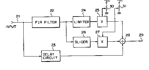
Fig. 1 illustrates one preferred embodiment of this
, invention.
- An input terminal 21 is supplied with a video
. .
signal of an NTSC system which is quantized as a digital
video signal, as shown in Fig. 2A. As should be obvious
from this diagram, the video signal includes a noise
; component as a high-frequency component. The video
;~ signal is supplied to an FIR filter 22 for extraction of
~;~` lS the high-frequency component as well as to a delay cir-
cuit 23. This delay circuit 23 serves to match the
,,;:
~- timings at which the quantized video signal is added
;, with a contour compensation signal and a noise canceling
,, .:
signal (the latter two signals will be described later).
Fig. 2B illustrates the output waveform from the
r. ~^
FIR filter whose configuration will be described in
- detail below. It should be noted from the diagram that
.~
the output of the FIR filter 22 includes an inverted
noise component and a secondary differential waveform
component. The latter waveform component is used to
emphasize the contour of a picture. The output of the
~- FIR filter 22 is supplied to a limiter 24 as well as to
:
: ,
,
,' ~
- t 32628q
a slicer 26. The outputs of the limiter 24 and slicer
26 are respectively supplied to multipliers 25 and 27,
serving as amplifiers, for gain adjustment of these out-
puts. The gain adjustment may be externally executed by
; 5 means of variable resistors 30 and 31, etc.
~; The limiter 24 limits the output of the FIR filter
22 with a predetermined limit level and outputs a signal
~, with a waveform as shown in Fig. 2C. This output signal
is considered as a noise component and is used as a
noise canceling signal. The slicer 26 slices the output
of the FIR filter 22 with a predetermined slice level
and outputs a signal with a waveform as shown in
Eig. 2D. This waveform is a secondary differential
waveform and is used as a contour compensation signal.
. ,~
` 15 Those outputs of the limiter 24 and slicer 26 are
j~ supplied to an adder 28 where they are added with the
- quantized video signal (Fig. 2A) delayed by the delay
circuit 23. The adder 28 provides a signal (see
Fig. 2E) which has been subjected to contour compen-
sation and does not contain the noise component. The
-- output signal of the adder 28 is supplied to an output
, terminal 29.
Fig. 3 exemplifies the circuit configuration of the
FIR ~ilter 22. The quantized video signal supplied to
an input terminal 220 is supplied to a delay section 221
which is constituted by a plurality of series-coupled
delay elements. The output of the delay section 221 is
~,,
, ~ .
,
1 326~89
-- 6
;~ _
supplied to another delay section 222 having the same
structure as the former delay section 221. The signal
,
at the input terminal 220, the output signal of the
delay section 221 and the output signal of the delay
section 222 are respectively supplied to coefficient
.:
multipliers 223, 224 and 225 for their gain adjustments.
The adjusted signals are then supplied to, and added in,
an adder 226. Accordingly, the output signal of the
adder 226 has a waveform as shown in Fig. 2B. The indi-
vidual delay elements of the delay sections 221 and 222
: .
" are driven by a clock pulse of 4 fsc (fsc: frequency of
a color subcarrier signal).
As shown in Fig. 4, the frequency characteristic of
. .
~ the FIR filter 22 has a notching characteristic at
; 15 3.58 MHz, the frequency band of a chromatic signal.. :i
~ Accordingly, the gain for this particular frequency is
. .~reduced, so that no chromatic signal component is output
:~ from the FIR filter 22. It should be understood from,i,.~,
~ Fig. 4, however, that a signal component having a fre- . ~.
quency around 1 to 2 MHz is output from the FIR filter
:,,'-''
! ~ ~ 22.
" . . .
According to this invention, therefore, the effec-
.....
`- tive utilization of the characteristic of the FIR
i~ filter 22 provides a secondary differential waveform
: `~
having no ringing and thus provides an accurate contour
compensation signal. Since the present circuit is
constituted by a digital circuit, it is not sensible to
.,
,~
. . :
, . -
;, ,
` ~ 326289
-- 7
a change in temperature and is therefore capable of pro-
viding a stable compensation signal. Due to the rich
notching characteristic of the FIR filter 22, unlike in
the case of the prior art, the location of the filter 22
is not restricted to the succeeding stage to an Y/C
.
separating section. This gives the circuit design a
greater flexibility.
The signal component associated with the contour
:;
' compensation is a frequency component human beings can
~j 10 visually sense. If this frequency component should
include a noise component, therefore, it would certainly
affect the quality of a picture. According to this
invention, the use of the FIR filter 22 not only can
realize the contour compensation but can also eliminate
;~ lS a noise component.
- ,
- In addition, according to this invention, the FIR
: .
j- filter can be shared as a single circuit by both of the
;` noise canceling circuit and contour compensator, which
.,
require the respective, separate preceding circuits
according to the prior art.
;
Fig. 5A illustrates how the level of the output of
the slicer 26 for contour compensation is controlled by
externally adjusting the gain of the amplifier 27.
Fig. 5B similarly illustrates how the level of the out-
put of the limiter 24 for noise canceling is controlledby externally adjusting the gain of the amplifier 25.
Referring to Fig. 5A, the ratio of the level of the
-' ~
:;
i:
.,., , :
1 326289
input to that of the output is kept at 1 : l in a slice
level range, i.e., a small-input region. For the region
outside this slice level range, the gain of the ampli-
fier 27 is externally adjusted by means of a variable
S resistor 31 or the like. In other words, the greater
the gain, the sharper the contour of a picture to be
emphasized. Conversely, the smaller the gain, the
;` softer the picture contour to be emphasized. It should
; be noted from Fig. 5B that the gain is reduced to remove
10 the noise component in a limiting level range, but the
ratio of the level of the input to that of the output
is kept at 1: 1 for the other region. Accordingly, a
general characteristic as shown in Fig. SC can be
.
;
attained.
Fig. 6 exemplifies a more specific configuration of
:
the circuit shown in Fig. l; the same reference numerals
` as used in the latter diagram are used in the former to
specify the identical or corresponding elements.
The limiter 24 has a limiting level generator 241
20 and a comparator 242, which compares the limiting level
from the generator 241 with the level of the output of
~- the FIR filter 22 (see Fig. 2B). When the output of the
FIR filter 22 is smaller than the limiting level, this
output itself is selected by a switch 243. When the
25 output of the FIR filter 22 is greater than the limiting
level, on the other hand, the limiting level is
selected. The signal with the selected level is
::~
'
-
., - ' , '.
1 326289
~, g
amplified by the amplifier 25 serving as a multiplier
'':"
and is then supplied as a noise canceling signal to an
adder 281.
The slicer 26 includes a slice level generator 261
and a comparator 262, which compares the slice level
from the generator 261 with the level of the output of
the FIR filter 22. When the output of the FIR filter 22
is greater than the slice level, this output itself is
selected by a switch 263 and is then supplied to a
subtracter 264. When the output of the FIR filter 22 is
smaller than the slice level, the latter is selected.
: ^
The slice level is subtracted from the signal with the
! selected level in the subtracter 264 to thereby provide
a contour compensation signal. This compensation signal
is added with the noise canceling signal in the adder
281. The resultant signal is supplied to the adder 28
:,
~ where it is added with the quantized video signal
-~ supplied through the delay circuit 23 from the FIR
filter 22.
Although the FIR filter is used in the above embo-
diment, an analog filter may be employed as well to
produce sufficient contour-compensating and noise-
eliminating effects.
~ According to this invention, as described above,
; 25 the use of an FIR filter realizes contour compensation
and noise elimination with a single circuit, thus
.,
~ making the overall circuit configuration more compact.
;, `
~ .
, .
, ' ' `
- 'I 32628q
-- 10 --
Further, the use of the FIR filter can substantially
eliminate generation of a ringing so that an accurate
contour compensation signal can be acquired. Further-
more, unlike in the case of the prior art, the location
of the contour compensator is not restricted to the suc-
ceeding stage to an Y/C separator, which is advantageous
in designing the circuit. In addition, because of the
use of a digital circuit, the present picture quality
adjusting circuit is not affected by a temperature
change and is therefore highly reliable.
.
.
.,