Note: Descriptions are shown in the official language in which they were submitted.
TITLE OF THE INVENTION 1 ~ 2 ~ 9 7
Superconducting member
BACRGROIIND OF THE INVENTION
Field of the Invention
The present invention relates to the structure of a
superconducting member, and more particularly, it relates
to the structure of a superconducting member having
excellent superconductivity, which is unrestrictedly
formed on a substrate of an arbitrary base material.
Description of the Prior Art
In recent years, oxide superconducting materials
having perovskite structure, such as those of La-Sr-Cu-O
and Y-Ba-Cu-O, have been discovered in succession. Since
such discovery, many studieE have been made on these
materials, which are higher in critical temperature than
conventional superconducting materials such as alloys or
intermetallic compounds of Nb-Ti, Nb-Ge and the like.
Such oxide superconducting materials are typically
manufactured by powder sintering at present. For
example, a superconducting wire rod is provided by
filling powder of an oxide superconducting material in a
metal pipe and performing wire drawing. In order to form
a circuit, there has been proposed a method of kneading
powder of an oxide superconducting material with an
organic binder and printing the same. In either method,
~ .
.-.
132~976
the powder is shaped into a linear or layer member, to be
finally sintered. Thus, the powder member is inevitably
6hrunk in 6intering, and hence it i~ difficult to obtain
a final product of arbitrary configuration or size.
Every oxide superconductor heretofore discovered has
high crystal anisotropy, and it is necessary to orient
its crystal structure in order to obtain high critical
current density. However, it is difficult to provide
accurate orientation by sintering. Further, voids
inevitably occur upon sintering, and hence it has been
impossible to obtain an oxide superconductor having
satisfactory critical current density by sintering.
On the other hand, an oxide superconductor having an
arbitrary configuration can be easily obtained by
preparing a base material with excellent workability and
depositing a superconducting film on the same, in a
manner unlike the sintering process. In particular, such
a superconducting film can be made by a vapor phase film
process such as sputtering, which i8 excellent in crystal
controllability, to easily obtain a den~e film, as
effective means for obtaining a superconductor having
excellent properties.
In the ca3e of forming a thin film on the base
material, however, heating in an oxidizing atmosphere is
required for performing heat treatment after film
,. .
.. . . .
. :. , . - ~ .
132~976
formation or for heating the substrate during film
formation. Thus, the superconductivity tends to be
reduced by oxidation of the base material or diffusion
between a superconducting layer and the ba~e material.
In the method of forming a thin film on the base
material, therefore, the base material, therefore, the
base material is restricted to a high-priced material
which is hard to work, such as SrTiO3 or MgO.
In particular, formation of an oxide superconducting
film on a metal base material has not yet been studied
since the base material i8 extremely oxidized and
remarkable influence is exerted by diffusion between the
superconducting layer and the base material. However, if
a superconducting material is to be applied to an
elongated member ~uch as a tape, for example, it is
preferable to employ the highly flexible metal substrate
a~ the base material. Thus, the art requires a technique
for forming an oxide superconducting layer on a substrate
of an arbitrary base material.
SUMMARY OF THE INVENTION
An ob~ect of the present invention is to provide a
superconducting member having excellent
superconductivity, which can be formed on a substrate of
an arbitrary base material.
- 3 -
~'
`' : ` '.: ' `' ' l ";~' : ' '.'
1326976
A superconducting me~ber in accordance with the
present invention comprises a fir~t film including at
least a ~ingle ceramic layer formed on the ma~or surface
of ~ubstrate of an arbitrary base material and a second
film containing an oxide superconductor formed on the
first film.
The ba~e of the substrate material may consist of a
metal, a semiconductor or a ceramic material. The base
material may contain a metal such as stainless steel.
The ceramic layer forming the first film provided on the
ma~or surface of the base material may contain an oxide,
such as zirconium oxide or ~trontium titanate.
The first film formed on the ma~or surface of the
base material may include at least a single layer having
uniaxial orientation. Such uniaxial orientation may be
C-axis orientation. Further, the first film may be
formed by physical vapor deposition or chemical vapor
deposition.
The second film may be formed by physical vapor
deposition. The oxide superconductor forming the second
film preferably contains copper ions, and more
preferably, the material i~ an oxygen deficiency type
perovskite structure. A preferable example of such a
material is a Y-Ba-Cu-O oxide superconductor.
According to the pre~ent invention, the base
material serves as a support for a superconductor.
Further, the base material is adapted to maintain the
configuration and size of the ~uperconductor, as well as
. .-. . , ~........................ ... - , ... . . .
: :. . . : . -, -
. - : -~ : --
- , . ~ . . ..
., ,, ,
1326976
to reinforce the superconductor. The base material
further serve~ as a stabilizing material against heat and
current, and hence the same preferably has high thermal
and electrical conductivity. Although the base material
is not particularly restricted in material, copper,
copper alloy or stainless steel can be employed as a
preferable metal material. Further, a semiconductor
material can be prepared by ~ilicon or the like, while a
ceramic material can be prepared by alumina or the like,
to provide the base material in accordance with the
present invention.
The first film, preferably including a ceramic
layer, provided on the base material is adapted to
prevent oxidation of the base material a~ well as to
prevent diffusion between the base material and the
superconductor.
The term "ceramics" is generally defined as a
nonmetal inorganic solid material. However, not all
films containing nonmetal inorganic solid materials are
suitable for practice of in the pre~ent invention. For
example, water soluble salts are not satisfactory for use
in connection with the present invention, since these may
deteriorate upon exposure to moisture and may interfere
with the performance of the superconducting member.
However, most ceramic film~ are suitable for preventing
oxidation of ba~e materials, being prepared of metal and
semiconductor materials, as well as to prevent diffusion
between the base materials and superconductors. For
. ` ' ' ' ' ' ; ' ~ ~ .
132~976
example, alumina ~Al203) i~ relatively reactive with oxide
superconductors.
However, an alumina film formed on a silicon substrate
serve~ to improve the properties of a film of an oxide
superconducting material formed on the alumina film, as
hereinafter de~cribed with reference to preferred
embodiments.
A ceramic material effective in the present
invention can be selected from various materials such as
oxides, nitrides, carbides and the like, while an oxide
- can be employed as the most preferable material in view
of its stability in a high-temperature oxidizing
atmosphere. A particularly effective ceramic material
can be selected from strontium titanate (SrTiO3),
zirconium oxide (ZrO2) and magnesium oxide (MgO). In the
case of zirconium oxide, it is effective to employ
stabilized zirconia containing 2 to 2~ percent by weight
of Y2O3 or CaO.
A film including a ceramic layer of such an oxide
can be formed by a vapor phase film process such as vapor
deposition, sputtering, chemical vapor deposition or the
like. The oxide film can be formed by applying oxide
powder, being kneaded with an organic binder, to the base
material and firing the same. The film including the
ceramic layer is not particularly restricted in
thickness. In order to completely cover the surface of
the base material and prevent diffusion, the thickness of
X
. .
132~976
the film including the ceramic layer may be at least 0.3
~m. If the ba~e material has a smooth surface, the
thickness of the film including the ceramic layer may be
as little as 0.02 ~m, while o~taining satisfactory
effects according to the pre~ent invention. The
thickness of this film is preferably not more than 3 ~m
in ca6es where the final product needs to be flexible
since cracking is easily caused by bending if the
thickness i8 increased. The ceramic layer may comprise a
single layer having the aforementioned function, or a
film having multilayer structure.
It is indispensable to control the orientation of
oxide superconductors in order to increase crystal
anisotropy and obtain high current density. According to
the present invention, orientation of the first film
including the ceramic layer, serving as a substrate for
the second film containing the superconductor, is so
controlled as to al~o control orientation of the film
containing the superconductor. In the first film
including the ceramic layer, relatively accurate
orientation can be obtained dependin~ on the orientation
of the base material and the first film forming
conditions. For example, a ceramic film formed on the
surface of a substrate of copper can be made which will
have excellent orientation, and a ~uperconductor formed
thereon will have high critical current density. If 80
percent by volume of the ceramic film is uniaxially
~. .
132~97~
oriented, particularly in the C-axis direction, the
orientation of a superconductor formed thereon i~
beneficially increased.
A film containing the superconductor according to
the present invention is preferably manufactured by
sputtering performed while heating the substrate to
obtain the film containing the superconductor at a
relatively low temperature, since the ceramic film is
reactive under a high temperature. When a ZrO2 film is
employed as a substrate, the film containing the
superconductor can be printed on the first film, followed
by sintering.
These and other objects, features, aspects and
advantage~ of the present invention will become more
apparent from the following detailed description of the
present invention when taken in con~unction with the
accompanying drawings.
BRIEF DESCRIPTION OF THE DRAWINGS
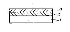
Fig. 1 is a sectional view showing a superconducting
tape in accordance with an embodiment of the present
invention; and
Fig. 2 is a sectional view showing a superconducting
wire in accordance with another embodiment of the present
invention.
DESCRIPTION OF THE PREFERRED EMBODIMENTS
~f~`.
~. . . . .
. .
132~97~
Fig. 1 iæ a sectional view showing a superconducting
tape in accordance with an embodiment of the present
invention. Referring to Fig. 1, a metal tape 1 serving
as a base material is f ir8t provided with a ceramic film
2. A film 3 of an oxide superconductor havinq perovskite
structure is-then deposited.
Fig. 2 i8 a sectional view ~howing a superconducting
wire in accordance with another embodiment of the present
invention. Referring to Fig. 2, a metal wire 11 serving
as a base material is provided on it~ outer peripheral
surface with a ceramic film 2, over which is deposited a
film 3 of an oxide superconductor having perovskite
structure.
Description i8 now made of Example6 of
~uperconducting tapes provided in accordance with the
present invention.
Example 1
Samples of superconducting tapes in accordance with
the pre~ent invention were prepared by tapes formed by
parent materials of copper with Ti film~ 1 ~m in
thickness provided on the surfaces thereof (shown a~ "1
~mTi/Cu~ in Table 1), tapes of SUS304 stainless steel and
of Cu-Ni alloy, which were provided thereon with various
ceramic films as listed in Table 1, by plasma CVD process
or ion plating. Further, thin films of Y1Ba2Cu3Ox were
formed on the tapes by sputtering. Sputtering was
performed by t (1) by heating the substrate to a
_ 9 _
.
`" 132~976
temperature of 800C; and (2) forming a film at ordinary
temperatures and performing heat treatment in the
atmosphere at a temperature of 950C.
For the purpose of comparison, thin films of oxide
superconductors similar to those of Example 1 were
respectively formed on a tape of Cu a~d those of SUS304
stainless steel directly by sputtering.
Table 1 shows properties of superconducting tapes
thus obtained.
- -- .
-- 10 --
. ~
, , : ~,, . : . . , . , .. .: . : . ~ . .
. . - ~ . ,.: -
1~26~7~
,. o o _ o -o o __ _ ~i
X oo
_ _ . _ _ _ . Ct,
I ~ I G~
_ h :~ )~ ~ h :~
~4 ~ ~ ~ U ~ .
_ n ,~ ~ ~ r~ N ~`~ ,~ Il~ ~ ul ~ ~q ~ ~ ~
E1~' ~D ~. O~ ~ ~ r,o a~ In c: ' ~ o ~ ~ t~ ,a
O ,0 O O ~0 0
_._ .__ .. _ ~ __ .~ _
~ 9
11 ~ _ _ ~~ _. _ _ _ _ ~ ,~
J O r1 _._ _ __ _ _ _~1 _ ~1 Ul
__ . _ _ _ _ h
oX h
In Ln . L
,, ,~ m ' o o _ _. ,. ,, _, N 1~ ~ ~ t~l C
C ,Up-,~ ~}
r-~ ~ _ _ _ ~ _ ::~
~ U ! j ,1~, O N~1 r ~1 ~ . \ L
~J O Lr~ _ __ __ _ _ \ ~ R
.~ \ ~
~ 1 ~ NN N ~ ~ O Z \
h t~ O~ O2 ~ 2o F~ ~ \
~ ~ ~ _ I _ ___ 1~ ~ _ _ _ _ \ .1
~ Ln 1~
~ ~1 ~ c-l . ~ ~ N ~`J N ~1 N N N O
_ o 8 8 B o __ o c o o o o . ~3
~r ~r ~ ~r ~ O u~
F~ .~ f~ ~ O O O Z 1'3 O O O h O
i= ~ ~ ~ _l O ~C
. __ 'O ,~
_ _ _ ~ Ln ~D r ~~1 r~
_ _
a~ ~ ua~a~a21 ... ~ ~
~ ~ ~ ~ o
-- 11 --
~-
132~976
From Table 1 it can be seen that the outermost film of the
superconductor had a high critical temperature while the
superconducting tape was excellent in flexibility in each -
sample prepared in accordance with the present invention.
One of the reference examples comprising a film of oxide
superconductor deposited directly on the surface of the
metal substrate, superconducted at a low critical
temperature Tc, while the remaining examples were non-
6uperconductive.
Example 2
An SiO2 film was formed on a silicon substrate by a sol-
gel method. First, water and hydrochloric acid were
added to an ethanol solution of silicon tetraethoxide to
prepare a 801 by hydrolysis. Then the silicon substrate
was dipped in this 801 to form a 801 film on the
substrate. Thereafter the silicon substrate was heated
to a temperature of 500C in the atmosphere, to cause
gelation of the sol film. Such operation was repeated
10 times, to form an SiO2 film of about 0.2 ~m in
thickness on the silicon substrate.
Samples are then prepared by forming an NgO film 0.2
~m in thickne~s and an Al203 film O.2 ~m in thickness on
the silicon substrate provided with the SiO2 film as above
by RF magnetron sputtering. Film forming conditions were
as followss
- 12 -
: . .
. . ` " ~ .
1 326976
target: NgO polycrystal or Al203 poIycrystal 100 mn
in diameter
target-substrate distance: 50 mn
~puttering ga~: Ar gas containing 10 vol.% of N2
ga6 pressure: 1 x lo-Z Torr.
output: 75 W
film forming time: 1.5 to 2 hours
It was determined by X-ray diffraction that the MgO
film thus formed had strong ~-axis orientation of ~001).
It was also determined that the Alz03 film as formed had
no uniaxial orientation.
A Y1Ba2Cu30x film 1 ~m in thickness was formed on the
MgO and Al203 ceramics films, by the sputtering method ~1)
of Example 1. A film of the oxide superconductor thus
obtained was sub~ected to measurement of zero resistance
temperature Tc and critical current density f Jc
The film of the oxide superconductor formed on the
MgO film had a zero resistance temperature Tc of 84 K and
critical current density Jc of 1000 A/cm2 at the
temperature of liquid nitrogen (77.3 K). On the other
hand, the film of the oxide superconductor formed on the
Al203 film had a zero resistance temperature Tc of 61 X.
A reference example, prepared by forming a film of an
oxide superconductor directly on a silicon substrate,
- 13 -
X
,., . . ' ' ~
. , - .:
.
, :, ::-: -.
1326976
that is, without formation of an intermediate ceramic film,
exhibited no superconductivity at the temperature of liquid
helium (4.2 K).
According to the present invention as hereinabove
described, the base material is first worked into arbitrary
configuration and size,~a first ceramic coating i8 then
formed on its surface, and a film of an oxide
superconductor i8 further formed on the same. This results
in a superconducting member having excellent properties,
formed on a substrate which may be of any desired material.
Further, the present invention can be employed in
connection with a package for a semiconductor element
formed on a ceramic substrate, as well as directly to a
semiconductor element or to a sensor with a semiconductor
substrate, to attain a very useful product. It is
difficult to form an oxide superconducting layer directly
on a metallic base material. Thus, a principal advantage
of the present invention is that it permits a product such
as a superconducting tape or a superconducting wire using a
flexible metal material as the substrate and an oxide
c~ramic as the superconductor to be formed.
Although the present invention has been described and
illustrated in detail, it is clearly understood that the
same is by way of illustration and example only and is not
- 14 -
.~ .
.
. ~ , . ~ , .
` `- 132~97~
to be taken by way of limitation, the spirit and scope of
the present invention being-limited only by the terms of
the appended claims.
- 15 -