Note: Descriptions are shown in the official language in which they were submitted.
1 327064
Phase-locked loop with circuit for adjusting a phase
comparator's output amplitude.
The present invention relates to a phase-locked loop
circuit comprising in sequential connection: a digital phase
comparator, to one input of which a reference frequency is
supplied; a loop filter; and a voltage-controlled oscillator,
from which a feedback branch is connected to the second input of
the phase comparator.
A block diagram of a phase-locked loop is shown in
Figure 1. In the figure, the reference frequency fref is applied
to the input of the phase comparator. The output of the phase
comparator is connected to the loop filter 2. The losp filter
(2) output is applied to the voltage-controlled oscillator 3.
The output of the oscillator 3 is fed back to the phase
comparator 1 so as to pro~ide a loop that is locked according to
the reference frequency fref at a certain rate~
It is well known in the art to use a phase-locked loop
in frequency synthesizers. When a phase-locked loop is used in
a frequency synthesizer, the frequency modulated voltage-
controlled oscillator (VCO~ imposes contradictory loop bandwidthrequirements. A rapid locking time is desired for channel
switching thus requiring the loop bandwidth to be as high as
possible. On the other hand, for the loop not to accentuate nor
to damp the frequency modulation, its bandwidth should be far
lower than the lowest modulation ~requency. A low loop bandwidth
also reduces the residual modulation and increases the damping
of the phase reference frequency.
t 32706~
The U.S. Pat. Nos. 4,482,869 and 4,516,083, for
instance, and EP patent application 85615 disclose an
acceleration of the loop filter by changing the resistance value
of the integrator stage of the filter by either removing
resistors or by short circuiting them. Correspondingly, the
retardation i5 achieved by removing the short-circuits or adding
resistors. In U.S. Pat. No. 4,156,855 the loop is additionally
accelerated by using a current pump to increase the current
feeding the integrator stage capacitor.
Controlling the resistors switches, however, disturbs
the operation of the loop. Thus, at the moment of switching
resistors in a slow loop, a momentary spike usually appears in
the adjusting voltage obtained from the VC0, which is
inadmissible for some applications, for example radiotelephones.
The same happens in the case of a sudden change of the current
charging the integrator.
Consequently, a frequency synthesizer formed by a
phase-locked loop has been impossible to use without drawbacks
where, a rapid locking time or a linear modulation frequency
response is requirsd. In cases where a modulated frequency
synthesizer i5 formed by a phase-locked loop there have been
compromises between the locking time, the linearity of the
modulation frequency response, and the reference frequency
damping.
For example, in radiotelephone applications requiring
a short locking time and a linear modulation frequency response,
it has been necessary to use a so-called transfer oscillator
system, in which a modulated fixed transfer oscillator frequency
--2--
1 3~706~
is mixed with the receiver in~ection frequency. On the other
hand, a transfer oscillator has the drawbacks of producing a
great number of mixing results, which are difficult to damp and
complicated and expensive circuitry.
The present invention seeks to reduce the above
problems and to provide a circuit that uses a modulated frequency
synthesizer when both a rapid locking time and a low loop
bandwidth are required.
The invention provides a phase-locked loop circuit
comprising: a digital phase comparator with a pulsed voltage
output and having a reference frequency supplied to a first
input; a loop filter which receives an output of the phase
comparator; a voltage-controlled oscillator (VCO) which receives
an output of the loop filter; a feedback branch connected from
an output of the VCO to a second input of the phase comparator;
and limiting means connected to the phase comparator for limiting
the amplitude of the pulsed voltage output of the phase
comparator so that the phase-locked loop has a modifiable
bandwidth and locking rate.
The present invention involves a modification of the
gain of a phase-locked loop by limiting the voltage of the pulses
obtained from the digital phase comparator, enabling the use of
a high bandwidth, i.e., a rapid loop during the channel switching
and a low bandwidth after the loop is locked. Since the transfer
oscillator system is not used, no detrimental mixing results are
produced.
When modifying the gain of the phase locked loop by
limiting the voltage of the pulses obtained from the digital
--3--
~, "
:
,~`
1 327064
phase comparator, the gain change does not disturb the loop's
operation.
Moreover, the circuit is simple and is appropriate for
a commonly used two-output digital phase comparator and an
operational amplifier type integrator. The circuit according to
the invention allows a stepless adjustment when desired, and the
adjustment functions flawlessly even with small phase
dif~erences.
According to the present invention, the voltage of the
pulses obtained from a digital phas~ comparator can be changed
either in or outside the phase comparator by limiting means, i.e.
by a diode, transistor, FET, or some other voltage limiting
circuit. For example, the pulse voltage limitation can be
provided either at the output of the phase comparator or of the
circuit set up before the loop filter, as described above and
shown in Figures 6a, 6b, 7a, and 7b. In the phase comparator,
the adjustment is feasible, e.g., by changing the supply voltage
of the phase comparator itself, or of its output stage.
It is essential that by changing the pulse voltage in
the circuit, the gain of the phase-locked loop can be influenced,
and thus the bandwidth, and setting time of the loop, among
- others, can be modifiedO
It is also essential that the gain change does not
disturb the loop operation by limiting the voltage of the pulses
obtained from the phase comparator. In addition, the gain is
steplessly adjustable.
Thus, it is possible to employ a high bandwidth, i.e.,
a rapid loop during the ohannel switching and reduce the loop
,, .
1 327064
bandwidth after the locking without disturbing the loop
operation.
In this way, a rapid setting time, a linear modulation
frequency response, a small residual modulation, and a great
reference frequency damping are achieved.
The circuit according to the present invention has
several phase-lock applications, such as frequency synthesis,
modulation, or demodulation applications (e.g., AM, FM, PM), a
tracking filter, the regeneration of a clock signal, and the
like.
The adjustment of a phase-locked loop gain is usable
;in various applications, e.g., adjustment of the loop bandwidth,
acceleration and retardation of the loop, linearization of the
modulation frequency response, increasing the reference frequency
damping, or, e.g., compensating the change of the loop gain as
the divisor changes.
The circuit has the additional advantages of being
simple and ~conomical, providing a controllable, and stepless
adjustment, and the gain adjustment does not disturb the loop
operation.
`~MoreoYer, the circuit is applicable to digital phase
detectors of various types, for instance single-ended output
(Figures 7a, 7b) or double-ended output (Figures 6a, 6b) phase
detectors.
Tha present application of the inv~ntion to a FM
modulated fre~uency-synthesizer is described in detail below as
an example and with reference to the enclosed drawings, in which:
_ 5 _
'
:: .
1 32706~
Figure 1 shows a block diagram of a typical phase-
locked loop;
Figure 2 shows a block diagram of a frequency
synthesizer comprising a phase-locked loop;
Figure 3 shows an embodiment of the circuit according
to the invention;
Figure 4 is a graph of pulses relating to the circuit
of Fiqure 3;
' Figures 5a and 5b are ~raphs of frequency responses
relating to the circuit of Figure 3;
Figure 6a represents a transistor limiter (Q4, Q5) set
, up outside of the digital phase comparator having double-ended
, outputs (QR, QV);
. Figure 6b represents a diode limiter (D1, D2~ set up
h,
.~ outside of the digital phase comparator having double-ended
j~ outputs (QR, QV);
.: Figure 7a represents a transistor limiter (Q6, Q7) set
up outside of the digital phase comparator having single-ended
output (Pd~; and
Figure 7b represents a diode limiter (D3, D4~ set up
outside of the digital phase comparator having single-ended
output (Pd).
~'
.~ In the frequency synthesizer of Figure 2, the reference
frequency is provided by a stable crystal oscillator 4 (TCX0).
The TCX0 output frequency is divided by the firsk divider 5 (by
the number R) in order to generate an appropriate phase
comparison frequency. The phase comparison frequency obtained
is directed to the phase comparator 1. The phase comparator
.
i -6-
:,~
`: iP~9
.
`:
1 327064
output signal is fed into the loop filter 2. This loop filter
is a low pass filter which removes the change components from the
phase comparator output signal and applies a direct-current
voltage to the control of the voltage-controlled oscillator
3(VC0~. From the output of the voltage-controlled oscillator 3,
the feedback is taken through the prescaler 8 and the second
divider 7, to the second input of the phase comparator lo The
second divider 7 of the feedback loop (divisor N) is
programmable, so that a plurality of frequencies can be
synthesized by changing the divisor N. The prescaler reduces the
frequency of the voltage-controlled oscillator 3 to the
operational range of the programmable second divider 7, the
frequency range of which usually is relatively narrow. The
output of the voltage-controlled oscillator 3 simultaneously
forms the synthesizer output frequency fout. Since this
connection is well known to a person skilled in the art, it will
not be described in detail.
.,
;~Commercially available integrated circuits comprising
i~first divider 5, the phase comparator 1 and the programmable
divider 7, are readily available and these elements are indicated
by the reference IC in Figure 2.
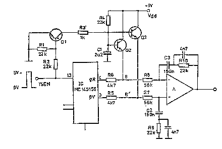
~$i,Figure 3 shows a circuit according to the present
invention, in which the above integrated circuit IC is an
MC145~56 chip (manufactured by Motorola).
This circuit includes an output phase comparator, the
outputs of which are marked hy 0V and 0R in Figure 3. These
outputs are tak~n through the resistors R5 and R6 to the
integrator, which in the embodiment shown in Figure 3 is
7--
.
1 327064
performed by differential amplifi2r A. Nevertheless, a single-
; ended output phase comparator may also be used as shown in
Figures 7a and 7b.
The natural oscillation frequency fn of the phase-
' locked loop is
0 Kvco (1)
fn~ - / -
.. 2~ ~ N C R
. . .
~, in which K0 is the gain of the phase comparator
".': 10
Kv~o i~ 2 rr-Qfvco (2)
Vvco
N is the total divisor (fou~/fref)
~ C is approx. C2=C3 in the Figure 3 and
.~ R is approx. R7-R8 in the Figure 3.
.:
.~ By changing X0
fn2 = ~ ~ fnl (3)
. .,;, ~
is obtained. In other words, the natural oscillation frequency
,i of the loop is directly proportional to the square root of the
., .~,~
.~ gain of the phase comparator~
~, In the embodiment of Figure 3, the voltage of the
' .r'
~ pulses obtained from the outputs 0V and 0R of the phase
r':
:~. comparator is influenced as follows:
After both outputs are applied to resistors R5, R6, the
~ signals are applied to the emitters of limiting transistors Q3,
-~ Q2, respectively. The collectors of the transistors (Q3, Q2) are
_~_
. ~ .
1 32706~
connected to the supply voltage Vdd (5V). In a normal situation,
a low limiting frequency (i.e., a slow loop) is switched on, with
the capacitor C1 being charged through the resistor R4 to +5V and
the transistors Q2 and Q3 limiting the 5V voltage pulses of the
outputs 0V and 0R to pulses of approx. 0.5V, as shown in Section
A of Figure 4.
At the moment of channel switching, divisor information
(i.e., a value for N) is fed into the programmable divider (e.g.,
element 7 of Figure 2) of the circuit. Simultaneously, the
activating pulse (TSEN) is fed into the terminal 13 of the
microcircuit and provides a conkrol through the resistor R2 to
the base of the switch transistor Q1. Q1 then becomes
~- momentarily conductive and the charge of the capacitor C1 is
;;~ discharged through the resistor R3. Under these circumstances,
`; the base voltage of the transistors Q2 and Q3 decreases to
approximately OV and the height of the pulses on the emitters of
the transistors rises momentarily to 5V, as illustrated in
~ Section B of Figure 4.
-i~ The increased loop gain causes the loop bandwidth to
; 20 increase. Sustaining the rapid loop, i.e., the high gain,
depends on the time constant determined by the capacitor Cl. In
the described case, the rapid loop remains switched on for
approximately 5 ms, which is enough for the loop to settle.
~ ~he natural oscillation ~requency of the described
-~ phase-locked loop with the described circuit is about 80 Hz with
`~ a rapid loop, (fnl), the natural oscillation frequency (fn2) of
'~ a slow loop is approx. 0.5/5 x 80 H~, i.e., about 25 Hz. (K01 .
Kvco/N = 2300 Hz). The set of curves of Figure 5 illustrates the
_ g _
, ~ .
1 327064
response of the locked loop of a sample circuit with a rapid loop
as well as with a slow one. From the response both the natural
oscillation frequency fn and the -3dB bandwidth of the locked
loop are readable. Moreover, the modulation frequency response
of this loop has been drawn in Figure 5 both with a rapid and a
slow loop. The modulation frequency response remains direct
within the desired range 300 Hz to lO kHz.
Figures 6a and 6b show a limiter external to the phase
comparator using transistors and diodes, respectively. The
circuit shown in Figure 6a limits the phase comparator output
through a transistor limiter. The transistor limiter includes
two transistors (Q4, ~5), each having its emitter connected to
`:
a resistor (Rll, R12). Each resistor is connected to a
respective output of the two-output phase comparator (0R, 0V).
Each transistor's collector is connectPd to the supply voltage
(+Vdd). Thus, by varying the base voltage of each transistor,
the emitter voltages will vary 50 as to regulate the output to
the loop filter.
~; Figure 6b shows a diode limiter for a two-output phase
,; 20 comparator. A first diode (D13 has its cathode connected to a
~ resistor (R13) which, in turn, is connected tc an output of the
;~ phase comparator (0R). The second diode (D2) has its cathode
~ connected to a resistor 5R14), which, in turn, is connected to
,~ the second output of the phase comparator (0V). By varying the
; voltage applied to the anodes of the diodes (Us), the diode
outputs regulate the output applied to the loop filter.
Figures 7a and 7b show limiting circuits for limiting
the output o~ a one-output phase comparator. Figure 7a shows a
~'~
~ -~ 0-
.
.,
-- 1 327064
transistor limiter having two emitter coupled transistors,
wherein the emitters are both connected to a resistor (R15),
which, in turn, is connected to the output (Pd) of the phase
comparator. One transistor (Q6) is an NPN transistor having its
collector connected to the supply voltage (+Vdd), and a second
PNP transistor (Q7) has its collector connected to ground. Thus,
by varying the voltage applied to the base of each transistor
(Ua, Ub), the emitter voltages of the transistors are varied,
thus modifying the voltage supplied to the loop filter.
... .
Figure 7b shows a diode limiter controlling a one-
output phase comparator. This circuit comprises two diodes (D3,
D4). The first diode tD3) has its cathode connected to the anode
of the second diode (D4) and a resistor (R16). The resistor is
connected to the output Pd of the phase comparator. By
regulating the voltage applied to the anode of D3 (Ua) and the
cathode of D4 (Ub), the output sent to the loop filter may be
adjusted. - /
,,~ /
;; /
i~,`~ /
~ /
~`''~' /
~: /
~ /
r ~
7~
.
.,