Note: Descriptions are shown in the official language in which they were submitted.
;~
~ 1327~0~
. .
~.
- POINT OF SALE REGISTER SYSTEM
..,
S Fleld of the Invention
- The invention relates to a point of sale register
system utilizing a plurality of point of sale registers,
also referred to as cash registers, and more particularly,
to a point of sale register system having an improved
.
' capability to manipulate data.
:;
Description of the Back~round Art
~; Previously, many retail operations have utilized a
plurality of point of sale registers, each coupled to a
central computer. Each of the registers contain a processor
and are coupled to one of a plurality of optical character
readers, or OCR's. Each of the OCR's scan alphanumeric
prsduct identification information from products to be
purchased and transfer this scanned information to its
respective register.
, The central computer stores information correlat-
ing the product identification information for each of the
- products to the product's specific sales price. The regis-
ter communicates with the central computer to obtain the
- specific price of each item scanned. This eliminates a
requirement to individually key into the register the price
of each item purchased. However, while most products
^~ include a standard bar code encoded product identifier
placed on the product by the manufacturer, alphanumeric
product information must be added for each specific item by
the particular retail operation.
' ''
. "~, I .
. .
''',''~
".. , :~
,'~ ~, .
,:,
~.:
- .
:
` ``" - 2 - 1 32740~
..,..
?~
" . .
Often the purchases are charged on a credit card.
The central computer fur~her contains information regarding
an account status of each outstanding credit card account.
If the credit card is o equipped, the OCR scans an alpha-
~5 numeric account number representation from the credit card.
:.
;In this manner, the information can be transferred to the
` central computer to determine the account status of that
particular credit account.
, .. .
If the central computer determines that no addi-
tional credit is to be allowed, and the purchaser still
desires to make the purchase by credit card, a phone call is
-manually initiated to a human operator who has authority to
override the central computer. The store clerk must first
inform the operator of the particular credit account number
and the amount of additional credit desired, as by utilizing
~ ,.. . .
the touch-tone pad of the telephone. However, it is gener-
.... .
~ally recognized by those skilled in the art a~ an inherent
.
problem that this form of data entry often results in
~`errors, requiring time consuming reentry of the information
, . . - .
by the store clerk.
Many credit cards are provided with a magnetic
~!stripe onto which data, such a~ its respective credit
account number and expiration date, i8 stored. The data
stored on the magnetic stripe of such credit cards is
'i 25 scanned by moving the magnetic stripe past a magnetic head
o~ a magnetlc stripe reader which reads the data. However,
registers have been incapable of receiving and utilizing
~this data. Further, the card has been capab1e of being
-passed by the magnetic head in only one, predetermined
--~ 30 direction, referred to as a forward scan, but ~uch
,~
~, q .
, ,
, ' ' .
.,
,.",
"~, ,
... . . . .. .
. ~, . ,,, ,. _ __ _ , , . _ . . _. _
. .
. .
'~` ~ 3 ~ 1327~0~
"unidirectional scanning" often makes it physically awkward
to scan the credit card.
Another limiting feature of point of sale register
` systems is that standard microprocessors typically have a
~ 5 single input/output (or I/O) port. Thus, when it has been
- desirable for the microprocessor to communicate with a
plurality of peripheral devices, complex circuitry has been
required.
The invention disclosed herein is provided to
overcome some or all of the above problems.
Summary of the Invention
Accordingly, applicants' invention seeks to provide
a point of sale register system.
- . .
Further, applicants' invention seeks to provide an
interface circuit for a point of sale register which
facilitates a transfer of data between the point of sale
register and any of a plurality of peripheral devices coupled
thereto.
In accordance with the invention, the peripheral
devices can by way of example include a bar code reader, a
magnetic stripe reader, a telephone, a printer or any other
similar device.
- Still further, applicants' invention seeks to
provide an interface circuit which can interpret data scanned
by a reader from a magnetic stripe of a credit card
regardless of whether such data was so scanned by the reader
in a forward or a reverse direction.
Further still, the invention seeks to provide a
circuit which will allow a microprocessor having a single
;. .,
f~ 30 serial I/O port to selectively communicate with any of a
plurality of serial devices, such as the peripheral devices
~; coupled to the interface circuit.
", ,
lB
;,
; ;. , :
~ .
, " : :
~`
1327~0~
- 4 -
The invention in one broadly claimed aspect provides
a circuit for permitting a processor having a single serial I/0
port comprising a transmit channel and a receive channel to
communicate with a plurality of peripheral devices each having
serial I/0 ports comprising a transmit channel and a receive
~- channel. The circuit comprises first means for determining
which of the peripheral devices has data to be transferred to
the processor, second means for determining to which of the
peripheral devices the processor has data to be transferred and
third means responsive to the first and second determining means
` for determining which of the data is to be transferred. There
,.: ,'
, is provided switching means comprising first means for
selectively coupling the transmit channel of the processor to
.j
- the receive channel of each of the peripheral devices and second
means for selectively coupling the receive channel of the
., 1,
processor to the transmit channel of each of the peripheral
~ devices, the switching means being responsive to the third
,`~'?i determining means for controlling the first and second
"
- determining means to permit transfer of the data.
......
The invention in another aspect pertains to a point of
sale terminal for implementing customer transactions and
~ including a point of sale register having a processor with a
; single input/output (I/0) port, an interface circuit for
~ facilitating transfer of customer transaction data messages
-.
between the point of sale register and a peripheral device, the
data messages comprising a plurality of sequential characters of
;~i data related to a customer transaction. The interface circuit
comprises electronic circuit memory means for providing
temporary storage of characters of data to be transferred
between the register and the peripheral device, first data
transferring means operatively coupled between the register
single I/0 port and the electronic circuit memory means for
., ~
:~
` 13274~
-~ - 4A -
transferring characters of data between the register and the
electronic circuit memory means and second data transferring
- means operatively coupled between the electronic circuit memory
means and the peripheral device for transferring characters of
~ 5 data between the electronic circuit memory means and the
- peripheral device. Message determining means determines if a
- complete customer transaction data message has been received by
the electronic circuit memory means and a programmed processing
circuit including a programmed microprocessor operates a control
means operatively coupled to the first and second data
transferring means and the message determining means for
; controlling the first and the second data transferring means to
begin transferring characters of data for a selected customer
transaction data message from the electronic circuit memory
means to one of the register or peripheral device virtually
immediately after the message determining means determines that
a complete data message has been received from the other of the
register or peripheral device.
;:. In the embodiment disclosed herein, the interface
.. ~
circuit is coupled to an NCR 2152 cash register, sold by the NCR
- Corporation of Dayton, Ohio. However, this particular point of
; sale register is for description only and should not be
construed as a limitation of applicants' invention.
In a preferred embodiment, a register system for
facilitating point of sale transactions of any of a plurality of
.~
~,~ products is provided, wherein each of the transacted products
.~i have a bar code encoded product identification associated
:~ therewith. The register system comprises a central processor,
~- means associated with the central processor for storing data
representing a sales price for each of the products and a
plurality of distributed point of sale registers coupled to the
central computer. The register system further comprises a
~' .
.
,
13274~
- - 4B -
.
plurality of bar code readers, wherein one of the bar code
5, readers is associated with each of the registers, each of the
bar code readers for scanning the bar code encoded product
identification from the transacted product and means responsive
. 5 to the scanned bar code encoded product identification and the
. stored product information for transferring to the register
. i
~ associated with the bar code reader the product sales price for
..
;; the product scanned.
r Yet further, the present invention also seeks
~: .
~ `
; .~,
~,:..~
.; .
:;
.
, ....
.,, ~ .
~,,.?~
..~
, . *
:'.
. ."~ .
. ~, .
,`.' 1
, ~
' ,~
., .
,"
, ,. . .'
-: ~
""
, ~"
' :,
'`' ~
'''
' ' :
- ~ 5 ~ 13274~
to provide a bidirectional card reader for reading data
stored on a magnetic stripe on a card as a sequence of
multi-bit characters of the same bit length. The
bidirectional card reader comprises a scanning head, means
for sequentially reading the data bit-by-bit as the card is
passed relative to the scanning head, means for sequentially
storing the bits as the bits are scanned, means for deter-
mining whether the card was passed by the scanning head in a
forward or a reverse direction, means for locating the last
data bit received if the determining means determines that
the card was passed in the reverse direction and means
responsive to the locating means for correctly grouping the
stored bits as the multi-bit characters ctored on the
.
magnetic stripe.
Still more particularly, the present invention
seeks to provide a circuit. for permitting a processor
having a single serial I/0 port including a transmit channel
and a receive channel to communicate with a plurality of
.~ peripheral devices each having serial ~/0 ports including a
transmit channel and a receive channel. The circuit com-
r prises first means for determining which of the peripheral
.
~: devices has data to be transferred to the processor, second
- means for determining to which of the peripheral devices the
.. processor has data to be trans~erred, third means responsive
to the first and second determining means for determining
which of the data is to be transferred and switching means
comprising first means for selectively coupling the transmit
. channel of the processor to the receive channel of each of
the peripheral devices and second means for selectively
coupling the receive channel of the processor to the trans-
. mit channel o~ each o~ the peripheral devices, the switching
means being responsive to the third determining means for
. . .
, ," .
~,
~ 6 - 1327~
,
controlling the first and second determining means to permit
transfer of the data.
Other features and embodiments of the invention
i will be apparent from the following specification taken in
conjunction with the accompanying drawings.
, i
Brief Descri~tion of the Drawinas
Fig. 1 is a block diagram of a point of sale
" '!
'( register system according to the present invention:
~, F~g. 2 illustrates a product to be sold including
10 a bar code;
Fig. 3 illustrates a credit card including a
magnetic stripe;
' Fig. 4 is a block diagram of an interface board
according to the present invention;
...
~' 15 Flgs. 5-13 are flow charts illustrating operation
- of the interface board according to the present invention:
Fig. 14 is a graphic illustration o~ data stored
on the magnetic stripe of the credit card of Fig. 3;
...
:Fig. 15 is a chart illustrating an ANSI standard
: .
~20 X4.16 digital representation of characters stored on the
,:,
magnetic stripe of the credit card of Fig. 3;
Fig. 16 is an isometric view of a credit card
reader; and
Fig. 17 is a graphic illustration of a micropro-
25 cessor accumulator.
... .
Descriptlon of the Preferred Embodiment
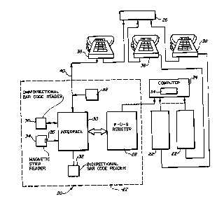
- According to the present invention, a point of
~-sale register system 20 which includes a plurality of point
' .
,
,
, 1327~0
.,
-~ of sale terminals 22, a central co~puter 24 and a voice
; com~unication device 26 is illustrated in Fig. 1. Each of
the point of sale terminals 22 is coupled to peripheral
devices including a polnt of sale register 28, an interface
board 30, a bidirectional bar code reader 32, a magnetic
stripe reader 34, an omni-directional bar code reader 36 and
a telephone 3 8 . By way of example, the register 28 can be
an NCR 2152 terminal, manufactured by NCR Corporation of
~ Dayton, Ohio, or any other processor based register.
- 10 As for the other peripheral devices, the omni-
directional bar code reader 36 can be of a type such as, for
example, the one manufactured by I3M Corporation. The
bidirectional bar code reader 32 can be of a type such as~
for example, the HP 6300 series contact wand a~ distributed
by Hewlett Packard, 350 West Trimble Road, San Jose, Cali-
r~;' fornia 95131, the Laserscan 7000II hand held scanner,
~ distributed by Symbol Technologies, Inc., 1101 Lakeland
j.l
-~ ~venue, Bohemia, New Yor~ 11716, or other such devices well
known in the art. Further, the magnetic stripe reader 34
can be of a type such as, for example, the MT-211 card
",
~ reader distributed by MAGTEK of 20725 South Annalee Avenue,
., .
Carson, California 90746 and include~ a magnetic stripe
reader head 37.
As will be understood by referring to Fig. 1, the
~: .
register 28 couples the point of sale terminal 22 to the
central comp~ter 24. The bidirectional bar code reader 32,
the magnetic stripe reader 34 and the omni-directional bar
code reader 36 are then coupled to the register 28 by the
interface board 30. Finally, the telephone 38 and the
.,
''' .
, . . --- ,
~ 8 1327~
.;
interface board 30 are mutually coupled in parallel to the
voice communication device 26 by a telephone line 40.
While not limited as to application, the point of
` sale register system 20 is designed for utilization in large
5 retail operations. Typically, such retail operations have
many departments, wherein at least one point of sale termi-
~-!
nal 22 is located in each of the departments for selling a
product 42, as for example a shirt, as illustrated in Fig.
. .,
j 2. As shown, the product 42 includes a tag 44 having a
preprinted bar code representation 46 thereon which identi-
~; fies the product 42.
,
By way of example, the bar code representation 46
may be in any bar code format now known or subsequently
, . ~
q developed, including but not limited to Code 39 (3 of 9),
' '1
; 15 Code 128, and UPC Code.
....
, As illustrated in Fig. 3, a credit card 48 typi-
- cally includes a magnetic stripe 50 onto which data is
stored. Specifically, the credit card 48 is associated with
a specific credit account having a specific credit account
.
20 number and the magnetic stripe 50 includes first, second and
~- third data tracks 52a, 52b and 52c, onto which three tracks
of data are stored, directed from left to right with respect
~ to Fig. 3. As described in greater detail below, the credit
;- account number is encoded on the second data track 52b as
` 25 credit account number data.
Referring again to Fig. 1, the central computer 24
includes a central computer memory 54 which stores price
information for every product sold by the retail operation.
Thus, for example, when a customer desires to purchase the
30 product 42 (Flg. 2), the bar code representation 46 on the
, .
. .
-- -9- l327~a~ '
tag 44 is scanned by either the bidirectional bar code
reader 32 or the omni-directional bar code reader 36. After
the tag 44 has been scanned, the information is received by
~ the interface board 30 and transferred to the register 28.
i The register 28 then accQsses the central computer
memory 54 of the central computer 24 to determine the sales
price of the product 42 selected by the customer for pur-
; chase. This is done for each product to be purchased. The
register 28 then sums the individual sales prices of each of
- 10 the products to be purchased and calculates a total sales
i~ , .
price, upon which applicable sales tax or other charges are
added.
'
;If the purchase is to be by cash, the customer
simply pays cash. However, the purchase may be charged on
the cred~t card 48. The credit card 48 may be either one
issued by the particular retail operation, or a bank or
other card.
If the purchase is to be charged on the credit
card 48, the magnetic stripe 50 is passed by the magnetic
2Q stripe reader head 37 of the magnetic stripe reader 34. The
magnetic stripe reader 34 reads the credit account number
data from the second data track 52b. As is described in
greater detail below, the credit card 48 can be passed by
the head 37 of the magnetic stripe reader 34 in either
25 direction.
The interface board 30 receives the credit account
nu~ber data read by the magnetic stripe reader 34 and
transfers this data to the register 28. The ~entral com-
puter memory 54 further includes information indicating an
30 account status of each of the credit accounts (i.e., whether
o- 13274~
additional credit purchases are to be allowed on any parti-
' cular credit account). The register 28 accesses the central
computer memory 54 to determine the account status of the
credit account for the credit card 48 just scanned.
~^ 5If the central computer memory 54 indicates that
additional credit is to be allowed, the register 28 proceeds
`- to charge the particular credit account with the total price
of the purchase. However, if the central computer memory 54
determines that additional credit is not to be allowed, the
register 28 displays this information to the sales clerk.
I~ the customer still wants to charge the purchase to their
credit account, the interface board 30 automatically dials a
predetermined telephone number to connect the telephone 38
with the voice communication device 26 of a central credit
department.
At that point, the customer can explain to the
credit department why additional credit should be allowed,
after which the credit department may chose or decline to
authorize additional credit. To expedite such authoriza-
tion, the interface board 30 can further transmit informa-
tion to the credit department identifying the particular
credit account in question and the amount of additional
credit desired.
The interface board 30 is illustrated in block
diagram in Fig. 4 and includes a processor 55, including
on-board random access memory (RAN) 55a, which can by way of
example be an Intel 8031 microprocessor. The processor 55
performs primary control over the interface board 30 and
controls data flow between the register 28 and the peri-
30 pheral devices.
. , .
,,
327~0~,
.~.
The interface board 30 further includes an inter-
rupt logic device 56, an address decoder and control logic
device 58, a buffer status device 60, an input character
buffer device 62 and an output character buffer device 64 to
. ~,
facilitate transfer of data between the processor 55 and the
-register 28, as described in greater detail below.
To connect to, and automatically dial, the tele-
.~
phone 38, the interface board 30 includes a dialer device
66, a telephone coupler device 68, a line switch device 70
:.
and a telephone jack 72. The dialer device 66 generates a
touch-tone signal under control of the processor 55, the
telephone coupler device 68 provides isolation between the
, ;.j
;interface board 30 and the telephone line 40 and the line
switch 70 makes and breaks the connection between the
; 15 telephone coupler device 68 and the telephone line 40. As
for the telephone jack 72, it is preferably a standard
modular telephone connector which allows the telephone 38 to
removably connect with the interface board 30.
Still referring to the block diagram as illustra-
ted in Fig. 4, the interface board 30 further includes a
buffer device 74 which couples the magnetic stripe reader 34
, ,
to the processor 55 in a manner providing signal buffering.
More specifically, the buffer device 74 provides signal
buffering between the magnetic stripe reader 34 and the
processor.55 to protect the processor 55 against potentially
.damaging electrostatic discharge generated by the magnetic
stripe reader 34.
The processor 55 has a single serial channel 75 to
which transmit and receive data lines 76, 78, respectively,
, ~,
; 30 are coupled. The interface board 30, however, has first,
. ,'
: -,
~ ~ .
~12 - 1327~6
''''
~second and third serial ports 80, 82, 84 respectively. To
,...
permit the serial channel 75 of the processor 55 to selec-
tively communicate with devices coupled to any one of tha
~ three serial ports 80, 82, 84, an I/O interrupt logic device
;`~5 85, an I/O device selector 86, a transmit channel selector
device 87 and a receive channel selector device 88 are
provided.
Each of the serial ports 80, 82, 84 are coupled
both to the transmit channel selector device 87 and the
receive channel selector device 88, and to the I/O interrupt
logic device 85. When one of the serial ports 80, 82, 84
has data for the interface board 30, the particular serial
port 80, 82 or 84 addresses the I/O interrupt logic device
85 to inform the interface board 30 that such serial port
~.,
80, 82 or 84 has data therefor. The I/O interrupt logic
;~device 85 commands the I/O device selector 86 under control
. .
of the processor 55 to couple the receive channel selector
device 88 to the one of the serial ports 80, 82 or 84 having
such data and the receive channel selector 88 passes the
20 received data to the processor 55 via the receive serial
~'data line 78. Similarly when the processor 55 has data to
. .................................................................... .
output to one of the serial ports 80, 82 or 84, the pro-
- cessor 55 commands the I/O device selector 86 to couple the
;- transmit channel selector device 87 to the desired one of
; 25 the serial ports 80, 82 or 84. Thus, the transmit channel
~ selector device 87 and the receive channel selector device
,~ 88 each operate effect~vely as three position switches to
selectively couple any one of the serial ports 80, 82 or 84
with the processor 55 upon command from the I/O device
'''
'
'
~ , .
,' ~ ' ,
~ 13 - 1327~6
~.
selector 88. This transfer of data is described in greater
detail below with respect to the flow charts of Figs. 5-13.
~;^ In the embodiment described herein, the bar code
reader 32 is coupled to a decoder 93 and to the serial
','J 5 channel 75 of the processor via the transmit channel selec-, ,, : .
tor device 87 and the receive channel selector device 88.
Specifically the decoder 93 is the HBCR 2000 Multi-Purpose
Bar Code Decoder IC manufactured by Hewlett Packard Bar Code
; Products, 350 West Trimble Road, San Jose, California 95131.
As is well known in the art, an address latch 93a and rando~
.~
access memory 93b are each coupled to the decoder 93. A
more detailed description of the HBC~ 2000 Multi-Purpose Bar
Code Decoder IC is found in Hewlett Packard Manual Part No.
~ 5954-2165, dated January 1986 and distributed by Hewlett
i'~ 15 Packard Bar Code Products.
~i The bar code representations 46 (Fig. 2) can, for
,..."~
~ example, be encoded in any of five presently known standard
,.,: .
bar code types. The decoder 93 will decode any of the five
different bar code types, transmitting the resultingly
20 decoded data to the processor 55 via the receive channel
selector 88 and the receive serial data line 78. However,
the specific embodiment described herein for purposes of
.
- illustrating the invention utilizes only Code 3 of 9, UPC
Code and Code 128.
The interface board 30 further includes second
random access memory (RAN) 94, read only memory (ROM) 95, an
I/O decoder device 96 and a control logic device 98. The
ROM 95 store~ an operating program for the processor 55, and
the second RAM 94 provides temporary storage for data
30 passing between the peripheral devices and the register 28.
.`
,
.
:
- 14 - 132 7~ ~ ~
The I/0 decoder device 96 selects the particular peripheral
device to be addressed by the processor 55, and the control t
:~- logic device 98 provides handshaking and control signals
necessary for the processor 55 to acce~s various logic
blocks. Specifically, the control logic device 98 enables
- the processor 55 to view one peripheral device at a time and
the interrupt logic device 56 informs the register 28 when
`~ the interface board 30 has data to transmit to the register
.~i 28. ~rd
,, .~
~`- 10 The address decoder and control logic device 58
provides necessary handshaking signals required for data
: , . . .
. interchange between the interface board 30 and the register
28. The input character buffer device 62 stores one charac-
ter of data at a time as data is transferred from the
~ 15 register 28 to the interface board 30. Similarly, the
.. output character buffer device 64 stores data one character
at a time as data is transferred from the interface board 30
to the register 28. The buffer status device 60 allows both
. ~ ,. .
:~- the register 28 and the interface board 30 to monitor the
.,, ., 1
i~ 20 status of data in either the input character buffer device
., ,
~ 62 or the output character buffer device 64. Specifically,
the buffer status device 60 tells the interface board 30 if
a character is currently in the input character buffer
. device 62 and tells the register 28 if a character is
currently in the output character buffer device 64.
The interface board further includes an address
.~ latch device 100 and a bidirectional data-bus driver device
102. Data is transferred as two segments, the first segment
. .
containing its intended address and the second segment
0 containing its message. The address latch device 100 stores
~'~
.
.,
.,,
^~
~- - 15 - 1 32740~
,`. ~:
the addres~ segment enabling the intended device to receive
or transmit the message segment. The bidirectional data-~us
driver 102 controls the direction o~ data flow to the
. .
~` processor 55.
; 5 Figs. 5-13 co~bine to form a flow chart to illu8-
', trate operation of the interface board 30.
Operation begins in a first block 110 (Fig. 5)
,~1 upon application of power to the interface board 30.
Following power up, control passes to a block 112 which
~$;ii~ 10 performs a checkerboard test o~ the on-boi~rd RAM 55a resi-
dent on the processor 55. The checkerboard test is per-
, formed by first writing zeros and ones alternately in memory
'I locations o~ the on-board RAM 5Sa and then reading these
locations to confirm that the zeros and ones are correctly
in their respective locations. The checkerboard test
~i con~inues by subsequently alternately writing zeros and
~; ones, but reversing their locations. These memory locations
i are again read to confirm their correct values. Upon
~1~ completion o~ the checkerboard test, control passes to a
`il 20 block 113 which determines whether the checkerboard test was
., passed.
j I~ the test was not passed, control passes ~irst
to a block 115 which disables the interface board 30 and
, subsequently to a block 116 which commands the register 28
25 to display an error message. The register 28 continues to
display the error message until manually cleared. However,
if the checkerboard test is passed, control passes to a
block 118 which performs a similar checkerboard.test on the
second RAM 94.
.'~ .
- . ., , ~.
" , . : .
- 16 - 1 32 740 ~
Upon completion of the checkerboard test on the
second RAM 94, control passes to a block 120 which deter-
mines whether this test was pas~ed. If the block 120
--, determines that the second RAM 94 checkerboard test was not
passed, control passes to the block 115. If the block 120
~! determine~ that the second RAM 94 checkerboard test was
passed, control passe~ to a block 122 which determines
whether the decoder 93 is operational. The HBCR-2000
! decoder of this preferred embodiment performs its own
diagnostic routine, so the block 122 simply addresses the
decoder 93 to determine whether the decoder 93 passed its
diagnostic routine. If the deccder 93 does not pass its
diagnostic routine, control passes to the block 115. If the
decoder 93 does pass its diagnostic routine, control passes
to a block 124 which commands the register 28 to proceed
after which control passes to a block 126, Fig. 6.
The block 126 initializes all operation parameters
to their starting conditions, and control then passes to a
block 128. The block 128 addresses the buffer status device
60 to determine whether there is data to be transferred
between the register 28 and the interface board 30. If
there i8 such data, control passes to a block 130 which
dete~mines whether this data is to be transferred from the
register 28 to the interface board 30, or vice versa.
If the data is to be transferred from the register
28 to the interface board 30, control passes to a block 132,
Fig. 7. If the data is to go from the interface board 30 to
the register 28, control passes to a block 134, Fig. 13.
. ~ ~
Referring ayain to the block 128, Fig. 6, if there
is no data to be transferred between the register 28 and the
' '
.
,
:~ - 17 - 132740
.`
interface board 30, control pa88e8 to a block 136 which
; det~rmines whether a strobe signal is being received from
the magnetic strip~ reader 34 (see Fig. 4), which is more
; specifically illustrated in Fig. 16. The magnetic stripe
S reader 34 includeQ a longitudinal groove 137 ad~acent the
magnetic stripe reader head 37. The credit card 48 is drawn
~;;
through the groove 137 with the magnetic strip~ 50 ad~acent
to and directed toward the magnetic stripe reader head 37.
' I /! The credit card 48 can be drawn past the magnetic stripe
reader head 37 in either a forward direction or in a r~verse
direction. As the magnetic stripe So i8 drawn past the
magnetic stripe reader head 37, data stored on the magnetic
:,
stripe 50 is read by the magnetic stripe reader head 37.
The magnetic stripe reader 34 generates three
signals, as illustrated in Fig. 14 as curves 14a, b and c.
The ~irst signal is a card present signal (14a), which is
zero except when the credit card 48 is placed within the
groove 137. The second signal is a strobe signal (14c),
which is a square wave stored on the magnetic stripe 50 and
which ha~ a frequency proportional to the speed at which the
credit card 48 is drawn past the magnetic stripe reader head
. :j . .
37. The third signal is a data signal (14b) representing
the actual data stored on the second track 52b o~ the
- magnetic stripe 50.
; 25 Referring again to Fig. 6, if the block 136
determines that the strobe signal is present, indicating the
credit card 48 is in the groove 137 of the magnetic stripe
reader 34, control passes to a block 139, Flg. 9. I~ the
block 136 determines that th~ strobe signal is not present,
30 control passes to a block 140 which polls the I/0 interrupt
:.
.: .
` ~ - 18 - 132740~
'.'
logic device 85 to determine whether the decoder 93 has
,
data. If the block 140 determines that the decoder 93 does
have data, control passes to a block 142 of Fig. 12. If the
block 140 determines that the decoder 93 does not have data,
control passes to a block 144 which polls the I/0 interrupt
logic device 86 to determine whether the second serial port
82 has data.
, If the block 144 determine~ that the second serial
port 82 has data, control passes to the block 142, Fig. 12.
If the block 144 determineQ that the second serial port 82
does not have data, control passes to a block 146 which
polls the I/0 interrupt logic device 86 to determine whether
the third serial port 84 has data. I~ the third serial port
84 has data, control passes to the block 142, Fig. 12. If
the th~rd serial port 84 does not have data, control returns
to the block 128.
. ' Thu8, the control loop comprising the blocks 128,
136, 140, 144 and 146 causes the processor 55 to sequen-
tially determine whether data is to be transferred between
the register 28 and the interface board 30, whether the
credit card 48 is being scanned, whether the bar code reader
is being utilized, whether the omni-directional bar code
reader 36 is being utilized and finally whether some data is
to be received via the third serial port 84.
A~ indicated above, if the block 130 determines
that there is data to be transferred from the register 28 to
the interface board 30, control passes to the block 132,
Fig. 7. The data to be transferred from the register 28 to
" the interface board 30 is actually for one of the peripheral
devices. The data forms a message comprising a plurality of
.
,
~.,,
~ - lg - 1327~0~ ~
seguential characters, the first character indicating the
particular peripheral device intended followed by text
characters and terminating with an "end of message" charac-
f` ter.
;-~ 5 The blocX 132 reads the buffer status device 60,
and control passes to a block 152. The input character
: buffer device 62 receives characters, one at a time, from
the register 28, and the buffer status device 60 monitors
whether the input character buffer device 62 has received a
~ 10 character. The block 152 determines whether a character has
been received by the input character bufSer device 62 and,
i~ not, control returns to the block 148, Fig. 6. However,
control passes to a block 154 in the event that the block
152 determines that a character has been received by the
input character buffer device 62, and the block 154 reads
the character stored in the input character buffer 62 and
. .,
~, stores the character in the second RAN 94. Control then
'i
passes to a block 156.
When thls occurs, the block 156 looks at the
'- ~
character just read by the block 154 to determine whether
;l the character was the "end of message" character. If the
block 156 determines that the character was not the "end of
mes6agQ" character, control passes to the block 148, Fig. 6.
If the block 156 determines that the character was
the "end of message" character, con~rol passes to a block
158. The block 158 retrieves the first character of the
message stored in the second RAM 94 by the block 154. The
first character indicates the intended peripheral device for
the message, and control then passes to a block 160. The
block 160 determines whether the message is for the omni-
' ''
.''''
,
;,
, .
i,. ..
,' - ': - '
. ~
1327~0~ ~
directional bar code reader 36 (via the second serial port
82). If so, control passes to a block 162 which transmits
the message to the second serial port 82, and control
returns to the block 126 of Fig. 6.
If the block 160 determines that the message is
, not for the second serial port 82, control passes to a block
164, which determines whether the message is for a peri-
pheral connected to the third serial port 84. If so,
control passes to a blocX 166 which causes the message to be
transferred to the peripheral via the third port 84, and
control then returns to the block 126, Fig. 6.
If the block 164 determines that the message is
not for the third serial port 84, control passes to a block
.,
-~: 168 which determines whether the message is for the bar code
. `1
- 15 reader 32 via the first serial port 80. If so, control
passes to a block 170 which transmits the message via the
first serial port 80 to the bar code reader 32, and control
subsequently returns to the block 126 (Fig. 6).
If the block 168 determines that the message is
not for the bar code reader 32, control passes to a block
. .t
172 which determines whether the message is for setting the
~,.,! edit parameters of the magnetic stripe reader 34. If so,
control passes to a block 174 which checks for syntax of the
.. .
message. The register system is provided to accept credit
cards issued from only certain predetermined institutions.
~ Thus, the block 176 presets the type of allowable credit
-,~ cards 48 to be accepted at the register 28.
If the message is not for editing the data from
; the magnetic stripe reader 34, control passes to a block 178
which determines whether the message is for the dialer
,'~ .
.'~ .
,
,:,^ . ,
,
.,1 ~'
- 21 -
13274~ ~
device 66. If so, control passes to a block 180, Fig. 8.
If the message is determined not to be for the dialer device
66, and thus not for any of the peripheral devices, control
passes to a block 182, Fig. 8.
As indicated above, if the block 178 determines
- that the message received from the register 28 is for the
~1 .
I dialer device 66, control passQs to the block 180, Fig. 8.
I~ the message is for the dialer device 66, the characters
following the first, identifying character of the message,
`10 should represent legitimate digits to be dialed by the
dialer device 66 (i.e., the numbers 0-9 the "*" key and the
"#" key), and the block 180 will view these characters to
determine whether they in fact are legitimate digits to be
-~dialed. If they are not, control passes to the block 182
which commands an error message to be written to the output
character buffer 64, and control passes to a block 184, Fig.
13.
.,
.
I~ the block 180 determines that the characters do
in fact represent legitimate digits to be dialed, control
; 20 passes to a block 186~ Th~s activates the line switch 70
placing the telephone line 40 (Flg. 2) in an off-hook
condition. Control then passes to a block 188 which causes
a ten millisecond delay. This allows stabilization of the
telephone line 40, at which time control passes to a block
25 190. The block 190 causes the dialer device 66 to sequen-
, .
; tially dial the telephone number and, upon completion of the
dialing, control passes to a block 192.
The block 192 causes the line switch ~70 to go in
an on-hook condition, disconnecting the dialer device 66
0 from the telephone lin~ 40. It is to be understood that
'
.... ......... . . . . .
- 22 - 1 3 2 7~ 0~
., .
prior to the automatic dialing, the sales clerk would have
manually lifted the receiver of the telephone 38. Thus, the
dialer device 66 simply dials a predetermined number for the
operator. However, when the line switch 70 disconnects the
- 5 dialer device 66 from the telephone line 40, the telephone
38 remains connected because its receiver is still off-hook.
After the block 192 has caused the line switch 70
to disconnect the dialer device 66 from the telephone line
40, control pas6es to the block 126, Flg. 6.
~ 10Returning to Fig. 6, as discussed previously, if
; the block 136 determines that a strobe pulse is not present,
control passes to the block 140. However, if the block 136
determines the presence of a strobe pulse, control passes to
the block 139, Fig. 9.
15As discussed above, the credit account number of
the credit card 48 is stored on the second data track 52b of
the credit card 48. The credit account number comprises a
:i,..
plurality of characters, each character sequentially stored
on the second track 52b as a five bit character. Fig. 15
`~ 20 illustrates the American National Standards Institute (ANSI)
: ,`
l standard X4.16 coding. Specifically, four bits B3, B2, Bl,
;~ B0 are text, and the f ifth bit is an odd parity bit P. The
five bit character is actually stored on the second track
52b beginning with B0 and ending with the parity bit P.
- 25 This is so the bits B0-B3 are received first, and a parity
bit is computed to then be compared to the received parity
bit, as is well known in the art.
.... .
Fig. 14 illustrates the three output signals
generated by the magnetic stripe reader 34.
.. .
.'', '.
.,
:: .
- 23 - 1 ~2 7~ ~ ~
.
- As discussed above, the credit card 48 can be
drawn through the groove 137 in either direction (i.e., a
forward scan or a reverse scan). However, the data is
encoded on the magnetic stripe 50 in only the forward scan
direction. Thus, the immediately following discussion is
with re~pect to a forward scan, and it will be discussed
later how to effect a reverse scan.
Initially each of the output signals are zero.
.i'
When the credit card 48 is inserted in the groove 137, the
card present signal (14a) changes states from zero to one.
The card present signal remains high until the credit card
48 is removed from the groove 137.
As the credit card 48 is drawn through the groove
137, the magnetic stripe reader 34 reads a square wave
comprising alternating zeros and ones from the magnetic
~ stripe 50 and generates a strobe signal (Fig. 14c). The
: frequency of the strobe signal is dependent upon the speed
at which the credit card 48 is drawn through the groove 137.
The strobe signal provides timing for decoding the data
` 20 signal, discussed below. The data is not stored on the
: second data track 52b along the entire length of the credit
card 48, but rather is centered. Thus the data signal does
not begin concurrent with the strobe signal, but rather
after a certain distance along the magnetic stripe.
The data i stored on the second track 52b in the
order of first a start character, then at least one text
.
character. Then there is a stop character followed by a
longitudinal redundancy check, or LRC, character. Referring
to Flg. 15, from B0-P, the start character comprises the bit
30 pattern 11010 and the stop character comprises 11111.
,..
` ^- 24 - 1327~6
Referring again to Fig. 14, and viewing the data
signal 14b fro~ left to right, the data signal remains low
until bit B0 of the start character is received. As is dis-
. . .
cussed in greater detail below, this transition from o to 1
of the data signal 14b indicate~ the beginning of the datasignal. Following the textual data is the stop character
:`
which, as indicated above, comprises the characters 11111
.,
and following the stop character is the longitudinal redun-
. . ,
dancy check character.
10The longitudinal redundancy check ~haracter is
also formed of the bits B0, Bl, B2, B3 and P. Bit B0 of the
longitudinal redundancy character is an even parity of each
of the preceding B0 bits. Similarly, the longitudinal
redundancy character bits Bl, B2, and B3 are even parities
-' 15 of each of the preceding Bl, ~2, B3 bits, respectively. The
parity bit P of the longitudinal redundancy character
.,
;, comprises an odd parity of the bits B0, Bl, B2, B3 of the
bits B0-B3 of the LRC character itsel~.
Following the LRC character, the data signal is
zero. As can be seen, when the credit card 48 is drawn
through the groove 137 in the forward direction, it is
simple to determine when the data signal begins. This
follows because the data signal changes state fro~ zero to
- one when the bit B0 of the start character is first scanned.
~owever, when the credit card 48 is drawn through
the groove 137 in the reverse direction, the parity bit P of
~ the LRC character is the first b$t to be scanned. But the
: parity bit can, as well can bits B3, B2 and Bl,~potentially
be equal to zero. Note: they cannot all equal zero because
30 the parity bit of the longitudinal redundancy character is
., .
,~,j
''
,,
''
- 25 - ~ 327~0 ~
odd. Thus, if bits B0-B3 are all zero, thQ parity bit would
be one. As is discussed in greater detail below, the
interface board 30 can decode the data signal regardless of
,
the direction that the credit card 48 is drawn past the
5 magnetic stripe reader head 37.
-~ As indicated previously with respect to Fig. 6,
when the block 136 determines the presence of the strobe
signal, indicating that the credit card 48 is being drawn
- through the groove 137 of the magnetic stripe reader 34,
Y 10 control passeg to the block 139, Fig. 9.
Referring now to Fig. 9, the blocX 139 determines
- whether the data signal is currently being received. If the
data signal is not currently being received, control passes
to a block 210 which determines whether the data signal
- equals one. IS the data signal is not currently being
15 received and the data signal does not equal one, it indi-
cates that the credit card 48 has not traveled suf~iciently
far through the groove 137 to begin reading the data signal.
Thus, control returns to the block 148 of Fig. 6.
I~ the block 210 determines that the data signal
20 equals one, control passes to a block 212 which sets a
- counter equal to five. Control then passes to a block 214.
; If the block 139 determines that the data signal is cur-
rently being received, control also passes to the block 214.
At this point, the interface board 30 does not
25 know whether the credit card 48 is being forward scanned or
reverse ~canned. Characters are Sive bits long. So while
the interface board 30 is storing the received bits in
groups of five, these will bQ referred to as five-bit
groups, not as characters.
. "
.,~,, ,
: .
" ' ' ,' ' ~ '
` ` - 26 - 1~27~0
:
The block 214 stores the bit received and decre-
ments the counter set by the block 212 by one after which
control passes to a block 216 which determines whether the
counter equals zero. If so, this will indicate that five-
bit~ have been stored as a group, as each character of themessage received is five-bits in length. If the block 216
:- dQtermines that the counter does not equal zero, indicating
that all five bits of the five-bit group have not yet been
: received, control returns to the block 148, Fig. 6, to wait
for the re~aining bits of the five-bit group.
If the block 216 determines that the counter does
equal zero, thus indicating the entirs five-bit group has
been received, control passes to a block 218.
The five-bit groups are stored in the processor's
accumulator 219 having eight one-bit storage locations A7-Ao
and a carry location C, as indicated in Fig. 17. A bit is
stored in the accumulator 219 first by entering it in the
carry location and then shifted to the location A7. When
the next bit is entered in the carry location and shifted,
the preceding bit in location A7 is shifted to the right one
location, i.e. to location A6.
When a five-bit group is initially stored in the
accumulator 219, the first bit received is stored in loca-
tion A3. The next four bits are stored in locations A4-A7,
25 respectively and thus, in a forward scan location A3 would
,
contain bit B0, and location A7 would contain parity bit P.
It would not necessarily be exactly reversed for a reverse
scan, because of the difficulty of determining~ the end of
the LRC character.
"
. ., ~
- 27 - 1327~0~
,
Returning to Fig. 9, the block 218 rotate~ the
` bits in the aecumulator to the right three loeations whieh
shifts the bits of the five-bit groups to the locations
- A4-Ao and clears the bits A7-As of the aeeumulator 219.
After the block 218 has rotated the bits three loeations to
the right, control passes to a bloek 220 which determines
whether all of the flve right-most bits are zeros.
If the block 220 determines that the bits are not
; all zeros, eontrol passes to a block 222. The block 222
clears a stop character flag and control passes to a block
. .
224 which stores the five-bit character in the seeond RAM 94
:
and resets the counter to 5 for the next group of bits.
Control then returns to the bloek 148 of Fig. 6.
If the bloek 220 determines that all the bits are
zeros, eontrol passes to a bloek 230 which determines
` whether the stop charaeter flag is set. If the stop charac-
ter flag is not set, thus indieating that the preceding
group of bits were not all zeros, control passes to the
block 232 which sets the stop character flag and control
passes to the block 224. If the stop character is set,
indicating that the preceding group of bits were also all
-~ zeros, control passes to a block 233. Thus aecording to
this routine of blocks 220, 222, 230 and 232, the first time
that two sequential, five-bit groups, eaeh comprising all
zeros are reeeived, control will pass to a bloek 234.
. . .
- The routine of the bloeks 220, 222, 230 and 232 is
,; provided beeause of the potential for a reverse sean. Data
~,
begins in a forward sean when the data signal initially
changes state from zero to one. In a reverse sean, because
the trailing bits of the LRC character potentially can be
';
''''
,:.
:,
:' ~
`' ` - 28 - 132740~
.
- zeros, the fiYe-bit groups stored in the second RAM g4 are
likely to be out of synchronization with the actual charac-
ters stored on the second magnetic stripe 52b. Thus there
exists a possibility that five zeros will be recei~ed in a
row. For example, if the characters one (10000) Bo~P and
`~ four (00100)Bo-P are side by-side, in a reverse scan mode,
~ the bits Bl and BO of the character four are zeros and the
. ~,
bits P, B3 and B2 of the character one are also zero.
j
~- However, two adjacent groups of bits, each comprising all
....
' 10 z~ros, will never sequentially occur except at the end of
the data signal. Thus, it is the presence of two sequential
five-bit groups, each comprising all zeros, that confirms
the end of the data signal.
Once the block 230 determines that two characters
each comprising all zeros are side by side, thus indicating
.
-~ tarmination of the data signal, control passes to the block
233. The block 233 determines the number of characters
previously stored in the RAM 94 by the block 224. Control
~i
i then passes to the block 234 which cycles until termination
, of the card present signal, indicating removal of the credit
card 48 from the groovs 137.
Upon removal of the credit card 48, control passes
q to a block 236 which determines whether the message length
is less than or equal to forty characters. According to
ANSI standards, messages in the second data track 52b are no
greater than forty characters in length. Thus if more than
. .~.
forty characters have been stored, an error must have
;-; occurred, and control pa~ses to the block 182, Fig. 8.
- If the block 236 determines that the message
~ length is less than or equal to forty characters, control
,
~ - 29 - 1327~0~
passe~ to the block 238 which determines whether the first
five-bit group received comprises a start character. As
illustrated in Fig. 15, the start character as stored on the
second data track 52b, B0-P, equals 11010. If the first
S character is not this pattern of 11010, this confirms tha~
~- the scan was a reverse scan and control passes to the block
. 240, Flg. 10.
Xowever, even if the first five-bit group does
comprise a start character, it does not necessarily mean
that the scan was a forward scan. It could simply be a
~ reverse LRC character or a combination of a reverse LRC
; character and a reverse stop character. Thus a block 241,
Fig. 9, determines whether the second character stored
comprises a stop character ti.e.~ all ones). This would
confirm a reverse scan and control would pass to the block
240, Fig. 10. However, if the second character is not a
stop character, this confirms that the scan was a forward
scan and control passes to a block 254, Fig. 10.
'!
- I~ determined to have been a reverse scan, the
five-bit groups are likely to be out of synchronization with
the characters as actually stored. The block 240 sets a
..;.~
counter, equal to eight and loads the last five-bit group
received in locations A4-Ao Of the accumulator 219. Because
the data was received in a reverse scan mode, at least some
of the bits in ths five-bit group are actually from the
start character.
The block 242 then rotates the bits stored in the
accumulator 219 left one bit at a time, decreases the
counter and control passes to the block 244. The block 244
30 determines whether the b~t in the carry equals one. If the
,
., ~ .' ~
.~. .
~ 30 - 1327~
bit in the carry does not equal one, control loops back to
the block 242 wherein the bits in the accu~ulator ars again
shifted one to the left. Blocks 242 and 244 are searching
;` the accumulator from the left to the right (A7-Ao) to locate
the first bit equalling one. Once the first bit to equal
one has been located, the lead bit of the start character,
BO will have been determined.
once the block 244 has located the first bit
equalling one, control passes to the block 246 which deter-
mines whether the counter of the block 242 equals zero. Ifthe block 246 datermines that the counter does not equal
zero, the data in the accumulator is rotated left one bit by
~ . .
;^7 a block 248, causing the most significant bit to appear in
s~ the carry location and the counter is decremented by one. A
~;;7
block 250 then takes the bit in the carry and begins storing
it as a flve-bit word in conjunction with the first bit that
-~7 equalled one, after which control passes to a block 252
which compares the nu~,ber of 5-bit words thus being stored
to the original character counter of block 233 to determine
whether the end of the track 2 data has been reached. If
not, control loops back to the block 246, and this loop
3, comprising the blocks 246, 248, 250 and 253 continues until
block 242 indicates that all of the track 2 data has been
,
analyzed.
, .
~ 25 When the block 246 determines that the counter
;~, equals zero, ths prior byte is read by the block 253 from
the second RAM 94. This byte is then rotated left three
bits by the block 253 because the left three-~ost bits of
the byte are meaningless, as described above, and the bit
30 csunter is set to 5. Control then passes again to the block
:
.,
.
. . ,
, ,' ,
~ 31 - 1327~
; .
248. ~his loop continues until the block 252 determines
that the entire message has been stored. Block 255 appends
zero' 8 to the last character (LRC) until the bit counter
. .~,
equals zero, thereby adjusting for the non-synchronization
due to a reverse scan. At this point the message has been
placed in forward scan format, and control passes to the
block 254.
^ The block 254 performs an exclusive-or test of all
bytes of the data to confirm the LRC character. A block 256
determines whether the LRC character check test was passed
and, if an error is determined, control returns to the block
182, Fig. 8. However, if no error is determined, control
passes to the block 260 which perform~ a parity check test
i
on every byte of the data and block 262 determines whether a
parity error occurred in the parity check.
If such an error did occur, control passes back to
the block 182, Fig. 8. If no parity error occurred, a block
264 confirms whether the second to last character equals a
stop character and, if it does not, control returns to the
-, 20 block 182, Fig. 8. However, if the second to last character
doQs equal a stop character, control passes to a block 266
- of Fig. 11.
Thus, the routine of the blocks 254, 256, 260, 262
.,
and 264 simply perform various data tests on the data to
, `
confirm its accuracy.
A routine to determine from the scan of the credit
card 48 whether the credit card 48 is acceptable has been
- illustrated in Fig. 11.
A block 266 determines whether an edit bit has
0 been set. The edit bit is a flag in the system which is set
'v
~ - 32 - 1327~
,
if only certain credit cards are to be accepted, or if only
the correct type of credit cards will be used. Thus if the
`~ block 266 determines that the edit bit has not been set,
control pas~e~ to the block 184 of Fig. 13.
5According to the embodiment described herein, two
i . .
charge cards are allowed. Each charge card includes a
particular first identifier in its respective text field.
The block 268, Fig. 11, determine~ whether one of the first
i;1~ identifiers is present and, if so, control passes to the
10block 184 of Fig. 13.
If the block 268 determines that one of the first
identifiers is not present, a blocX 270 determines whether a
second identifier is present. If not, an error is indicated
and control returns to the block 182, Fig. 8. If the block
-1 15 270 determines that the second identifier is present,
control pas6es to the block 184 of Fig. 13.
As indicated above with respect to Fig. 6, the
blocks 140, 144 and 146 determine whether data is to be
transferred from one of the first, second or third serial
ports 80, 82, 84, respectively. If so, control passes to
the block 142, Fig. 12 which first determines whether this
data is from the third serial port 84. If so, control
passes to the block 184 of Fig. 13. According to this
~-embodiment, no peripheral device is coupled to the third
25 serial port 84. Rather, it is provided for future expan-
sion.
If the block 142, Fig. 12, datermines that the
data is not from the third serial port 84, control passes to
-~a block 280. Because the only two remaining serial ports
30 ar- coupled to bar code rcDders, the dat~ must be fror a bar
. . .
,
~ 33 _ 1 327~
,~ .
code reader. Therefore, the format of the data must be
determined.
The block 280 determines whether the data includes
a character representing dollar sign ($). If so, control
; 5 passes to a block 282 which strips the decimal point fro~
this price field data, and control passes to a block 284.
jIf the block 280 determines that there is no character
; representing a dollar sign in the data, control passes
directly to the block 284.
10The block 284 determines whether the data is from
the second serial port 82. If so, control passes to the
. ,.
~- block 286 which determines whether the data is one of two
, ~
~ bar codes. The first is commonly referred to as "3" of "9"
"..~
code and the second is commonly referred to as "128" code.
The three of nine code and the 128 code each include a
~ ;
~ character representing an asterisk (*) identifier, which is
,,: .
~, stripped by a block 288, and control passes to the block
`, 184, Fig. 13. If the block 286 determines that the data is. ~
not 3 o~ 9 code or 128 code, the code must be UPC code.
Control then passes to a bloc~ 290 which adds a period
; ~
character as an identifier after which control passes to the
block 184, Fig. 13.
.;
Referring back again to the block 284, if the
,i
block 284 determines that the data is not from the second
; 25serial port 82, control passes to a block 292. This block
292 determines whether the data is from the bar code reader
.
~ 32 via the decoder 86. If not, an error must have occurred
.... .
as there are no other peripherals from which the data could
~ . .
have come, and control then passes to the block 182, Fig. 8.
:, ,
",
; ~ 34 ~ 1 327~0~
If it is determined to be decoder data, control
; passe~ to the block 294 which determine~ whether the data is
~^ encoded as UPC code or not. I~ the code is determined to be
UPC code, control passes to the block 290, but if the code
.~ 5 is determined not to be UPC code, control passes to a block
~` 296 which determines whether the data is three of nine code.
.,
~ If so, control passes to the block 184, Fig. 13, but if the
3 block 296 determines that it is not three of nine code,
~; control passes to a block 298.
.~
10If the block 298 determineR that the data is not
128 code, control passes to the block 184, Fig. 13. If the
block 298 determines that the code is 128 code, a block 300
determines whether the first character indicates that the
~ data comprises a telephone number which allows a bar code
-l 15 reader to dial a phone number that has been bar code encod-
ed. I* the block 300 determines that the first character is
j a phone number character, control passes to the block 180,
Fig. 8. If the block 300 determines that the first charac-
ter is not a phone number, control passes to a block 302
which determines whether the first character is a test
character. If the f~rst character is determined to be a
test character by the block 302, a block 304 performs an
RS232 turn-around test wherein the second and third serial
ports 82, 84 are externally jumpered to perform a communica-
tion test. Upon completion of the communication test,control passes to the block 126, Fig. 6.
Referring to Fig. 13, the block 184 cause~ the
;interrupt logic device 56 (Fig. 4) to inform the register 28
that data is to be sent from the interface board 30, and
3~ control thon passe3 Oo a blook 310. Tho blook 31
:
~ 35 - 1327~
determines whether the register 28 is ready to receive the
. ~
i data. Ir the block 310 determines that the register 28 is
not ready to receive the data, con~rol passes to the block
` 148 of Fig. 6, but if the block 310 determines that the
S regis~er 28 is ready to receive data, control passes to the
block 134 which reads the status of the output character
; buffer 64.
A block 312 then determines whether the output
character buffer 64 (Flg. 4) contains a character. I~ the
output character buffer 64 doe~ contain a character, control
passes to the block 148, Fig. 6. However, if the block 312
deter~ines that the output character buffer 64 is empty, the
next character is written from the second RAM 94 to the
output character buffer 64 by a block 314. Control then
passes to a block 316 which determines whether the character
just written to the output character buffer 64 is a carriage
.;
~ return indicating the end of the message. If it is a
;~ carriage return, control passes to the block 126 of Fig. 6
~` but, otherwise, control passes to the block 148 of Fig. 6.
As will now be apparent, the present invention has
achieved the object of providing a register system for
facilitating point of sale transactions of any of a plurali-
ty of products. The present invention has achieved the
. ,.; .
further ob~ect of providing a bidirectional card reader for
reading data stored on a magnetic stripe on a card as a
sequence of multi-bit characters of the same bit length.
The present invention has achieved the stili further ob~ect
of providing a circuit for permitting a processor having a
single serial I/O port including a transmit channel and a
receive channel to communicate with a plurality of
. ~
.:
:
~!' .
~ ` ~
:::s
`i,' ` - 36 - 1327~
. ,~
,~ peripheral devices each having serial I/O ports including a
~ transmit channel and a receive channel.
~j .
.. ~ .
. ~ .
-..
.~!
:,"
; ~
:,i .
:',
.'.',~
... ~ .
':~
i '
",', ~
. ~ .
. ~! .
'.~
i ''~ .
. ~ ~
~-.!, .
` .- ,
''~' ~' '
., .
; ' ,
'; ~
, .
,,
'~
.
~}
"' :
. "
.', 1
. ~ ,