Note: Descriptions are shown in the official language in which they were submitted.
1 3~784~
LIGHT PULSE DETECTING SYSTEM WITH HIGHLY REDUCED
FAI.SE ALARM RATE, USABLE FOR LASER DETECTION
BACKGROUND OF THE INVENTION
1. Field of the Invention
The present invention concerns a system for the
detection of light pulses, especially pulses emitted by a
laser, with a notably low false alarm rate.
By light pulses we mean pulses with wavelengths ln
both the visible spectru~ and the invisible spectrum,
especially in the near infrared and far infrared range, for
example, for laser radiation at 1.06 microns and 10.6
microns.
The false alarm rate lS reduced by making the
detecting system insensi~ive to ~purious signals and,
especially, to the electrical pulses created by the
photodetectors themselves when there is no source of
irradiating optical energy.
.This result is got, according to the invention, by an
arrangement of the optronic detection cha~nels, through the
parallel mounting, for each channel, of two photodetectors
coupled to one and the same optical channel. Then, by
correlation, a specific analog (or digital) processing of
: the detected pulses enables the detection and validation of
the light pulses received and the rejection of the internal
spurious pulses regardless o~ their width, amplitude and
, :
, ~ ' '
1 327842
repetition characteristics.
According to an application more particularly
envisaged, the invention concerns the detection of laser
pulses and enables the making of equipment which can
perform the function of a laser warning detector.
20 Description of the Prior Art
The f requent use of laser illuminators in weapon
systems for telemetry or target designation has made it
necessary to envisage ef f icient protection of the carriers
tarmored vehicles, ships or aircraft)O This protection
consists firstly in alerting the crew to the presence of a
laser threat so as to bring about an immediate reaction:
this is the basic function of the laser warniny detector.
Current operational detectors emit pulses of a width
equal to a few nanoseconds. A laser warning detector
generally consists of several optronic sensors. Each sensor
is provided with an optical part coupled to a detector
giving a current which is proportionate, at all instant~,
to the flux that it receives. Electronic processing enables
the detection of the received flux as soon as the detected
~ignal is above a pre-determined threshold. In terms of
current, this amounts to a value of the detected current
greater than a minimum value ISl resul~ing from the
comparison threshold value used for operationO
Each optronic channel is characteri~ed by its field
.
1 327842
which is that part of space observed by the sensor and from
where the light emissions are collected, by its sensitivity
which is the minimum illumination value that can be
detected at the input of the sensor, and by its false alarm
rate which is the number of ,alse detections per hour of
operation when there is no light energy received at all.
The field and sensitivity are thus defined by the
characteristics of the illuminators, the design constraints
on the equipment and the carriers to be protected. These
various characteristics lead to specifying a current
threshold value ISl which should not be exceeded.
The false alarm rate characterizes the reliability of
the information given by the warning detector: the required
value depends on the application (the task and the carrier)
and may vary between 1 and 1/1000. The value 1/1000
corresponds to one false alarm per 1000 hours of operation
~or all the optronic channels. False alarm rate
(abbreviated as FAR) requirements often lay down a
detection threshold IS2 which is greater than the
above-mentioned limit value ISl and is therefore
incompatible with the field and sensitivity specifications
of the equipment.
The present invention provides, through a simple
arrangement of the optronic channel, for the possibility of
reducing the relationship between threshold IS and the
,~, .. , . . ~ , . . .
:, , : ~: :: .: ~ .
:
. , :
, ' `' ~
1 3278~2
false alarm ~ate FAR (curve Cl of figure 1 corresponding to
a system not arranged according to the invention) to a
magnitude compatible with the limit value ISl (the curve C2
of figure 2 corresponding to a system arranged according to
; ~ the invention~
False alarms can be produced by electro-magnetic
sources external to the equipment (for example radio
transmissions, r~dar or electrical arcs) or internal to the
equipment (such as spurious phenomena produced by certain
parts of the equipment). False alarms can also result from
random noise sources due to the detector and to electronic
processing. Thirdly, false alarms can result from signals
created spontaneously in the detecting elements. These
signals take the form of very brief pulses. They are
filtered by the frequency response characteristic of the
; detector and appear, with respect to electronic processing,
~; in the form of waves close to the pulses produced by the
` ~ laser 1lluminators.
The effect of the electro-magnetic sources can be
reduced through appropriate design (such as shielding,
filtering r and the elimination of inconvenient couplings).
The random noise sources generally remain comptatible
with the maximum detection threshold ISl.
On the contrary,;the spontaneous generation of pulses
in the detector plays a preponderant role in subsequently
.. ..
1 32784~
determininy the false alarm rate.
An object of the present invention is the application
of a processing method which distinguishes pulse signals of
light origin or useful signals from the spurious signals
and especially from those created by the detectors
themselves.
The discriminating of these spurious pulse signals by
- waveform recognition cannot be contemplated since the
waveforms are close to those of the useful signals. The
time interval differences to be ob5erved, which are of the
order of a few nanoseconds, imply the use of very
complicated processing. Finally, although the spectrum of
the laser pulses to be considered always appears to be
limited by the detector, this experimental observation
` 15 cannot be made into an absolute generalization because of
the various types of materials and techn\logies on which
the detectors are based.
An aim of the invention is to remove all these
~; drawbacks by arranging the octronic channels of the
equipment in a special way.
SUMMARY OF TME INVENTION
According to the invention, there is provided a system
; for the detection of light pulses comprising successively:
optical means for the reception of laser radiation in a
defined total field, said total field being covered by at
S
.
: ' . - " .
`"' ''.
` ~
1 3278~2
least one receiving optical channel and being formed, when
there are several optlcal channels, by juxtaposed
elementary fields; means for the photc,detection of the
laser radiation received in the total field by the optical
means; and means for processing the detected signals, said
processing means making a comparison with a first
selection of signals above a given threshold; wherein said
photodetection means comprise, for each optical channel, a
pair of detecting elements to form two detecting channels,
and wherein the means for processing the signals detected
by the photodetector elements can be used to lower the
false alarm rate by subsequently selecting only those
signals which are present simultaneously in both detecting
channels of each pair considered.
BRIEF DESCRIPTION OF THE DRAWINGS
The specific features and advantages of the invention
will appear in the following description, given by way of
example and made with reference to the appended figures of
which:
-- figure 1 shows curves of variation in the false
~; alarm rate as a function of the threshold in a system
without the arrangement according to the invention and in a
system equipped according to the invention;
- figure 2 is a block diagram of a light pulse
detecting system according ~o the invention in its simplest
: . . . ~ : . . . !
`, ` : ' '' ' ` '' ` ` :.': ': '' '
1 327842
version comprising a single optical channel;
- figure 3 shows waveforms of the main signals that
come into play in the operation of the system according to
figure 2;
- figure 4 is a general drawing showing the anqul.ar
offset arrangement of several optical channels to provide a
total field cover which can be used, for example, for
panoramic or sectoral laser detection;
- figure 5 shows a first embodiment of a detection
system according to figure 4 and according to the
invention;
- figure 6 shows a second embodiment of a detection
system according to figure 4 and according to the
invention;
- figure 7 shows a third embodiment of a detection
system according to figure 4 and according to the
invention.
DESCRIPTION OF PREFERRED EMBODIMENTS
In figure 1, the curve Cl, pertaining to a system
: 20 without the arrangement according to the invention, shows a
minimum false alarm rate TFl for the threshold value ISl
limited for given field and sensitivity characteristics.
With the arrangements according to the invention, the
curve 2 shows that, for one and the same threshold value,
the false alarm rate goes from the value TFl to the value
'''''' ~:
~' ~ .'
1 3278~
TF2 and thus shows a major reduction. For example, for a
threshold IS1 of 1.5 microamperes, the FAR goes from 10 to
about 0.002 (1 per 500 H). The value TF2 would be obtained
in the previous case (that oE curve C1) for the threshold
value IS2 considerably higher than ISl and incompatible
with the field and sensitivity characteristics considered.
The basic version is shown in figure 2 which shows a
system with a single optical channel 1. This optical
channel is made with a common optical element or with two
similar optical elements to cover the same field e. With
this reception optical channel 1, there is associated a
detecting optical device 2 consisting of two detecting
elements, a first detecting element Dl and a second
detecting element D2, to form two detecting channels with
1~ the downline processing circuits 3. These processing
circuits ha~e detection circuits 31 for the channel 1 and
32 for the channel 2 to select the detected signals which
are above a given threshold SD, given by a threshold
generator 4.
'~he signals S3 and S4, detected by the two channels,
are correlated in a correlating circuit 33, the output S5
of which gives the useful detection signal.
As can be realized from the curves of figure 3, a
useful signal appears at the correlation output S5 only if
this signal is already present at the output S3 and S4 of
1 327842
the detection channels, thus making it possible to
eliminate the spurious pulses created by the detectors
themselves. For, as seen earlier, these spurious pulses IP
have a form similar to that of the useful pulse IU but, on
the contrary, the probability of their simultaneous
appearance on both channels is almost nil. Consequently,
they are eliminated by the final correlation function at
33.
Thus, the fact of adding a second detector D2 and a
second detection channel 32 and of correlating the two
detecting channels 31 and 32 enables the elimination of the
inconvenient spurious pulses and considerably increases the
false alar~ rate of the equipment.
The processing done makes it possible to detect
; lS expected laser or other radiation with a single channel
Dl-31. For, as soon as the photodetected current is higher
than the threshold value on both channels, these channels,
which are identical, perform simultaneous detections. The
processing establishes a temporal correlation of the two
pulses IU and then delivers a true detection signal S5. The
processing can be used to eliminate any spurious pulse
created in a detector. The appearance of these spurious
signals is related to microelectronic phenomena proper to
each detector. The moments at which they appear are
therefore completely random and the probability of a
; .
. . :
1 327842
simultaneous appearance of a signal of this type on both
channels is practically nil~ Finally, the proposed solution
makes it possible to do away with the most inconvenient
false alarm source and, hence, to obtain a reduced
characteristic C2 as indicated in figure 1.
As shown, the detection channels have amplification
circuits, 31A and 32A, and a threshold comparison circuit
31C and 32C. The a~plification circuits may consist of a
pre-amplifier in series with an amplifier. The pass-band of
these circuits may go up to 40 MHz, for example, to detect
laser pulses of a few nanoseconds. The comparators 31C and
32C are made with fast integrated technology and give a
standardized output (waveform S3 and S4 of figure 3).
Consequently, the correlation circuit 33 may simply consist
of an "AND" logic gate 33. The detectors Dl and D2 are
silicon detectors, for example. The detection system thus
equipped can produce the correlation for peak current
values greater than or equal to about 300 nanoamperes at
each detector. The FAR obtained is easily smaller than
0.002. The pass-band chosen for the amplifiers is equal to
the spectral band of the narrowest laser pulses to be
received (of about 15 nanoseconds for example) and to the
pass-band proper to the detector. The system thus shows
maximum sensitivity and maximum efficiency of processing by
2~ correlation. The spurious pulses then have a minimum width,
. . .
1 327842
thus making it possible to reduce the real FAR The
invention can be applied especially to all laser warning
applications comprising one or more octronic channels, said
channels being capable of use for panoramic detection and,
if necessary, for the locacion of incident laser pulses.
Figure 4 recalls the configuration with several
- optical channels to cover the total field O in the form of
successive elementary fields ~1
~2~---~J---eN- Generally, the optical channels
are identical and the elementary fields are equal, the
; optical axes being shifted by an lncrement O/N from one
axis to the next. This configuration is used, for example,
to provide azimuth panoramic or sectoral cover in a laser
warning detector device.
According to the invention, each of the channels has
two detectors DlJ and D2J for the channel J for example.
The detectors are connected to the electronic processing
set 3 which can be made in several forms, of which three
possible embodiments shall be described below.
According to the first embodime~t shown in figure 5,
the basic cell is in the processing circuit 30A with, in
addition, two summation circuits 34 and 35: one receives
the outputs of N detectors Dl.l to Dl.N corresponding to
the first detecting channel and the other summation circuit
receives the outputs of the second element of each pair
11
: .
: . . :.,
-
..
... . .
1 3~7~2
of detectors, namely, the optical channel detectors D2.1 toD2.N. The output S5 really corresponds to the validated
useful signal but does not give the channel information,
namely the direction of the transmitter to within ~/N, in
this assembly. Consequently, the processing circuits are
complemented by N detecting channels each coming from a
pair of parallel-connected detectors. These N channels have
the amplifiers 41.1 to 41.N. These amplifiers are followed
by peak memory circuits 42.1 to 42.N controlled by the
output of the validated useEul signal S5, namely, the
passage of this output to 1. Their content is transferred
to a channel locating circuit 43 which selects the optronic
- channel in which the signal with the highest level is
detected. The ciruit 43 can be made in several known ways.-
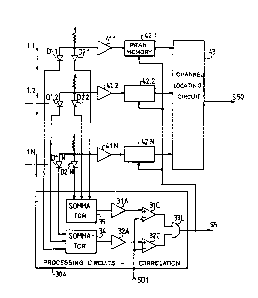
15According to the second embodiment shown in figure 6,
the system has N optical channels and 2N detection
channels. Each detection channel has the amplifiers 31A and
32A downline of the detectors. These amplifiers are
followed by a peak memory circuit 42.1 to 42.2N. An
electronic assembly 30B comprises a summation circuit 36,
- powered by the 2N outputs of the detectors and
series-connected with an amplifier 37A, followed by a
threshold comparator 38C. The signal S10 given by this
assembly is applied firstly, to the peak memory circuit 42
and, secondly, to a unit 30C for processing by correlation
12
:~
. ~ .
-
1 ~27842
according to the invention. In this processing unit, the
signals S3.J and S4.J of each pair of detectors are
correlated and give true detection when the signal is the
useful signal present simultaneously at each detecting
channel of the order J optical channel considered.
The processing circuit 30C may consist of a battery of
correlators after the shaping of the signaL or, preferably,
as indicated, with a digital/analog converter circuit 50
followed by a processor 51 which performs the false alarm
processing operations by correlation in comparing the
signals S3.J and S4.J with each other for the N channels.
It must be noted that the processor circuit can perform the
locating processing operation at the same time since it has
the information on the amplitude of the signal after the
digital conversion at 50, and since it also has the
information on the origin of signal, namely, on the channel
from which it comes. Consequently, in ~his embodimentl the
output S5 validates the useful signal and may also comprise
the information on the channel, namely the direction of the
elementary eJ in which the detected signal is received.
According to a third embodiment of figure 7, an output
signal S5 is also obtained here and comprises both the
selection of the useful signal with the elimination of the
spurious pulses and the information on the optical channel
from which this signal comes. According to this embodiment,
13
~ ; , .;
-,. . ................. .. . .. .
;~ . : , - ,; . ~ . .
.:: ., . : .
.~ : :
- =
1 327842
the number of amplifiers 39.1 to 39.N and the number of
peak memory circuits 42~1 to 42.N is equal to N and is
thereore divided by 2, thus increasing the compactness of
the equipment. The N detecting channels originate, as
shown, from a pair of detecting elements, but one of them
relates to an optical channel l.J and the other relates to
the following optical channel l.tJ + 1). This is got with
the summation circuits 45.1 and 45.N. The detected outputs
S3~.1 to S34.N are applied, as previously, to a circuit 30C
for processing by correlation.
The embodiment of figure 6, compared with that of
figure 5, ha~ the advantage of not being critical for the
coupling between channels. On the contrary, it is more
complicated if the number of channels N is great. For the
last two embodiments according to figures 6 and 7, it may
be worthwhile to use 2 detectors integrated in the same
package, for example, a two-cell package, for each channel.
The last embodiment shown in figure 7 which is
simpler, is more compact and is the preferred version.
,: . , . : : ~ : .
.'' ~ : ' ' '
i, . . ' : '