Note: Descriptions are shown in the official language in which they were submitted.
~327a~6
- 1 - RCA 80382/B0382A
IMAGE STORAGE USING SEPARATELY SCANNED
WIDEBAND AND NARROWBAND VARIABLES
This is a division application of Canadian
Application Serial No. 549,078, filed October 9, 1987.
The invention relates to image storage in
television display systems as may, by way of example, be
used in computer apparatus.
A small computer may ~e used to decode
television display material that has been encoded in an
economical format (e.g., to permit the transmission of
image data via telephone lines or the recording of image
data on compact disc). This small computer may be
provided with general-purpose memory, portions oE which
are available for use as image memory to provide buEfering
between an irregular flow of received image data and the
regular flow of image data to the display. It is
desirable to provide an image memory configuration that is
well suited to being used interchangeably with other data
storage in general-purpose memory and does not require the
use of dedicated portions of the memory for image storage.
The encoding of television information for
transmission over media of such limited bandwidths as those
available from a telephone line or compact disc forces the
designer to resort to powerful video compression methods.
These methods rely upon transmitting as little new image
information per frame as possible and upon storing as much
old image information as possible; and transmission of new
image information cannot be done, at least not entirely, in
real time. ~n order to write a~display in real time, then,
it is essential to have frame buffer storage memory with the
capability of storing at least two frames of video
information. Such memory can be written to from a flow of
compressed image data received in non real time and read
from so as to supply the display apparatus with a regular
flow of image data in real time. The frame buffer stor~e
~ .
: '~; '" ;'
: ; ,!
1 3278~6
-2- RCA 80382/80382A
memory is bit-map-organized for convenience in constructing
updated images from previous image data in accordance with
instructions included in the compressed video data.
In present-day practical terms such a frame
buffer storage memory is a large amount of memory.
Sampling chrominance information more sparsely in space
than luminance information can substantially decrease the
amount of information to be stored. E.g., where
chrominance is sampled one quarter as densely as luminance
in the directions of line trace and of line advance, a
sixteen times reduction in the amount of chrominance
information to be encoded results. If chrominance is
described in terms of two orthogonal color-difference
signals each having the same number of bits resclution as
luminance, which is commonly the case, the amount of
chrominance information to be stored in the frame buffer
storage memory is reduced from twice the amount of
luminance inormation to be encoded to only one-eighth the
amount of luminance information to be encoded.
Image memories, the addressable storage locations
of which map corresponding picture elements or "pixels" on
a display screen and which store single bits descriptive of
whether those corresponding pixels are bright or dark, have
been described as being "bit-map-organized" for many years.
In recent years the term "bit-map-organized" has been
applied to certain image memories in which a pixel variable
related to brightness is not expressed in terms of a single
bit, but rather in terms of a plurality of bits. Such
brightness-related variables may be luminance variables or
may be color-difference variables used in connection with
describing cslor displays, for example. The term
"bit-map-organized" has been extended to refer to two
different memory configurations, each storing a plural-bit
value descriptive of a pixel variable.
A plural-bit-variable bit-map-organized image
memory of a fi~t g~ne~dl ~ype knowr, irl th~ PrL~ aL ~ ~an
be thought of as having employing a number of bit planes,
-1 327846
~3- RCA 80382/80382A
which number equals the total number of bits in the
plural-bit-variable(s) describing a single pixel. The most
significant bits of a first of the pixel variables are
stored in the first bit plane at storage locations having
5 respective addresses mapping respective pixel locations in
the display; the next most significant bits of the first
pixel variable are stored in the second bit plane at
storage locations having respective addresses mapping
respective pixel locations in the display in a manner
10 corresponding to the mapping of the storage locations in
the first bit plane; and so forth, proceeding to less
significant bits in the first pixel variable, then
proceeding through the bits of each other pixel variable
(if any) proceeding ~rom most significant to least
15 significant bit. Responsive to a single address this type
of memory furnishes s1multaneously the respective plural
bits of all the pixel variables descriptive of a particular t
pixel. Essentially, the spatial positions of individual
pixels in the display have a one-to-one correspondence with
20 respective image memory addresses, in a spatial mapping.
This spatial mapping is held together by the tracing of the
display screen and scanning of image memory addresses each
being done in accordance with a prescribed pattern of
correspondence between these activities. So long as the
25 pattern of correspondence between these activities is
adhered to, the rate at which and order in which these
activities are carried out do not affect the spatial
mapping between the image memory addresses and the spatial
positions of display pixels.
Variants of the first type of image memor~ exist
in which the bit planes are not co-addressed, but are
addressed with prescxibed offsets as componen~s of a larger
bit plane. Each pixel output is not taken in parallel from
memory, hut serially through polling of the bit planes.
Such image memory is at present too slow for use with
moving imayes.
,;
.:
~ ' , , ,
~' . . ' .
~ .
1 327~4~
-4- RCA 80382/80382A
A second general type of plural-bit-variable
bit-map-organized image memory known to the prior art ~oes
not require a o~e-to-one correspondence between image
memory address and the spatial positions of display pixels.
There is a list of the values of the plural-bit pixel
variables in a prescribed cyclic order, which cycles are
arranged in the sequence of the tracing of the spatial
positions of pixels in the display. The :List is converted
to a string of values of the pixel variab:Les, with the bits
in each value arranged in prescribed ordex accordina to
relative significance. Each string of values is divided
into words of given bit length, which words are stored
respectively in successively addressed locations in the
image memory. An image memory of this second general type
has t~ be read out to a formatter with pixel unwrapping
capability. The formatter reconstitutes the words into a
string of values which are then parsed back into successive
values of each pixel variable. The variables for each
pixel are temporally aligned by the formatter to be
available at the time the spatial position of that pixel is
reached in the scanning of the display screen.
When a pixel is described in terms of plural
variables--e.g., a luminance variable and two chrominance
variables--it has been a general practice to group these
variables in a prescribed order for each pixel and to use
each group as subvariable componer.ts of a respective value
of a complex pixel-descriptive variable. The values of
this complex variable are then stored in a
bit-map-organized image memory organized as either the
first or the second type of image memory described above.
This practice is reasonably satisfactory as long as the
pixel-descriptive variables used as subvariable components
of the complex variable are sampled at corresponding points
in display space and with the same sampling density.
However, it is desirable to be able to sample the pixel
variables at diff~Lin~ sam~ling densities in order to
conserve image memory and to permit faster image
, :~
: :
,.
i3278~6
-5- RCA 80382/80382A
processing. ~hen, this method of using complex
pixel-descriptive variables becomes unattractive.
J. A. Weisbecker and P. K. Baltzer in U.S. Patent
No. 4,206,457 issued 3 June 1980 and entitled "COLOR
DISPLAY USING AUXILIARY MEMORY FOR COLOR INFORMATION"
describe an image memory comprising a luminance-only
memory, the read addresses of which map display space
according to a densely sampled bit-map organization, and a
chrominance~only memory, the read addresses of which map
display space ac~ording to a sparsely sampled bit-map
organization. Separate memories, which they refer to as
"data memory" and as "small auxiliary memory", are
dedicated to the storage respectively of luminance-only
information and of chrominance-only information,
respectively. The read addresses for the auxiliary memory
are the more signiicant bits of the read addresses for the
data memory in a scheme for accessing the memories in
parallel during reading out from image memory. The
Weisbecker and Baltzer configuration of image memory is a
variant of the first general type of plural-bit-variable
bit-map-organized memory, it is pointed out.
The Weisbecker and Baltzer memory architecture
dedicates specific portions of a combined image memory to
luminance and dedicates other specific portions to
chrominance. Video image storage systems are known where
chrominance subsampled respective to luminance for storage
in digital memory is spatially interpolated to generate
re-sampled chrominance of the same sampling density as
luminance, with similar-sample-rate luminance and
chrominance signals being linearly combined to generate
component-primary-color signals (i.e., red, green and blue
signals). Not only can linear interpolation in the
direction of scan line extension be used. Bilinear
interpolation, wh~re there is linear interpolation both in
this direction and in the direction transverse to scan
lines, can also be u~ed, LuL ~Xdl~l~ie,
' ` ~ '~ ''~' '
-1 327846
-6- RCA 80382t80382A
Because o~ the desire to reduce storage
requirements ~or image memory, which can be accomplished
without immediately perceptible degradation of the
displayed image by sampling chrominance less densely than
luminance, particularly if the image is camera-originated,
there is a strong impetus for the designer to configure
image memory along the lines suggested by Weisbecker and
Baltzer. ~owever, in the Weisbecker and Baltzer
configuration of image memory, the number of
pixel descriptive bits associated with an image memory
address changes, depending on whether or not a spatial
position in the display does or does not have a chrominance
value as well as a luminance value associated with it.
This interferes with the shifting of bit-map-organized
image information in the image memory unless the memory is
allowed to have unused bits of storage in it. This,
however, undesirably negates to some degree the advantage
of sampling chrominance more sparsely in space than
luminance. The ability to shift image portions readily in
image memory is important in the reconstruction of dynamic
images in image memory responsive to compressed video data.
The inventors find it is also unattractive to use
complex pixel-descriptive variables in variants of the
second general type of plural-bit-variable
bit-map-organized memory that subsample chrominance as
compared to luminance. The complex pixel-descriptive
variables are intermixed with luminance-only pixel
descriptive variables in the image memory read out. This
presents complex data-parsing problems, especially when
shifting of image portions in memory takes place in the
decoding of compressed video data.
A type of dual-ported, dynamic random-access
memory that has recently become commercially available is
~he so called "video random-access memory" or "VRAM". This
dynamic memory, in addition to a random-access input/output
port through wlli~h ill~o1mation car. be wri~ei-. irl~o or ledd
out of the memory, has a serial-access port from which a
:,,, A
"
'`
.~
~ 327846
-7- RCA 80382/80382A
row of data can be read serially at video scan rates. The
row busses of a principal dynamic random-access memory
portion of a VRaM are arranged to transfer data in parallel
to a smaller auxiliary memory of the VRAM, during an
interval equal to the read interval from the random-access
port. A counter is provided in each VRAM for scanning the
addresses of the auxiliary memory during its readlng, so
the auxiliary memory can function as a shift register.
After parallel loading of the auxiliary memory, its
contents are read out serially through the VRAM serial
output port, with the counter counting at a relatively high
clock rate. This clock rate can be the rate at which the
luminance-only picture elements are delivered to the
display monitor of the computer apparatus, for example.
This speed of reading is possible because the
capacitance-to-substrate of the auxiliary memory busses is
relatively low owing to the smaller size of this auxiliary
memory. It is attractive, then, the present inventors
point out, to use VRAM for the general-purpose memory
capable of storing television images, with both the
luminance-only information and the chrominance-only
information being read out through the serial output port
on a time-division-multiplexed basis, although conventional
random-access memory can also be used.
In some types of VRAM data can also be sexially
read into the auxiliary memory via the serial-access port,
to be transferred in parallel into the principal dynamic
random-access portion of the VRAM. This allows faster
writing of the VRAM than is possible by writing information
via its random-access port.
Television transmission systems are known where,
in order to avoid chrominance information in an analog
signal cross-talking with luminance information in an
analog signal, lines of chrominance information are time-
compressed and are time-interleaved between lines of
luminance information. Tll~ ti~ coln~-css~ul-n arld tirhe
displacement of chrominance is carried out in the digital
.;
: :
: ,:
,
. .
1 327846
'8- RCA 80382/80382A
domain, then transformed to the analog domain by
digital-to-analog conversion. These systems are known as
"Multiplex Analog Component" transmission systems or "MAC"
transmission systems. Luminance/chrominance crosstalk is
not a problem in digital television transmission systems
such as those considered herein, where luminance samples
and chrominance samples are kept separate from each other.
The present inventors discerned that time
interleaving of lines of digitized chrominance information
with lines of digitized luminance information is usefully
applied to the reading of VRAM through its serial access
port, in that it permits the use of separate bit-map
organizations for luminance and chrominance variables in
VRAM. The use of separate bit-map organizations for
luminance and chrominance variables the present inventors
perceived would avoid the problems encountered in the use
of complex pixel-descriptive variables in a unified bit-map
organization when chrominance is sampled less densely in
display space than luminance is. The use of separate
bit-map organizations can be accommodated by using a
ra~e-buffering memory for at least the chrominance samples r
the present inventors realized.
In television receivers processing conventional
alternate-field line-interlaced television signals to
provide progressive scan at doubled horizontal scan rates,
a rate-buffering memory is used to receive and delay
expanded information, both for luminance and for
chrominance. This rate-buffering memory is used for a
further purpose, as well, to provide the sample bed
information to support spatial interpolation in the
direction transverse to line scan. For example,
W. N. Hartmeier describes such apparatus in U.S. Patent
No. 4,580,163 issued l Apxil 1986 and entitled "PROGRESSIVE
SCAN VIDEO PROCESSOR HAVING PARALLEL ORGANIZED MEMORIES AND
A SINGLE AVERAGING CIRCUIT". Three line storage memories
~re o~er~t~d ~ a ey~lie wriLe-one, re~d--wo ~aSiS Lo
": '
~', ,: ,
1 327846
-9- RCA 80382/80382A
provide spatial interpolation in the direction transverse
to the line scan. The present inventors developed simpler
structures using only two line storage memories for
providing rate~buffering and spatial interpolation
following VRAM read-out in television display systems of
the type with which they are concerned.
SI~MMARY OF THE INVENTION
Time-division-multiplexing of lines of wideband
video (e.g., luminance) information and lines of narrowband
video information (e.g., chrominance) in the reading out of
VRAM used as image memory is done in image memory systems
constructed in accordance with the invention. ~his allows
separate bit-map organiæations in image memory of wideband
video information and of narrowband video information; an~
it facilitates the wideband video information and
narrowband video information both passing through the VRAM
serial output port, while avoiding complicated parsing of
VRAM serial output data into wideband video and narrowband
video portions.
Wideband video information is read out from VRAM
image memory in real time at the video scan rate, during
the display line trace intervals, without need for rate
buffering in preferred embodiments of the invention.
Alternatively, wideband video information may be
i 25 rate-buffered between the VRAM image memory and the
display. Narrowband video information is read out in
compressed and displaced time, preferably during the
display line retrace intervals. Rate bufferiny and spatial
interpolation are then used to place the narrowband video
informatiQn into proper temporal relationship vis-a-vis the
wideband video information with which it is combined for
generating drive signals for the display apparatus.
A further aspect of the invention is simplified
structure for performing the rate-buffering and spatial
interpolation of the na,rowband video in'ormation. In the
present invention the VRAM supplies to rate-buffering
: ,: . -
.,:, - , -~: ,
-: . .. : ~: , :
1 ~27846
-10- RCA 80382/80382A
memory narrowband video data that is compressed in time,
rather than expanded in time, as compared to the response
to that video data as it appears on screen. This allows
spatial interpolation to be supported with a rate-buffering
memory that is more economical of parts than prior-art
spatial interpolators. Two line-storage memories suffice
to provide spatial interpolation in the direction
transverse to line scan when a 2X2 bed of samples is used
in bilinear interpolation, for example. Alternate ones of
successive scan lines of narrowband video data in a field
scan are successively written into the first line storage
memory during display line retrace intervals or during
selected ones of those intervals; and the other remaining
scan lines of narrowband video data in that field scan are
successively written into the second line storage memory.
These two line storage memories are read out during di.splay
line trace intervals. The read outs are permuted, weighted
and linearly combined to complete spatial interpolation in
at least the direction of line scan.
A still further aspect of the invention is the
configuring of the VRAM using separate bit-map
organizations of wideband video information and of
narrowband video in~ormation r to implement the
time-division-multiplexing of lines of wideband video
information and narrowband video information.
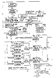
FIGURE 1 is a schematic diagram of a television
display system which includes chroma resampling apparatus
and embodies the invention.
FIGURE 2 is a schematic diagram of a basic
interpolator block, used as a building block in
interpolators that may be used in implementing the FIGURE 1
television display system.
FIGURES 3 and 4 are schematic diagrams of two
interpolators, each constructed using one or more FIGURE 2
basic inter~olat~r blOcka~ and ~ach applica~le for use ~n
the FIGURE 1 television display system.
.
.~ :., . :
. .;
:
~ 3278~6
-;1- RCA 80382/80382A
FIGURE 5 is a schematic diagram of video
random-access memory architecture used in the FIGURE l
television disp~ay system.
FIGURE 6 is a schematic diagram of circuitry for
generating the serial output port address,ing for the FIGURE
5 memory architecture.
FIGURE 7 is a schematic diagram of alternative
chroma resampling apparatus to replace that shown in FIGURE
1 .
FIGURE 8 is a schematic diagram of a modification
that can be made to either the FIG~RE 1 or the FIGURE 7
television display system, to provide for rate-buffering of
luminance information read out of V~AM in further
embodiments of the invention.
FIGURES 9-16 are diagrams of how VRAM rows can be
packed with image data in accordance with the invention.
FIGURES 17-20 are schematic diagrams of circuits
for controlling the transfer of chrominance data from VR~
to the chrominance resampling apparatus in different
20 particular embodiments of the FIGURE 1 television display
system.
FIGURE 1 shows a television display system which
converts television imagery, stored in compressed form on a
compact disc, to a real-time display. A compact disc
25 player 2 supplies the television imagery in coded form to a
drawing processor 3. (Another data source, such as a
Winchester disc, may be used instead o compact disc player
2.) The imagery coding is designed to describe di~ferences
of a current image from recent images already reconstructed
~ 30 and stored in the image memory portions of a video
J random-access memory (or VRAM) 4, to lessen redundancy in
I the imagery coding. (VRAM 4, as will be explained in
,¦ detail further on, is in actuality a banked array of
~ component monolithic VRAM5. ) Drawing processor 3 has a bus
l 35 connecti~l 5 to the rea~/writ~ ra.,dom-access pOï t of V~ A
i and to VRAM 4 control circuitry that allows drawing
".
~`
, .......... .
.,
,. . , . ,: ~:
,.:: ,
. . .
1 3278~6
-12- RCA 80382/80382A
processor 3 to read out to its~lf any of the images stored
in VRAM 4 and that allows drawing processor 3 to write a
current or upda~ed image into the image memory portion of
VRAM 4. VRAM 4, in addition to its random-access
input/output port, has a serial output port 6 from which a
row of data can be read serially at video rates.
The nature of the stored images in VRAM 4 is of
particular concern to the invention. The image me~ory
portions of VRAM 4 are separately bit-map-organized with
respect to luminance samples and with respect to
chrominance samples. In a bit-map organization of image
memory, the storage locations in memory conformally map
descriptions of the picture elements, or "pixels", of the
display subsequently constructed from the read-out of that
image memory. One can arrange to bit-map pixels so
luminance and chrominance samples are combined at each
storage location in image memory. However, sometimes
luminance samples are more densely packed in space than
chrominance samples are. Furthermore, sometimes the ratio
of the sampling densities in space of luminance samples and
of chrominance samples is subject to variation. To include
chrominance samples together with only selected luminance
samples in a single bit-map organization would tend to
result in underutilization of memory at such times. This
is because, practically speaking, each storage location
would have to have the capability of storing chrominance
information whether or not it was actually available for
that point in the bit-mapO
The inventors avoid this problem by using
densely-sampled-in-space bit-map organization for luminance
samples in o~e portion of image memory and using a separate
sparsely-sampled-in-space bit-map organization for
chrominance samples in another portion of image memory. It
is convenient to make the sparser spatial sampling a
subsampling of the denser spatial sampling. Where the
ra~io of ~he spatial sampl ng densl.ies varies, the
apportionment of image memory between luminance samples and
chrominance samples changes.
1 327846
:13- RCA 80382/80382A
During line trace intervals in the display, lines
of luminance samples from the more densely sampled
bit-map-organized portions of image memory that have been
loaded in paraliel into the VRAM 4 auxiliary memory are
read out serially through the serial output port 6 of VRAM
4 to a formatter 7. Formatter 7 performs
"pixel-unwrapping" functions to furnish pixel data
concerning either luminance or chrominance. The way
formatter 7 operates will be described in more detail
further on. During line trace intervals formatter 7
re-times the luminance samples (supposing them to have
been "linearly packed" in VRAM 4, as will be described in
greater detail further on) so they are supplied at pixel
scan rate to a digital-to-analog converter 8. Converter 8
supplies to video matrixing circuitry 9 a continuous analog
Yl response to these luminance samples.
During selected line retrace intervals in the
display, lines of samples of first and second chrominance
variables Cl and C2 from the less densely sampled
bit-map-organized portions of image memory are selected for
read out from VRAM 4 via serial access output port 6 to
formatter 7. A way to do this is to read out a line of C
samples followed by a line of C2 samples during each
selected line retrace interval. This permits separate
bit-map organizations for Cl and C2, which simplifies the
drawing processor 3 required for converting coded imaqery
from compact disc player 3 to bit-map organization image
data in VRAM 4. Simplification arises because calculations
involving C1 and C2 can be performed separately and
serially, such calculations being made with simpler
interfacing between drawing processor 3 and VRAM 4. The
time-division-multiplexing of Cl and C2 output signals from
formatter 7 to converter 8 and to a chroma resampling
apparatus 10 during display processing is also simplified,
since the multiplexing rate during line retrace intervals
is lowO
i
., : ,
-
1 327~6
RCA 80382/80382A
Formatter 7 performs further pixel-unwrapping
functions, in separating successive Cl and C2 samples in
the supplying of separate bit streams of Cl samples and of
C2 samples to the chrominance resampling apparatus 10. If
VRAM image memory is read out in the preferred way, a bit
stream of Cl samples is supplied to chrominance resampling
apparatus 10, followed by a stream of C2 samples. The
chrominance re-sampling apparatus 10 re-samples the
digitized Cl and C2 variables to the same sampling density
as the digitized luminance, Y. The Cl samples are supplied
to a digital-to-analog converter 11, which supplies its
analog Cl response to video matrixing circuitry 9. The C2
samples are supplied to a digital-to-analog converter 12,
which supplies its analog C2 response to video matrixing
circuitry 9. The chrominance resampling apparatus provides
time delay that brings the Cl and C2 samples supplied to
digital-to-analog converters 11 and 12 into proper
alignment-in-time with the Y samples supplied to
digital-to-analog converter 8. This allows the Y and Cl
and C2 signals to be matrixed together in video matrixing
' circuitry 9 to generate red (R) and green (G) and blue (B)
drive signals. These R, G and B drive signals are
amplified by video amplifiers 13, 14 and 15 respectively.
The amplified drive signals are then applied to kinescope
16 to generate the color display.
Still referring to FIGURE 1, a display
synchronizing generator 18 generates HORIZONTAL
SYNCHRONIZATION and VERTICAL SYNC~RONIZATION pulses for
application to the deflection circuitry l9 of kinescope 16.
Display synchronizing generator 18 also supplies signals to
VRAM read~out control circuitry 17 to inform it concerning
' display timing. For example, VRAM read-out control
circuitry 17 includes a line counter for counting
HORIZONTAL SYNC~RONIZATION pulses supplied from display
, 35 synchronizing generator 18. This line counter is reset to
zero by a BETWEEN FRA~iE ~ui~ u~ylieu '~y ~is~ldy
synchronizing generator 18 after the conclusion of each
frame of display and before the start of the next. Display
.~
,,
. ~ , ~ . . .
: : ~
~2 7 8 4 6 RCA 80382/80382A
sync generator 18 also supplies pulses at a multiple of the
pixel scan rate to control circuitry 17. Circuitry 17
scales from the~e pulses to generate an appropriate SERIAL
OUTPUT CLOCK signal for application to VRAM 4 and to
formatter 7.
The formatter 7 allows data to be taken out "full
width" from the serial output port 6 of VRAM 4, so the
clock rate at which data is clocked from port 6 can be kept
to a minimum. For example, if port 6 is thirty-two bits
wide, then during the line trace interval, each 32-bit word
read out through port 6 can be apportioned into four
successive eight-bit luminance samples by formatter 7,
permitting the VRAM output to be scanned at one-quarter of
the pixel scan rate. Formatter 7 does this formattirlg
responsive to instructions from control circuitry 17.
Control circuitry 17 also selects the rows in VRAM 4 to be
transferred in parallel to the VRAM 4 shift register that
thereafter shifts its contents out through serial-access
output port 60 VRAM read-out control circuitry 17 also
applies the correct SERIAL OUTPUT CLOCK signal to this
shift register for this shifting procedure.
Continuing the example, suppose the chrominance
samples Cl and C2 are all eight-bit samples and are
spatially subsampled every fourth luminance sample in ~very
fourth line of luminance samples. During a selected line
retrace interval, conventionally one fifth as long in
duration as a line trace interval, the number of samples in
Cl and the number of samples in C2 each is one-quarter the
number of samples of the luminance signal Y during a line
trace. Each thirty-two-bit word read out through port 6
during a line retrace interval is apportioned into four
successive eight-bit C1 samples or four successive
eight-bit C2 samples, for application to chrominance
resampling apparatus 10. Since the number of samples of C
per one of its scan lines and the number of samples of C~
per one of its scall lines are each one-quar~e}- the nu~er
of samples of luminance per one o~ its scan lines, the
total number of samples of chrominance per one of its scan
.: , ,
~: , , ;.. -, . . . .
~ 327846
-16- RCA 80382/80382A
lines is one half the number of luminance samples per one
of its scan lines. Since the total number of samples of
chrominance per one of its scan lines is to be transferred
from VRAM 4 serlal output port 6 in a line retrace interval
one fifth the duration of the line trace interval in which
luminance samples are displayed, VRAM read out control
circuitry 17 has to increase the SERIAL OUTPUT CLOCK rate
during line retrace by a factor of at least 2~ times.
If clock rates are scaled only by powers of two
from a high rate master clock signal, the serial clock rate
used to read from VRAM 4 during line retrace interval will
be four times the pixel scan rate for luminance. This
reduces the time needed for accessing VRAM 4 for obtaining
chrominance samples to less than a complete line retrace
interval, freeing output port 6 for downloading other data
during the remalning portion of the line retrace interval.
The chrominance resampling apparatus 10 includes
line-storage random-access memories 101, 102, 103 and 104.
,A selected pair of these line-storage memories are written
responsive to C1 samples and C2 samples supplied to them
respectively from formatter 7 during selected line retrace
intervals. Line~storage memories 101 and 102 are written
alternately by successively selected lines of Cl samples,
and memories 101 and 102 are read out during line trace
intervals to supply adjacent lines of Cl samples in
parallel to a two-dimensional spatial interpolator 105.
Line-storage memories 103 and 104 are written alternately
by successively selected lines of C2 samples. Memories 103
and 104 are read out during line trace intervals to supply
adjacent llnes of C2 samples in parallel to a
two-dimensional spatial interpolator 106. Interpolators
105 and 106 supply resampled signals C1 and C2 to the
digital-to-analog converters 11 and 12, respectively. C
and C2 are each resampled to the same spatial sampling
density as Y.
FIGURE 2 shows a novel ~asic inLerpGla~ O! block
20 that can be used as a basis for the construction of each
of the interpolators 105 and 106, to provide for each of
1 327846
-17 RCA 80382/80382A
them being bilinear interpolators. The output pixel scan
rate from the block 20 is double khe input pixel scan rate
to its input terminals IN and IN'. Respective streams of
pixel samples from adjacent scan lines in subsampled image
space are repetitively supplied at output scan line rate to
terminals IN and IN' of interpolator block 20. Each scan
line in subsampled image space is repeated either 2(n+l)
times, or one less time, where 2n:1 spatial interpolation
is performed in the direction transverse to scan lines, n
being a positive integer at least unity. Repeating the
scan lines 2(n 1) times simplifies the clocking of the line
store RAMs 101-104. In either case, the line store RAMs
101-104 can be loaded during two successive line retrace
intervals, rather than just one.
A multiplexer 21 responds to a CONTROL 1 signal
to select the one of the streams of pixels applied to
terminal IN and IN' for spatial interpolation that is
earlier-in~time in the direction of line scanning. As a
first step in this interpolation the selected ~tream of
pixels is applied to a one-pixel-delay circuit 22. The
pixels from the selected stream are summed in an adder 23
with the pixels from the selected stream s delayed one
pixel by circuit 22, and the resultant sum is divided by
two in a bit-place shifter 24 to supply the average of two
successive pixels in the stream selected by multiplexer 21.
A multiplexer 25 alternately selects to the terminal OUT of
interpolator block 20 the delayed pixel output of circuit
22 and that average of two successive pixels. This
selection by multiplexer 25 is made at the pixel output
rate that is twice the pixel input rate.
Terminal OUT' of interpolator block 20 sllpplies
another stream of pixels at this pixel output rate,
representative of an interpolated scan line preceding the
scan line supplied through terminal OUT. This interpolated
scan line i5 generated as follows. The streams of pixels
suppli~d to ~erminals IN and IN' of interpolator blGck 20
are summed in an adder 26 and applied to a one-pixel-delay
circuit 27. The output of circuit 27 is divided by two by
, . .
1 3 2 7 8 4 6
-18- RCA 80382/80382A
a one-bit-place shifter 28 to supply pixels for the
interpolated scan line which are intexpolated only in the
direction trans~erse to the scan line direction. Pixels
for the interpolated scan line which are also interpolated
in the direction of the scan line are generated by (l)
summing in an adder 29, the adder 26 output and the adder
26 output as delayed one pixel in circuit 27 and ~2)
dividing the resultant 5um from adder 29 by four in a
two-bit-place shifter 30. A multiplexer 31 alternately
selects to terminal OUT' of interpolator block 20 the
pixels for the interpolated line scan that are not
interpolated in the direction of line scan and those pixels
that are. This selection by multiplexer 31 is made at the
pixel output rate, which is twice the pixel input rate.
Interpolator block 20 resamples its input data as
supplied to terminals IN and IN' to provide at its
terminals OUT and OUT' samples at 4:1 higher scan rate.
However, these samples are not in regular scan line order.
FIGURE 3 shows how interpolators 105 and 106 of
20 FIGURE 1 can be constructed using ~wo basic interpolator
blocks 20-1 and 20-2 together with multiplexers 32 and 33 !
when 2:~ spatial interpolation is desired both in the
airection of scan line extension and in the direction
transverse to the scan lines. Multiplexers 32 and 33
operate to place the higher scan rate C1 and C2 samples in
regular scan line order. Line storage RAMs 101, 102, 103
and 104 are each read four lor three) times before being
xe-written. When interpolator~ 105 and 106 are constructed
per FIGURE 3, RAMs 101 and 103 are written simultaneously,
and R~Ms 102 and 104 are written simultaneously. There is
a two-scan-line offset between the writing of R~Ms 101 and
103 and the writing of RAMs 102 and 104, when the
interpolators 105 and 106 are constructed per FIGURE 3.
Interpolation control circuitry 34 supplies
CONTROL 1 signal at the input line advance rate to ~oth the
basic interpolator ~lo~k~ 20-1 all~ 20-2. Cil-~ui~ry 3~ also
supplies them both with the CONTRO~ 2 signal at twice the
input scan rate (which in the FIGURE 3 interpolators equals
,
- , . .. . .
~ 327846
-19- RCA 80382/80382A
the output pixel scan rate). Circuitry 34 further supplies
a CONTROL 3 signal switching at input line advance rate to
each of the mul~iplexers 32 and 33. Multiplexers 32 and 33
provide input data for digital-to-analog converters 11 and
12 by selecting the two interpolated signals from the
terminals OUTI of blocks 20-1 and 20-2 respectively during
one set of alternate output lines. During the intervening
set of alternate output lines, multiplexers 32 and 33
provide input data for converters 11 and 12 by selecting
the two interpolated scan lines from the t~rminals OUT of
blocks 20-1 and 20-2 respectively. Multiplexer 32 arranges
the output scan lines of Cl in correct sequential order,
; compensating against the reversals of scanning line order
in line-storage ~AMs 101 and 102 accepted in order to
reduce the fregAuency of their re-writing. In like manner
multiplexer 33 arranges the output scan lines of C2 in
correct sequential order, compensating against the
~, reversals of scanning line order in line-storage RAMs 103
`i and 104. Cascade connections of pluralities n in number of
1 20 basic interpolator blocks replacing the single basic
interpolator blocks 20-1 and 20-2 can be used to implement
2n:1 spatial interpolation both in the direction of scan
line extension and in the direction transverse to scan
lines.
, 25 FIGURE 4 shows how interpolators 105 and 106 can
be constructed to provide 4:1 spatial interpolation in each
of these directions. Basic interpolator block 20-1 is
followed in cascade connection by another basic
interpolator block 20-3 and multiplexer 32 in this
embodiment of interpolator 105. Basic interpolator block
20-2 i5 followed in cascade connection by another basic
I interpolator block 20-4 and multiplexer 33 in this
embodiment of interpolator 106. Line storage RA~s 101,
j 102, 103 and 104 are each xead eight (or seven) times
~l 35 before being re-written when interpolators 105 and 106 are
~ constructed pe~ FIGURE 4. RAIrAs 10; ar,d 103 are Wl-i~te.
i simultaneously, and RAMs 102 and 104 are written
~imultaneously. There is a four-scan-line oEfset between
'. ' '
. ~ :
1 327846
-20- RCA 80382/80382A
the writing of RAMs 101 and 103 and the writing of RAMs 102
and 104, when the interpolators 105 and 106 are constructed
per FIGURE 4.
Interpolation control circuitry 35 supplies the
CONTROL 1 signal to both the blocks 20-1 and 20-2 at one
half their output line advance rate. Interpolation control
circuitry 35 also supplies the CONTROL 2 signal at twice
the pixel scan rate from line-storage RAMs 101-104 to both
of the blocks 20-1 and 20-2. In the FIGURE 4 interpolators
this rate equals one-half the output pixel scan rate.
Interpolation control circuitry 35 also supplies the
CONTROL 3' signal switching at the input line advance rate
to multiplexers 32 and 33~ As in the FIGURE 3
interpolation circuitry, multiplexers 32 and 33 compensate
for line scanning order reversals in line-storage RAMs
101-104.
Basic interpolator blocks 20-1 and 20-2 supply,
to basic interpolator blocks 20-3 and 20-4 in cascade after
them, twice as many input scan lines as they received from
the line storage RAMs 101-104~ Accordingly, interpolation
control circuitry 35 supplies a CONTROL 1' signal to the
CON~OL 1 signal connections of basic interpolator blocks
20-3 and 20-4 at one half their output line advance rate --
that is, at the output line ad~ance rate of basic
interpolator blocks 20-1 and 20-2.
Basic interpolator blocks 20-3 and 20-4 receive
pixels from basic interpolator blocks 20-1 and 20-2 at
twice the pixel scan rate from line-storage RA~s 101-104.
Interpolation control circuitry 35 supplies a CONTROL 2'
signal to the CONTROL 1 signal connections of basic
interpolator blocks 20-3 and 20-4 at the twice their pixel
input rate, which is four times the pixel output rate from
line-storage RAMs 101~104.
FIGURE 5 shows more particularly the cons~ruction
of one bank of VRAM 4, a thirty-two-bit-wide data bus 6
connecting VRA~i 4 ~erial output pGrt to furma,ter 7, and
formatter 7 which performs the pixel-unwrapping function.
VRAM 4 comprises at least one bank 40 of eight component
:
-1 327846
-21- RCA 80382/80382A
VRAMs. FIGURE 5 is ofered as an aid to understanding more
completely how the luminance information and chrominance
data can be sto~ed in separate bit-map organizations.
In preferred embodiments of the invention, the
bit-maps are stored in VRAM 4 as if the following mapping
procedure were followed. Each of the several bit-pixel
data is converted from parallel-bit to serial-bit format
according to a prescribed ordering rule. The successive
pixel data in each scan line are then strung together
seriatim. The resulting strings of bits descriptive of a
display scan line are then strung together in the order of
display scan line advance, so the description of a complete
image field is afforded b~ the resulting still longer
string of bits. This string of bits is then mapped into
successive rows of VRAM 4 in a procedure called "linear
packing". Linear packing permits the density of storage in
VRAM 4 to be as high as possible despite the bit-length of
the pixel codes being chosen from a plurality of code
lengths submultiple to the number of bits in a row of a
VRAM 4 bank, such as bank 40. A commercially available
component 64K X 4 VRAM contains four square dynamic memory
arrays 28 bits on a side, it also contains static memory
operable to provide four parallel-in/serial-out registers
as buffer memory to a four-bit wide serial output port. A
bank of eight such component VRAMs provides 256 rows of 256
four-byte digital words, and these dimensions will be
assumed by way of example for VRAM 4 throughout the
remainder of this specification.
The loading of the static memories in the
component VRAMs, which serve as bufer memories to the
serial output port of VRAM 4, is controlled by a SERIAL
READ-OUT ADDRESS CODE called SRAC for short. SRAC is a
three part code consisting of a first group of adja~ent bit
places containing a BANK ADDRESS, a second group of
adjacent bit places containing a ROW ADDRESS and a third
group of adjacerlt bit plac~s containing COLUMN ADDRESSES.
The ROW ADDRESS and COLUMN ADDRESS portions of SRAC are
descriptive of storage location placement in VRAM 4 and are
,,
, ~
1 327846
-22- RCA 80382/80382A
not directly related to the dimensions of the display
raster, the bit~map organization for luminance pixel codes
or the bit-map organization for chrominance pixel codes.
SRAC will be assumed to code BANK ADDRESS in its most
significant places, which is preferable to do from the
viewpoint of allowin~ easy add-on of more banks o
component VRAMs. SRAC will be assumed to code COLUMN
ADDRESS in the least significant group of eight bit places
and to code ROW ADDRESS in the next least significant group
of eight bit places. Each of the 2 values of BANK ADDRESS
is assigned solely to a respective bank of VRAM 4, and a
bank address decoder 37 for that bank 40 o VRAM 4 to which
the current value of those m bits is assigned responds to
that value to condition bank 40 of VRAM 4 for reading out
to the thirty-two bit wide data bus 6. This arrangement
makes possible the multiplexed connection of the banks 40,
etc. of VRAM 4 to bus 6.
The ROW ADDRESS portion of SRAC governs the
choice of row to he loaded for the serial-access output
port of at least the selected bank 40 of VRAM 4. Bank 40
~like the other banks of VRAM 4) comprises a respective
octet of component VRAMs 41, 42, 43~ 44, 45, 46, 47, 48
each having a four-bit-wide serial-access port. The number
of bits in a row of VRAM 4 serial output is 256 columns
times 32 bits per column, for a total of 213 bits. It is
convenient to describe the lumi~ance or chrominance
component signal of a display line in a number of bits
related to the number of bits per row of V~AM 4 in
integral-power-of-two ratio. A display line of
high-xesolution luminance component signal, for example,
might comprise 1024 eight-bit pixels so it is in 1:1 ratio
with a row in VRAM 4, in terms of numbers of bits. A
display line of intermediate-resolution luminance component
signal might comprise 512 eight-bit pixels and is thus in a
1:2 ratio with a row in VRAM 4, in terms of numbers of
bits. A di~iay li-~le uf 1~WeL-reSO1UtiGn 1-~m1nanCe
component signal might comprise 256 four-bit pixels so it
is in a 1:8 xatio with a row of VRAM 4, in terms of numbers
.:: , : , :
1 327846
-23- RCA 80382/80382A
of bits. Four display lines of a chrominance component
spatially subsampled 4:1 in both display~line-scan and
display-line-advance directions relative to these luminance
component signals would respectively be in 1~16, 1:32 and
1:128 ratios with a row of VRAM 4, in terms of numbers of
bits.
The COLUMN ADDRESS portion of SRAC specifies an
offset in the counter-generated addresses for the static
memories in component VRAMs 41-48 etc, during their
reading. The static memories in each component VRAM are
written in parallel from the associated dynamic memory in
that component VRAM with zero-valued offset. The serial
reading of the static memories through the serial output
ports of the component VRAMs in the selected bank 40 oE
VRAM 4 begins at the column location specified by the
COLUMN ADDRESS portion of SRAC. Where a plurality of
display lines of information are stored in a VRAM 4 row,
the COLUMN ADDRESS portion of SRAC permits the serial
output from VRAM 4 to commence at the beginning of any one
of the display lines of information.
Except when the number of bits in a display line
equals or exceeds the number of bits per row in V~AM 4/ the
row of VRAM 4 transferred to the static memories in the
component VRAMs 41-48 of the selected bank 40 generally
will not be fully read out before those static memories are
re-written. The underlying reason for this is that
luminance pixel codes are read from VRAM 4 during line
trace intervals through the same serial output port that
chrominance pixel codes are read from VRAM 4 during line
retrace intervals. This time-division-multiplexing between
two bit-map organizations requires that the static memories
be rewritten each time data from a different one of the two
bit-map organizations is to be read out.
Any particular bank of VRAM 4 can be selected
responsive to the BANK ADDRESS portion of SRAC, which has
m bits, wh~re 2m is the number of bar.ks of component VR~1s
in VRAM 4. Each bank of VR~M 4 has a respective bank
select decoder for decoding the BANK ADDRESS portion of
24 1 327846 RCA go3g2/80382A
SRAC, analogous to bank select decoder 37 for bank 40 of
VRAM 4. All component VRAMs in VRAM 4 have respective
TR/OE pins (not shown). A11 these TR/OE pins receive in
parallel a LOW logic condition as a TRANSFER signal at
S times of transfer of a row of data in any one of VRAM 4
banks to the static memory therein from which serial output
port is supplied data. The TR/OE pins for a selected bank
also receive a LOW logic condition as an OUTPUT ENABLE
signal when the random-access output/input port is accessed
in an aspect of operation not connected with the present
invention. The TRANSFER signal is executed as a command
only when a ROW ADDRESS STROBE signal is applied to a RAS
pin of each component VRAM involved. ~ank address decoder
37 applies a high-to-low transition only to the RAS pins of
the selected bank 40 of component VR~Ms 41-48 when a row of
data is to be transferred into the auxiliarv-static-memory
portions of component VRAMs 41-48.
A row/column address multiplexer 38 applies ROW
ADDRESS to the eight ADDRESS pins of the component VRAMs
41-48 to indicate which row of data is being transferred
for serial output. RAS is then allowed to go high, and
column address multiplexer 38 applies COLUMN ADDRESS to the
eight ADDRESS pins of component VRAMs 41-48. A COLUMN
ADDRESS STROBE is applied to the CAS pins of VRAMs 41-48;
this signal going low loads the internal address counters
of VRAMs 41-48 with appropriate offsets for serial read
out. CAS is then allowed to go high.
A pixel clock multiplexer 39 selects between the
LUMINANCE SERIAL OUTPUT CLOCK and CHROMINANCE SERIAL OUTPUT
CLOCK signals for application to the serial clock or SC
pins of the component VP~Ms. Bank address decoder 37
applies a LOW condition to the SOE pins of only the
selected bank 40 of component VRAMs as a SERIAL OUTPUT
ENABLE signal during the serial output from VR~M 4. This
conditions the serial output ports of componen~ VRAMs 41-48
to be multiplexed ~o ~e 32-bit-wid~ ~us 6. The ~UMINA`L~C~
SERIAL OUTPUT CLOCK and CHROMINANCE SERIAL OUTPUT CLOCR are
; both generated by a respective programmable division from a
MASTER CLOCK signal.
, . ., ~ . .
1 327846
-25- RCA 80382/80382A
Details of the ~onstruction of the formatter 7
for parsing the successive 32-bit words from the serial
output port bus 6 into pixels are shown in FIGURE 5. A
32-bit word register 50 holds thirty-two successive bits, a
number n of the most significant of these bits being the
code descriptive of luminance or chrominance. For
convenience n is constrai~ed to be an integral power of
two, sixteen or less. A programmable mask register 51
holds a group of n ONEs in the most significant of its
sixteen bit places and a group of (16 - n) ZEROs in the
least significant bit places. The contents of mask
register 51 and the sixteen most significant bits of the
word contained in register 50 have their corresponding bit
places ANDed in a bank 52 of AND gates to furnish selected
signal pixels of luminance or chrominance data. Where
these data are shorter than sixteen bits, the bit places of
lesser significance are filled by ZEROs. (In alternative
designs this data may be constrained to always be eight
bits or less, with mask register 51 being shortened to
eight-bit length and bank 52 including only eight AND
gates.)
When the first thirty-two bit word in a row of
VRAM 4 is supplied to formatter 7 via serial output port
bus 6, a multiplexer 53 admits that word to the 32-bit word
register 50. The n most significant bits of that word
defining a pixel datum are provided to the
digital-to-analog converter 8 shown in FIGURE 1 in the case
where a luminance bit-map in VRAM 4 is scanned, or are
provided to an appropriate one of the line store RAMs
30 101-104 of chroma resampling apparatus 10 in the case where
a chrominance bit-map in VRAM 4 is being scanned.
When the next (32~n)/n pixel data are being
provided to digital-to-analog converter 8 or to chroma
resampling apparatus 10, multiplexer 53 successively admits
the (32-n)/n successive output of a 32-bit multi-bit
shifter 54 to word registeL 5G. ~hifter 54 shifts n ~i LS
toward increased significance with each successive pixel as
timed by PIXEL CLOCK pulses.
, . . . .
:.
: :
,
-26-I 3 2 7 8 4 6 RCA 8o382/8o382A
As the modulo-n first pixel datum is to be
provided to digital-to-analog converter 8 or to chroma
resampling apparatus 10, multiplexer 53 admits a new 32-bit
word into register 50 instead of shifting the old word.
Multiplexer 53 can be controlled by decoding one output of
a modulo-n pixel counter, for example. This counter can
consist of the last n stages of a modulo-32 counter
counting at pixel clock rate, which counter together with a
binary shifter comprises multi-bit shifter 54.
One skilled in the art and provided with the
foregoing description of the interface between VRAM 4 and
formatter 7 will readily discern possible variants in the
VRAM 4 digital word organization and changes in the
formatter 7 architecture to accommodate these variants.
With each thirty-two-bit word read from VRAM 4, the pixel
order may be opposite to that described, for example, in
which case formatter 7 structure is altered as follows.
The programmable mask register 51 holds a group of n ONEs
in its least significant ~rather than most significant) bit
places. The group of (16-n) ZEROs are held in the most
significant bit places of mask register 51. The bank 52 of
sixteen A~D gates receives input from the sixteen least
significant Irather than most significant) bit places of
word register 50, as well as receiving input from mask
register 51 with its modified mask contents. The multi-bit
shifter 54 shifts n bits towards decreased significance
~rather than increased significance) with each successive
pixel as timed by PIXEL CLOCK pulses. Another variation
readily conceived of is that the column or word read
addresses in VRAM 4 may either increment or decrement as
the display is horizontally scanned.
FIGURE 6 shows details of construction of the
portion of VRAM read-out control 17 that generates SRAC in
FIGURE 1. SRAC is supplied to VRAM 4 from the output of a
multiplexer 59 that selects the correct SRAC for the
bit-map organization currel~tly ~ir;~- scanned. Thi~
facilitates keeping track of where each scanning is along
t 327846
-27- RCA 80382/80382A
the linearly packed data of its particular bit-map
organization. Two SRAC generators 60 and 70 are shown.
Generator 60 generates SRAC for successive lines of
luminance pixe~ data, Generator 70 generates SRAC for
successive lines of chrominance pixel data. To permit just
one SRAG generator 70 for both Cl and C2 descriptions of
chrominance rather than having to have two SRAC generators,
these descriptions are linearly packed in VRAM 4
interleaving C1 and C2 samples on a line by line basis.
SRAC generator 60 includes a SRAC latch register
61 for supplying a SRAC to one of the two inputs of
multiplexer 59. SRAC latch register 61 contents are
updated from the output of a multiplexer 62, controlled by
FIELD RETRACE BLANKING pulses. During ~ield retrace the
FIELD ~ETRACE BLANKING pulse causes multiplexer 62 to
select LUMA FIELD SCA~ START ADDRESS supplied from a start
address register 63, for updating register 61 contents.
LUMA FIELD SCAN START ADDRESS identifies the storage
location in VRAM 4 of the luminance pixel in the upper left
corner of the following field. These ~UMA FIELD SCAN START
ADD~ESSES are selected in prescribed order from a listing
in a portion of main computer memory reserved for storing
display instructions, and the listing of LVMA FIELD SCAN
START ADDRESSES is maintained by the drawing processor 3O
During field trace intervals in time, the absence
of FIELD ~ETRACE BLANKING pulse causes multiplexer 62 to
select the sum output of an adder 64 for updating SRAC
latch register 61 contents. Adder 64 has addenda supplied
to it from SRAC latch register 61 and from a programmable
display line pitch latch xegister 65. IMAGE LINE PITCH
stored in latch register 65 is the product of the number of
luminance samples per image line times the number of
luminance-descriptive bits per luminance sample times the
reciprocal of the number of bits per column address in VRAM
4 --i.e., the number of luminance-descriptive bits per
image line ~ivid d by thirty-t-wo. ~lements 61~65 are
operated as an accumulator augmenting SRAC by IMAGE LINE
PITCH during each line retrace interval. IMAGE LINE PITCH
:'
" ~ ' ' .
`` t 327846
-28- RCA 80382/80382A
is loaded into latch register 65 bY drawlng processor 3.
IMAGE LINE PITCH originates in compact disc player 2 or
other video source, and it can be convenient to carry it in
FIELD HEADER DATA preceding each field of bit-map-organized
luminance or chrominance pixel data in VRAM 4.
SRAC generator 70 includes a SRAC latch register
71 for supplying a SRAC to the other of the two inputs of
multiplexer 59. SRAC latch register 71 contents are
updated from the output of a multiplexer 72 controlled by
FIELD RETRACE BLANKING pulses. During a FIELD RETRACE
BLANKING pulse, multiplexer 72 selects a CHROMA FIELD SCAN
START ADDRESS supplied from a start address register 73,
for updating register 71 contents. CHROMA FIELD SCAM START
ADDRESS identifies the storage location in VRAM 4 of the
Cl pixel in the upper right corner of the following field.
These CHROMA FIELD SCAN START ADDRESSES are listed together
with LUMA FIELD SCA~ START ADDRESSES in the portion of main
computer memory reserved for storing display instructions,
and the listing of these CHRO~ FIELD SCAN START ADDRESSES
is maintained by the drawing processor 3.
During field trace intervals in time, the absence
of FIELD RETRACE BLANKING pulse causes multiplexer 72 to
select the sum output of an adder 7~ for updating SRAC
latch register 71 contents. Adder 74 has addenda supplied
to it from SRAC latch register 71 and from a programmable
display band pitch register 75. A chroma display band is
the number of display lines between the resampling of
chrominance values. C~ROMA DISPLAY BAND PITCH stored in
latch register 75 is the product of the number of
chrominance samples per chroma display band times the
number of chrominance-descriptive bits per chrominance
sample times the reciprocal of the number of bits per
column address in VRAM 4 -- i.e., the number of
chrominance-descriptive bits per chroma display band
divided by thirty-two. Elements 71-75 are operated as an
accumulator augmenting SRAC by C~ROMA DI~PLAY BA~D PITCn
1 327846
-29- RCA 80382/80382A
during selected line retrace intervals separated by
intervening chroma display band intervals. CHRQMA DISPLAY
BAND PITCH is lQaded into latch register 75 by drawing
processor 3 and originates similarly to IMAGE LINE PITCH.
Consider now the nature of the Cl and C~
chrominance signals used in the FIGURE 1 television display
system. Cl and C2 in this display system may be
color~difference signals that can be linearly combined with
the luminance signal Y using additive or subtractive
combining processes. The differences between Y and two of
the additive primary colors red (R), green (G) and blue ~B)
may comprise Cl and C2, for example. (R-Y) and ~B-Y) color
signals are often used. The color difference signals may
be formed by the differences between Y and other ~ixture
colors. I and Q signals similar to those used in the NTSC
television broadcast standard are examples of such color
difference signals.
C1 and C2 may also be color-difference signals
normalized respective to luminance signa1, [~R/Y)-1~ and
20 E (B/Y)-l~, or I/Y and Q/Y, by way of examples.
Normalization is removed from such a C1 and C2 signal by
multiplying by Y before linearly combining with Y.
FIGURE 7 shows an alternative chroma resampling
apparatus 100 that may replace chroma resampling apparatus
10 in the FIGURE 1 television display system. Chroma
resampling apparatus 100 permits the storage of chrominance
information in VRAM 4 in the form of read addresses for
chroma map memories 115 and 116 which store Cl and C2
values, respectively~ These read addresses can be
expressed in shorter-bit-length chrominance codes than
those needed to express C1 and C2 directly. Chroma map
memories 115 and 116 are addressed in parallel, so only a
single odd-line-store memory 111 and a single
even-line store memory 112 are required as rate-buffering
memory for the time-compressed chrominance information.
Chroma map memory 11~ is m~ltiplexêd by
multiplexers 113 and 117 to convert the successive read
address contents of line-store memories 111 and 112 to a
:, :
. . ~`' :
:, ~ ., ,
,.~ ., , . , ~, .
: ~ , , ,,,. .: ..
1 327846
-30- RCA 80382/80382A
stream of odd line C1 samples and a stream of even-line C
samples successively fed to latch 121 and to latsh 122,
respec~ively. The streams of samples supplied to latches
121 and 122 are offset slightly in time, but the paired
samples in latches 121 and 122 are admitted parallelly in
time into Cl interpolator 105.
Similarly, chroma map memory 116 is multiplexed
by multiplexers 113 and 118, on the one hand, to convert
the successive read address contents of line store memories
111 and 112 to a stream of odd-line C2 samples successively
fed to latch 123 and, on the other hand, to convert the
successive read address contents of line-store memories 111
and 112 to a stream of even-line C2 samples successively
fed to latch 124. The paired samples in latches 123 and
124 are admitted parallelly in time into C2 interpolator
106.
, The Cl and C2 samples from interpolators 105 and
106 are temporally aligned with corresponding Y samples
supplied directly from formatter 7'. The streams of Cl and
C~ samples are supplied as input signals to
digital-to-analog converters 11 and 12, and the stream of Y
samples is supplied as an input signal to digital-to-analog
converter 8. The remainder of si~nal proc~ssing is done as
before.
FIGURE 8 shows a luminance rate-buffer memory 80
being used between pixel-unwrapping formatter 7 and
digital-to-analog converter 8 in a modification of either
the FIGURE 1 or FIGURE 7 television display system.
Rate-buffer memory 80 includes a Y odd-line store RAM 81
and a Y e~en-line store RAM 82 that are written during
respective time-interleaved sets of display line intervals.
The rate of writing line-store RAMs 81 and 82 may differ
from the pixel scan rate in the displayO Typically, it is
higher, in order to extend the interval during which the
line store RAMs 101-104 or 111-112 can be written, to
l, include a portion of the lin~ trace inte~-val ~s well as L~e
i line retrace interval. During each display line trace
interval in which one of the Y line store RAMs 81 and 82 is
. !
.~
~i
".' . . ' ~ ' '.
''. '' ' , . . .
` :. , ' ~ ' :
i32784~
-31; RCA 80382/80382A
being written into, the other of the Y line store RAMAS 81
and 82 is being read from at the pixel scan rate. A
multiplexer 83 selects this read-out as input signal to the
digital-to-ana~og converter 8. While the sample-and-hold
operation of digital-to-analog converter 8 provides a
degree of spatial low-pass filtering to the analog Y signal
supplied to video matrix 9, it is desirable to augment this
filtering if the pix21 scan rate is comparatively slow, in
order to suppress aliasing that appears as excessive
luminance "blockiness" in the displayed image.
Another form the luminance rate buffer may take
uses a higher speed RAM, with storage capacity for just one
line of eight-bit Y samples. Y samples are written from
V~AM 4 into this line store RAM, four at a time in parallel
in the earlier portion of line trace interval, and then are
read serially one at a time throughout the entire line
trace interval. In the later portion of the line trace
interval, V~AM 4 serial port is available for transferring
data to RA~AS lO1-104 or 111-112 or to other portions of the
computer ~ystem.
The manner in which video information is packed
into the VRAM in accordance with aspects of the in~ention
will now be described in further detail. Before dealing
with the way that the VRAM i~ organized in accordance with
~5 the invention when chromirAance is sampled less densely in
image space than luminance, consider the way that the VRAM
is organized when luminance and chrominance are sampled
with equal densities in image ~pace. Sampling luminance
and chrominance with equal densities is feasible to do in
embodiments of the invention using the FI~URE 8 luminance
rate-buffer memory 80.
FIGURE 9 shows one way that separate bit-map
organizations for Y, C1 and C2 pixel variables may appear
in VRAM 4 of the FIGURE 1 television display system
modified to include the FIGURE 8 luminance rate-buffer
memory 80. A~A odd frame and an everl framê GL VLdeO a--ê
storêd in VRAM 4, one frame being updated while the other
is read out to support the generation of the image
. , .
, : - ,: .: ~
- , :: ,
~ 327846
-32- RCA 80382/80382A
displayed on kinescope 16. The first through last scan
lines of the luminance content of each frame are stored in
respective successive rows of VRAM 4, each of which rows is
represented by a respective rectangle extending from left
to right in the drawing. The first through the last scan
lines of the C1 content of each frame are similarly stored.
So are the first through last scan lines of the C2 content
of each frame.
The rows containing the third through
second-from-last scan lines of Y, C1 and C2 in each frame
are omitted from FIGURE 9 because of the difficulties
involved showing all rows in VRAM 4, as are the VRAM rows
outside image memory. For each of the pixel variables Y,
Cl and C2, the variables are expressed in serial form and
concatenated in order of pixel scan during line trace in
the display to generate the bit stream, successive bits of
which occupy successive columnar locations in the VRAM 4
row.
In reading out from VRAM 4, the Y, Cl and C2 scan
lines for each successive line of display are read out in
cyclic succession. The VRAM image memory packing shown in
FIGURE 9 requires a complex pattern of row addressing to
implement this. Two chrominance SRAC generators like 70 in
FIGURE 6 are required in addition to the luminance SRAC
generator 60. The image line pitch register 65 and the
corresponding chroma band pitch registers store single
image-line pitch valuesO The luma field scan star~
register 65 and the chroma field scan start xegisters store
start addresses offset by at least the number of image
lines per frame.
It should be noted that when odd and even frames
are described in connection with FIGURES 9-16, this relates
to the practice of displaying one frame while constructing
the next frame in VRAM. Whether each frame is scanned on a
one field per frame basis without line interlace, on a
single-shutteLed or plural-shutterêd ~as,s, or whethêr each
frame is scanned on a two field per frame basis with line
interlace on successive fields, in a single-shuttered or
!
~33~ 1 327 8 4 6RCA 80382/80382A
plural-shuttered basis, is essentially irrelevant to the
VRAM packing. Whether line interlace on successive fields
is used will, of course, be reflected in the luma and
chroma SRAC generator pitch register contents.
FIGURE 10 illustrates how the lines of the
separate bit-map organizations of Y, Cl and C2 can be
interleaved with each other in writing the rows of VRAM 4,
so that VRAM 4 can be read out using successive row
addresses. These row addresses can be generated by SRAC
10 generators similar to those described in connection with
the VRAM packing shown in FIG~RE 9. ~owever, the pitch
registers store three-image line pitch values; and the luma
field scan start register 63 and the chroma field scan
start address register store ~alues offset by one image
15 line. Where programmability between the FIGURE 10 VRAM
packing and other kypes of packing is not sought, VRAM row
read addresses may be simply generated by a counter. This
principle for reducing the complexity of VRAM addressing
may be applied in modified forms when chrominance is
20 sampled less densely in image space than luminance is, to
permit the use of just a single chroma SRAC generator 70.
~, FIGURE 11 shows how the separate bit-map
organizations of Y, Cl and C2 could appear in VRAM 4 when
the memory packing scheme of FIGURE 9 is adapted SQ that
1 25 the Cl and C2 samples of image space are one-quarter as
3 dense as the lumina~ce samples in both the pixel-scan and
' line-advance directions in the television display system of
FIGURE 1. The Cl and C2 interpolators 105 and 106 take the
form shown in FIGURE 4, or its equivalent. There i~ an
30 integral number P~l of scan lines for each of the
chrominance values Cl and C2. Accordingly, there is an
odd-numbered plurality (4P+l~ of scan lines for luminance.
For example: P might be 63, so Cl and C2 each have 64 scan
lines and Y has 253 scan lines. FIGURE 11 assumes P+l to
35 be evenly divisible by four. Where this is not the case,
some of the rows in VR~M 4 w~l' not bô completely pack2d
with Cl and C2 data. FIGURE 11 also supposes Y, Cl and C2
variables to have the same number of bits of amplitude
~'
.; ,, , ~ . .
:" ,'.. ~,
1 ~27846
-34~ RCA 80382/80382A
resolution, and that number of bits multiplied by the
samples of luminance per line to equal the number of bits
per row in VRAM~ In this type of VRAM packing, two chroma
SRAC generators are required in addition to luma SRAC
generator 60.
FIGURE 12 shows how the VRAM packing used in
FIGURE 11 is modified using the principle previously taught
in connection with FIGURE 10. Cl and C2 scan lines are
alternated in the rows of V~AM 4 so they may be scanned by
successive row and column address values when being read
during line retrace. This advantageously permits the use
of just one chroma SXAC generator 70 together with luma
SRAC generator 60. Note that chroma band pitch register 75
contents will treat a pair of simultaneously displayed C
and C~ scan lines as the unit of pitch.
FIGURE 13 shows how the FIGURE 12 VRAM packing is
changed when the product of the number of bits per
luminance sample times the number of luminance samples per
scan line is reduced to one-half the number of bits per row
of VRAM 4. Comparing FIGURES 12 and 13, it should be
apparent how VRAM 4 packing is affected when this product
is reduced to smaller binary fractions of the number of
bits per row of VRAM 4. Note that packing of the last
luminance scan lines or chrominance scan lines will not
always be perfect.
As shown in FIGURE 14, this packing inefficiency
can be avoided without having to resort to complicated VRAM
~ row addressing schemes. To do this, odd-frame luminance
i and even-frame luminance data are concatenated for storage
in successive rows of V~AM 4. Also, odd-frame chrominance
and even-frame chrominance are concatenated for storage in
successive rows of VRAM 4, which will help packing
efficiency when P~l is not evenly divisible by four. This
, packing scheme also facilitates the start of chroma data
,~ 35 packing in a part of a VR~M row left vacant by luminance.
FIGURE 15 sllows how VRA~; 4 may be pac~eu -w~hcn Lhe
~, number of chrominance samples in a scan line thereof is one
half the number of luminance samples in a scan line
.: ~
:
' ~
~' ' " '"' '. ' ' . .
1 327846
-- 35 - RCA 80382/08382A
thereof. Thi~ VRAM 4 organization could appear in a
modification of th~ FIGURE 1 television display system where
C1 and C2 values sample image space one quarter so densely as
luminance values in both directions. However, whereas in the
VRAM packing ~hown in FIGURE 13, Cl and C2 are presumed to be
time-division-multiplexed on a scan line by scan line basis,
in the VRAN 4 packing shown in FIGURE 15, Cl and C2 are
presumed to be time-division-~ultiplex~d on a pix~ by-pixel
bas.is. To accommodate this, the odd line store RAMs 101 and
103 are written in ~taggered phasing with alternate
chrominance samples fro~ VRAM 4, while even~ e store RAMs
102 and 104 are read out in parallel; and the even line store
RAMs 102 and 104 are written in stagger~d phasing with
: alternate chrominance samples ~rom VRAM 4, while odd line
store RAMs 101 and 103 are read out in parallel. That is,
line store RAMs 101 and 103 have inputs multiplex~d on a
sample by sample basis, and so do line store RA~s 102 and
104. Only a single chroma SRAC generator 70 is requirPd
together with luma SRAC generator 60.
The VRAM 4 packing of ~IGURE 15 may also appear in
l the FIGURE 7 television display system when t~e number of
t chro~inance (memory map address) values per scan lin~ thereof
is one hal~ the number of lumi~ance values per scan line
thereof. Each chrominance scan line is a series of bit~
descriptive of successive chroma map memory addresses.
FIGURE 16 shows ~RAM 4 packing wh.ich would appear
jf in the FIGURE 7 television display syst~m when the number of
chrominance (memory map address) values per scan line is
~, one-quarter the number of lu~inance values per scan line. As
with FIGURE 15, wh~n considered descriptive of the FIGURE 7
television display system, the number of bits per chroma map
;li address is assumed in FIGURE 16 to be the ~ame a~ the number
~ of bit~ per pixel descriptive of luminance.
;~ T.R. Craver et al in their U.S. Patent No. 4,719,503,
;1, 35 entitled ~DISP~AY PROCESSOR WITH COLOR NATRIXING CIRCUITRY AND
TWO COLOR ~AP MEMORIES STORING C~ROMINANCE-ONLY D~TA"
:, . ,
,
1 327846
- 36 - RCA 80382~80382A
and assigned to RCA Corporation describe ~he use of Cl and
C2 pixel variables which take the form of color difference
signals normalized respective to luminance. Where the
video matrix used with the FIGURE 7 television display
apparatus is of the short utilizing this form of Cl and C2
variables, the number of bits in the chroma map addresses
may be made smaller than the number of bits descriptive of
a luminance value, without impairing luminanceJchrominance
tracking. This is especially ~pt to be the case where the
contents of the chroma map memories 115 and 116 can be
updated during a display sequence in adaptive coding of
normalized color~differe~ce signals to respective chroma
map address values, as described in detail by J.V. Sherrill
et al in their United States patent 4,791,580, entitled
"DISPLAY PROCESSOR UPDATING ITS COLVR MAP MEMORIES FROM THE
SERIAL OUTPUT PORT OF A VIDEO RANDOM-ACCESS NEM0RY" and
assigned to RCA Csrporation. ~here the number of bits in a
chroma map addresses are fewer than the number of bits per
pixel descriptive of lu~inance, the number of can lines per
row of VRAM 4 will be increased.
One skilled in the art and equipped with the
principles taught in describing FIGURES 9-16 can readily
design a variety of VRA~ packing schemes consonant with the
invention.
In the FIGURE 1 television display system as
thusfar described, during each of selected line retrace
intervals in the display, a line of Cl sample followed by
a line of C2 samples i8 read ~rom VRAM 4 and supplied to
chroma resampling apparatus 10. This requires the clocking
rate for C1 and C2 samples during line retrace intervals to
be higher than Y samples during line trace intervals,
assuming that line retrace intervals are one-fi~th the
duration of line trace intervals that Cl and C2 are
subsampled 4 :1 reE;pective to Y sampling. This re~uirement
makes the rate of Cl and C2 clocking from VRAM 4
excessively high as the resolution o~ thP display is
, . . ..
.
.
1 3278~6
-37- RCA 80382/80382A
increased with more Y samples per display line~ A first
way to alleviate the problem of the rate of Cl and C2
clocking from VRAM 4 during line retrace intervals being
excessive is to use luminance rate-buffer memory --e.g., as
has been described in connection with FIGU~E 8-- but other
ways to alleviate this problem exist which do not require
luminance rate-buffer memory.
A second way to alleviake the problem takes
advantage of the fact that the interpolators 105 and 106
need only one line of chrominance samples every fourth
display line. h new line of Cl subsamples can be loaded
into the appropriate one of the line ~tore R~Ms 101 and 102
in the line retrace interval immediately preceding each
ourth display line, and a new line o C2 subsamples can be
loaded into the appropriate one of the line store RAMs 103
and 104 in the line retrace interval immediately succeeding
each fourth display line. That is, a line of Cl samples
and the corresponding line of C2 samples are read from VRAM
4 over two line retrace intervals, rather than during just
one line retrace interval. This permits halving the rate
of clocking Cl and C2 samples from VRAM 4 during lin
retrace intervals. This second way of reducing Cl and C2
clock rate in reading from VRAM 4 requires no modification
of the storage of Cl and C2 data in VRAM 4.
A third wa~ of reducing C1 and C2 clock rate in
reading from VRAM 4 depends on the Cl and C2 subsamples not
being in spatial alignment, as previously described.
Instead, the Cl subsamples are spatially interleaved with
C2 subsamples in at least the direction perpendicular to
display scan lines and preferably also in the direction
parallel to display scan lines. This modification of the
subsampling scheme is best implemented by either storing
one more line of Cl subsamplPs than C~ subsamples in VR~M 4
or storing one more line of C2 subsamples than C1
subsamples in VRAM 4. Where Cl and C2 are su~ampleu 4:1
in the direction perpendicular to display scan lines, C1
subsamples can be downloaded from VRAM 4 every fourth line
.. -.... . ...
~ ~3278~6
-38- RCA 80382/80382A
retrace interval and C2 subsamples can be downloaded from
VRAM 4 every fourth line retrace interval, with preferably
a two display scan line ofset between the line retrace
intervals C1 subsamples are downloaded and the line retrace
intervals C2 subsamples are downloaded.
A fourth way of reducing C1 and C2 clock rate
during transfer ~rom VRAM 4 combines the second way and the
third way in its preferred implementation, as are described
above. Lines of Cl samples are transferred from VRAM 4
during respective pairs of ~uccessive line retrace
intervals, which are interlea~ed with other pairs of
successive line retrace intervals during which respective
lines of C2 samples are transferred from VRAM 4.
FIGURE 17 illustrates how, in the FIGVRE 1
television display system as originally described, the
instructions for downloading VRAM 4 to chroma resampling
apparatus 10 can be generated. VRAM read-out control
circuitry 17 of FIGURE 1 includes a display line counter
17~. Counter 170 is shown as having an eight-bit-wide
. 20 count output, allowing up to 512 active lines in the
i display. This count may be augmented by osets to select
different frames of image memory. Counter 170 counts
' leading edges of line retrace pulses, which are numbered
¦ the same as the active-display-line trace intervals they
', 25 precede. During field retrace interval, counter 170 is
~l reset to zero count twice, once before a pre-load line
,, retrace pulse supplied to counter 170 one full line time
before a line retrace pulse just prior to field scan, and
once after the pre-load retrace pulse. A decoder 171
decodes the 01 condition in the two least significant bits
of counter 170 count output to supply an output ONE. This
output ONE is supplied as first input to an AND gate 172,
the second input of w~ich is ONE-going line retrace pulses.
Responsive to each successi~e O~E output from AND gate 172,
an instruction to download a successive line of Cl
subsamples from VRAM 4 is generated ~y all irlslructiofl -
generator 173, and an instruction to download a successive
line of C2 subsamples from VRAM 4 is generated by an
~'
:'
.:
- .:
-39- 1 327 8~ 80382/80382A
instruction generator 174. So, the preload line retrace
pulse loads first lines o~ C1 and C2 subsamples into the
chroma resampli~g apparatus 10 from VRAM 4. Second lines
of C1 and C2 subsamples are loaded into chroma resampling
apparatus 10 from VRAM 4 just prior to the first display
line scan responsive to the next line retrace pulse. Then,
during the line retrace interval just prior to each
(1~4p)th display line, the concurrence of the line retrace
pulse and decoder 171 ONE causes AND ~ate 172 to deliver a
ONE to instruction generator 173. Responsive to this ONE
being delivered to it, generator 173 directs the loading of
a succeeding line of Cl subsamples and a succeeding line of
C2 subsamples.
FIGURE 18 illustrates how the FIGURE 17 apparatus
may be modified to implement the second way of reducing C
and C2 clocking rate during reading from VR~M 4. Two
preload line retrace pulses, rather than just one, are
supplied between counter 170 resets-to-zero during field
retrace interval. As in FIGURE 17, instruction generator
173 issues instructions for loading the next line of C1
subsamples to chroma resampling app~ratus 10 from VRAM 4
during the first preload line retrace interval and the line
retrace intervals preceding a ~1~4p)th display line. A
further decoder 175 decodes the 10 condition in the coun~
output of counter 170 to supply a ONE as first input to an
AND gate 176, the other input of which is receptive of
ONE-going line retrace pulse. Instruction generator 174
responds to ONE output from AND gate 176 to issue
instructions for loading the next line of C2 subsamples to
chroma resampling apparatus 10 from VRAM 4 during the
second preload line retrace interval and the line trace
intervals preceding a (2+4p)~h display line.
FIGURE 19 illustrates how the FIGURE, 18 apparatus
may be modified to implement the third way of reducing C
and C2 clocking rate during r~adi~y fr~ïr~ VR~ 4. Th-ee
preload line retrace pulses, rather than just one or two,
are supplied between counter 170 resets-to-zero during
,
..~
" ~ .
- ' ,,
~ ~ 327846
- 40 - RCA 80382/80382A
field retrace interval. Decoder 175 is replaced by a
decoder 177 that decodes the 11 condition in count output
from counter 170. Decoder responds solely to thi~ 11
condition to supply a ONE as input to AND gate 176.
FIGURB 20 illustrates how instructions can be
generated for down-loading VRhM 4 according to the fourth
way described. Decoder ~71 response and decoder 175
response are ~upplied as input signals to an OR gate î78,
and 0~ gate 178 response is supplied together with line
retrace pulses as inputs to AND gate 172. Instruction
generator 173 responds to AND gate 172 output signal going
to ONE to direct down-loading o~ half lines of Cl ~amples
from VRAM 4 during pairs of successive line retrace
intervals interleaved with other pairs of successive line
retrace intervals. During these other pairs of line
retrace intervals, instruction generator 174 directs duwn-
loading of half-lineR of C2 samples from VRAM 4. To this
end decoder 177 response is combined with the response of a
decoder 179 in an OR gate 1~0, and OR gate 180 response is
~0 supplied together with line retrace pulses as input signals
to AND gate 176. Decoder 179 detects the two least
significant bits o~ counter 170 output being zero t~ supply
~l a ONE or OR gate 180. Four line retrace pu}ses are
:i~ . supplied to counter 170 following its reset-to-zero and
preceding the resumption of active ield scan.
one may consider the invention as thusfar
specifically described more generically, as set forth in
the first paragraph of the SUMMARY OF T~E INVENTION . O~her
species of this generic invention are described by R.A.
Dischert, D.L. Sprague, N.J. Fedele and L.D. Ryan in other
United States Patents 4,745,462 and 4,779,14~. In U.S.
Patent 4,745,462, entitlEd "IMAGE STORAGE USING SEPARATELY
SCANNED COLOR COMPONENT VARIABI.ES", th~ narrowb21nd video
information consists of two components selected ~rom
narrowband red, green and blue components; and the wideband
video information comprises the remaining narrowband
component plus luminance detail. In U.S. Patent 4,779,144,
:
.
~ 3~7846
-41- RCA 80382/80382A
entitled "IMAGE STORAGE USING SEPARATELY SCANNED
LUMINANCE-DETAIL AND NARROWBAND COLOR COMPONENT VARIABLES",
the wideband video information consists of luminance
detail; and the narrowband video information has separate
red, green and biue components. Variants of thi~ other
species are possible wherein the wideband video information
consists of luminance detail. In one such variant, the
three narrowband components of video information are a
luminance component and two chrominance components. In
another such variant, the three narrowband components of
video information are yellow~ cyan and magenta components.
These species of the generic invention are representati~e
of other species of the generic invention, and the scope of
generic claims appearing hereinafter should be construed
accordingly.
' .
" , :