Note: Descriptions are shown in the official language in which they were submitted.
132869~
~..
OPTICAL COMMVNICATION_SYSTEM .
The present invention relates to an optical
communication system, and more particularly to a system in ;~
which analog signals are transmitted by direct amplitude
modulation, and including suppression of modulation -
distortion of the signals by a feed forward control.
With the development of the optical cable communication -`
networks, optical cable television sytems (referred to as
optical CATV hereinafter) have been proposed, in which
television information and audio information are
10 transmitted by optical fiber cables instead of coaxial ~ -
electric cables. Use of optical fiber cable networks can
significantly increase the amount of information
transmitted, enabling either an increase in the number of
channels or extension of the transmission distance. N
15As optical CATV transmission systems, there have been -
known a wide band frequency modulation system (referred to
as an FM system) and a residual side band amplitude
modulation system (referred to as VSB/AM system). A VSB/AM
system is disclosed in the literature entitled "FEASIBILITY
OF MULTI-CHANNEL VSB/AM TRANSMISSION ON FIBER OPTIC LINKn
NCTA TECHNICAL PAPER, pages 17 to 25 1987. There is the
technical advantage in the FM system that the S/N ( signal ;
to noise) ratio is large and the modulation distortion is
small. On the other hand, a technical disadvantage in the
FM system is that, in order to transmit the signals in
~~ - 2 - I32869~
optical fiber, it is necessary to provide an AM/FM
converter for converting the AM signal into an FM signal,
and an FM/AM converter for converting the FM signal
received from the optical fiber into an Am signal, making
the system expensive. On the contrary, the VSB/AM system
does not require such AM/FM and FM/AM converters, so that
the system is less expensive and simpler in structure.
In the VSB/AM system, the opticl signals are generated -~
by modulating the amplitude of the current applied to a
semiconductor laser. However, since the relation between
the input current and the light output power of a light
emitting unit, such as a semiconductor laser, is generally
non linear, high order harmonic distortion is contained in ; ~
the wave shape of the light output, resulting in a lowering - -
of the CN ratio which is similar to S/N ratio.
Specifically, the output power of a semiconductor laser
cannot increase proportionally to the increment of input
current to the laser, and the output of the laser contains
modulation distortions proportional to the square and cube -
of the applied current. Therefore, in a case where
information is transmitted with a carrier whose frequency -~
is fl, there are generated spurious components of 2fl and ;
3fl or the like in addition to the frequency component of
fl. If there is another carrier wave near the spurious
frequencies 2fl and 3fl, the modulation distortion -
components act on the other carrier wave as noise
components, resulting in deteriorating the CN ratio. One
way of preventing deterioration of the CN ratio is to drive
the semiconductor laser with a constant bias current, the
light generated by the semiconductor laser being modulated
using an amplitude modulating unit having a linear
modulation property (external modulation). Another way is
the so called feed forward method (referred to as the
optical FF method hereinafter) disclosed in the literature ~-~
~ANALOG TRANSMISSION OF TV-CHANNELS ON OPTICAL FIBER, WITH
NON-LINEARITIES CORRECTION BY REGULATED FEED FORWARDn ~ -
FRANKART. J.P. et al REV. H.F. ELECTRON TELECOMMUNICATION
~~ _ 3 _ 132869~ ~
VOL. 12 NO. 9 1984. In the FF method, the signals to be
transmitted are applied to a semiconductor laser, and the
main l ght signals obtained by the semiconductor laser are
compared with a part of the original electric signals to
obtain correction signals. A feed forward control is then
performed by adding the correction signals to the main
received light signals after detection, so that the
modulation distortion generated in the semiconductor laser
is suppressed.
In using external modulation, there is the problem that
it is difficult to obtain an external modulator having a
linear modulation property. When an optical feed forward
system is produced as it is designed, it is possible to
suppress the modulation distortion to a minimum, but there ~
must always be two optical fiber lines. -- -
Fig. 1 is a block diagram showing the general structure - --
of a conventional optical feed forward system, --~
Fig. 2 is a block diagram showing the general structure
of an optical communication system according to an ;
embodiment of the present invention, and
Figs. 3 and 4 show optical multiplexing and branching -~
properties of the optical fiber coupler used in the
embodiment shown in Fig. 2. ~-
In the optical feed forward system shown in Fig. 1, an
electric analog signal Se to be transmitted is divided into
two analog signals Sel and Se2 by a branch unit 1, and one
of the signals Sel drives a main semiconductor laser 2, -
which generates amplitude-modulated optical signals~ A part
of the optical signal is derived from an optical branch unit
3, and is converted into an electrical signal Se3 by an
~ auxiliary light receiving element 9. The other signal Se2
divided by the electric branch unit 1 and the signal Se3
have their phases and amplitudes adjusted by a delay line 6
- and an amplifier 10. Thereafter the signals Se2 and Se3 are
subtracted by a combiner 8, whereby an electric signal Sd
.
~, ' '
~'
132869~
corresponding to the high order harmonic distortion component
of the semiconductor laser 2 is formed in the combiner 8. The
signal Sd is amplified by an amplifier 11 and thereafter
drives a correction light emitting unit 12, whereby a
correction light signal So2 is formed. This correction light
signal So2 (referred to as the distortion signal) is
transmitted by an optical fiber line 13. The primary optical
signal Sol (referred to as the main signal) received from the
optical branch unit 3 is transmitted by an optical fiber line
4. The distortion signal So2 and the main signal Sol are
respectively converted into electric signals Se4 and Se5 by
light receiving elements 5 and 14. The respective resulting
electric signals Se4 and Se5 have their relative phase and
amplitude adjusted by a delay line 16 and an amplifier 15 are ~ ~
thereafter summed in a combiner 17 to eliminate the modulation ;
distortion and reproduce an analog signal Se without the ;~
modulation distortion. --
However, according to this system, since the main signal
and the distortion signal are transmitted by separate optical
fiber lines, the lines are expensive and the wide band -
property of the optical fiber cannot be effectively used.
An essential object of the present invention is to
provide an optical communication system in which an optical ;~
feed forward system can be realized using only one optical
fiber line.
To accomplish this object there is provided an optical
communication system of the optical feed forward type in which
the main signal and the distortion signal are transmitted from
the transmission station to the reception station by a common -~
optical fiber line.
In accordance with one aspect of the invention there is
provided an optical communication system comprising: main
light emitting means for emitting an amplitude-modulated main
optical signal at a band being one of about 1.3 ~im and 1.55 ~im
in response to an analog electric signal to be transmitted;
correction electric signal forming means for converting a part
of the main optical signal from the main light emitting means
into an electric signal, and subtracting the electric signal --~
with a part of the analog signal to be transmitted and then
r ,~ ~ :
132~695
forming a correction electric signal corresponding to the
modulation distortion generated at the time of amplitude
modulation in the main light emitting means; an auxiliary
light emitting means for generating an amplitude-modulated
correction optical signal at a band being one of about 1.3 ~m
and 1.55 ~m that differs from a wavelength of the main light
emitting means by about 0.2 ~m in response to the correction
electric signal; an optical fiber line for transmitting the -~
main optical signal from the main light emitting means; main
light receiving means for converting the main optical signal
transmitted through the optical fiber line into a first analog
signal; combining means for multiplexing the correction
optical signal in said main optical fiber line; separating
means for demultiplexing the correction optical signal from
the main optical signal transmitted through said optical fiber
line: auxiliary light receiving means for converting the
correction optical signal demultiplexed by the separating
means into a second analog electric signal; and reproducing
means for summing the second analog electric signal generated
by said auxiliary light receiving means with the analog -
electric signal generated from the main light receiving means
to generate a summed analog electric signal to be transmitted
without modulation distortion.
By using a ~ingle optical fiber line for transmission of
the main and distortion signals, it is possible to form a
system of the feed forward type that is cheap and yet provides ~
highly stabilized communication. Accordingly, a communication - -
system according to the present invention is suitable for long
distance, multi channel, optical fiber communication such as -
the so called CATV and picture transmission.
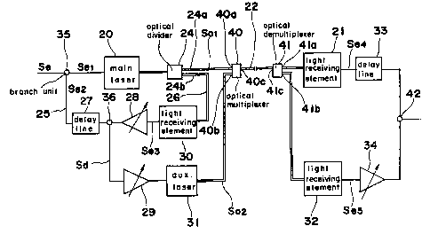
The optical communication system shown in Fig. 2
basically comprises a main semiconductor laser 20 for
generating optical signal by amplitude-modulating the
carrier light of the laser 20 in response to the amplitude
of analog signals to be transmitted (referred to as the
transmission signal hereinafter), an optical fiber line 22
for transmitting the amplitude-modulated optical signal, and
. .
, ~
~ 132869~ : -
- 6 -
a light receiving element 21 for reproducing the optical
signal transmitted by the optical fiber line 22 as an
electric signal. As the main semiconductor laser 20, there
is used a semiconductor laser of the Fabry-Perot type with
an isolator, oscillating at a wavelength ~1, such as 1.3 ~m;
and as the light receiving element 21, a PIN photo diode -
made of In Ga As is used. Between the optical fiber line
22 and the main semiconductor laser 20 there are disposed
an optical divider 24 which branches a part of the optical
signal generated from the main semiconductor laser 20 at a
port 24b connected to a branch line 26 and an optical
multiplexer 40 for applying the distortion signal So2 to
the line 22.
Between the line 22 and the light receiving element 21, -
lS there is provided an optical demultiplexer 41 for branching
the distortion signal So2 in the ~2 band from the main
signal in the ~1 band, both having been transmitted by the
line 22.
A transmission signal branch unit 35 for branching a
part of the input electrical signal is provided on a line ~ -
that connects the input port to the main semiconductor - --
laser 20. The unit 35 is also connected to a branch line - ;
25. A delay line 27 is provided on the line 25 and feeds ;~
to a subtracting point or combiner circuit 36. On the
optical signal branch line 26, there are a light receiving ^
element 30 for converting the optical signal fed from the
optical divider 24 into an electric signal Se3 representing
the transmission signal and the distortion signal, which ~;
includes the higher order harmonic signals, and an amplifier
28 of variable gain type for amplifying the signal from the
element 30. As the element 30, a PIN photo diode made of
In Ga As is used. The output terminal of the amplifier 28
is connected to the combiner 36. The combiner 36 performs
a substraction between the signal from the delay line 27
and the output signal of the amplifier 28, after the phases -
of the signals have been adjusted to coincide with each
'': ':
7 132869~
other by the delay line 27, and the amplitudes of the
signals have been adjusted to coincide with each other by
the amplifier 28, thus producing an electric signal Sd
representing the higher order harmonic distortion
components generated in the amplitude-modulation performed -
in the main semiconductor laser 20. An amplifier 29 of
variable gain type is connected to the output terminal of
the combiner 36 and the OUtpllt of the amplifier 29 is
connected to a semiconductor laser 31 (referred to as
correction laser). As the correction laser 31, there is
used a DFB semiconductor laser that generates light of
wavelength ~2 for example 1.54 ~m. The laser 31 generates
a distortion signal or correction light signal, which is an
amplitude-modulated optical signal corresponding to the
output of the amplifier 29. The distortion signal So2 is
applied to the optical fiber line 22 through the optical
multiplexer 40.
The optical demultiplexer 41 connected to the line 22
branches the distortion signal of wavelength ~2 to a light
receiving elèment 32. As the element 32 there is used a
PIN photo diode made of In Ga As which converts the
distortion signal of ~2 into an electric signal Se5. This
signal corresponds to the higher order harmonic distortion
component mentioned above. An amplif~er 34 is connected to
25 the output of the element 32. The light receiving element `
21 is connected to the output terminal of the demultiplexer
41 which outputs the main signal of the wavelength of ~1,
and the element 21 outputs an electric signal Se4
corresponding to the main signal Sol. A delay line 33 is
connected to the output of the element 21. The delay line
33 and the amplifier 34 are connected to a combiner 42. In -
the combiner 42 the electric signal corresponding to the
main signal and the electric signal corresponding to the ---
higher order harmonic distortion components are synthesized,
after adjustment in terms of phase and amplitude, so that
the modulation distortion that occurs during amplitude
.'`:,~, : ' ' '
: 1 3 2 8 6 9 ~ ~ ~
modulation in the main semiconductor laser 20 can be
eliminated.
As the multiplexer 40 and demultiplexer 41, it is
desired to use an optical fiber coupler having optical
multiplex and demultiplexing properties, such as shown in
Fig. 3. In Fig. 3, the property I shown by a solid line --
can be obtained between ports 40a and 40c of the -~
multiplexer 40 and 41a and 41c of the demultiplexer 41, for
transmission of the optical signals in the 1,3 ~m band,
while the property II shown by a dotted line can be
obtained between the ports 40b and 40c of the multiplexer
40 and 41b and 41c of the demutliplexer 41 for transmission
of the optical signals in the 1,55 ~m band. AS the optical -`
fiber coupler mentioned above, there can be used such an -~
optical fiber coupler as is disclosed in a publication
entitled ~RECENT OPTICAL FIBER COUPLER TECHNICS~ in - ~-
~OPTRONICS" vol. 5 pages 125 to 126. This optical fiber :~
coupler can be made to have an insertion loss less than 1 -~
dB for light wavelengths 1.3 ~m and 1.55 ~m. Therefore,
the CN ratio at the output of the combiner 42 is not ~
deteriorated. ~. `
Operation of the embodiment shown in Fig. 2 is as
follows:
The transmission signal Se is branched into two analog --
signals Sel and Se2 by the unit 35. The analog signal Sel
drives the main semiconductor laser 20 and is converted
into an amplitude-modulated optical signal in the 1.3 ~m
band. A part of this optical signal is taken out by the
divider 24 and is converted into the electric signal Se3 by - -
the element 30. The analog signal Se2 from the branch unit
35 is applied to the delay line 27 and the phase of the ~-
signal Se2 is adjusted to coincide with the phase of the -
output signal of the amplifier 28 applied to the combiner
36. The signal Se3 is applied to the amplifier 28 and the
amplitude of the signal Se3 is adjusted to coincide with
the amplitude of the output signal of the delay circuit 27
applied to the combiner 36. Signals Se2 and Se3 are
1328695
g
substracted, whereby the electric signal Sd corresponding
to the harmonic distortion components generated in the main
semiconductor laser 20 is formed. The signal Sd is
amplified by the amplifier 29, and then drives the
semiconductor laser 31 to generate the distortion signal
So2 which is the amplitude-modulated optical signal in the
1.55 ~m band modulated by the distortion. The distortion
signal So2 is applied to the line 22 through the ~ -
multiplexer 40 and is transmitted thereby. The main signal
Sol from the divider 24 is transmitted by the same line 22.
The distortion optical signal So2 transmitted by the ~-
line 22 is separated by the demultiplexer 41 and transmitted
to the correcting light receiving element 32, whereby the
distortion signal So2 is converted into the electric signal
Se5 representing the distortion by the element 32. The
main signal Sol transmitted by the line 22 is converted
into the electric signal Se4 by the light receiving element
21. The signals Se4 and Se5 are, after their phases and
amplitudes have been adjusted by the delay line 33 and the
amplifier 34, summed by the combiner 42 to eliminate the
modulation distortion, whereby the original analog signal
Se without the modulation distortion can be reproduced.
In this embodiment the optical fiber line 22 is a
conventional single mode, optical fiber for use with 1.3 ~m
and 10 km long. The main semiconductor laser 20 was
modulated by a sine wave of 70 MHz, whereby it was possible
to decrease by 10 dB the modulation distortion of the
secondary harmonic component of 140 MHz, compared to a case
in which the feed forward system was not used. When the
optical fiber line 22 was placed in a constant temperature
bath, changing the temperature in the range from -40C to
+85C produced a variation of the secondary order
harmonic component smaller than 1 dB at the combiner 42.
This is because, since the mzin signal and the distortion
signal are transmitted by the same optical fiber line 22, -~
the effect of the change of temperature acts on both the ~
:
132869~ ; ~
- 1 0 -- ' "' ` '
...... .
main signal and the distortion signal substantially
equally, the difference between the main signal and the
distortion signal in terms of phase and amplitude being -
almost equal.
In view of this effect, the present invention in which
the main signal and the distortion signal are transmitted
in the same optical fiber line is superior to the prior art ~
system in which the main signal and the distortion signal -
are transmitted by separate optical fiber lines. ;
The present invention is not limited to the embodiment
described above, but can be modified in various ways. For
example, in order to adjust the phase and amplitude of the
signals applied to the combiners 36 or 42, there may be
used a combination of a phase adjusting circuit and an
amplitude adjusting circuit in the respective input - -
circuits of the combiners 36 and 42.
In addition, as the optical multiplexer and/or demulti-
plexer there may be used an optical coupler of 1.3 ~m
wavelength range with a 50 ~ split ratio as shown in Fig.
4, if an attentuation of the signal of about 6 dB can be
accepted.
For example, although in the embodiment mentioned
above, the wavelength Al of the light of the main laser for
the main signal is different from the wavelength A2 of the
~5 correction laser for the distortion signal, semiconductor
lasers that generate light of the same wavelength band can
be used. However, in this case it is necessary to use an -
optical multiplexer and demultiplexer that separates
optical signals of similar wavelengths. -
~--~ ,: - . -.. . , , . ,, .. ,,-; . . .