Note: Descriptions are shown in the official language in which they were submitted.
1 328899
,
,
... .
:.
~ - 1 - 41PR-6630
: .
MOLDED CASE CIRCUIT BREAKER
MULTIPLE ACCESSORY UNIT
.....
'~ BACKGROUND OF THE INVENTION
The trend in the circuit protection industry
is currently toward complete circuit protection which
~- is accomplished by the addition of supplemental
protection apparatus to standard overcurrent
~i
' protective devices, such as molded case circuit
breakers. In the past, when such auxiliary protection
apparatus or other circuit breaker accessories were
combined with a standard circuit breaker, the
accessories were usually custom-installed at the point
of manufacture. The combined protective device, when
later installed in the field, could not be externally
accessed for inspection, replacement or repair without
destroying the integrity of the circuit breaker
. 15 interior. An example of one such factory installed
~, circuit breaker accessory is found in U.S. Patent No.
~, 4,297,663, issued October 27, 1981 to Seymour et al,
entitled "Circuit Breaker Accessories Packaged in a
Standardized Molded Case".
A more recent example of a circuit breaker
including additional accessories is found in U.S.
Patent No. 4,622,444, issued November 11, 1986 to
, . .
, ~ , ,
r
. .
- 2 - 41PR-6630
~: 1 328899
.
Kandatsu et al, entitled "circuit Breaker Housing and
Attachment Box" which allows the accessories to be
field-installed within the circuit breaker without
interfering with the integrity of the circuit breaker
~ 5 internal components. This is accomplished by mounting
`~ the accessories within a recess formed in the circuit
breaker enclosure cover.
An electronic trip actuator which is mounted
within the circuit breaker enclosure is described
within U.S. Patent No. 4,679,019, issued July 7, 1987
'J~ to Todaro et al, entitled "Trip Actuator for Molded
Case Circuit Breakers". The circuit breaker actuator
responds to trip signals generated by an electronic
.:.,
trip unit completely contained within a semiconductor
-- 15 chip such as that described within U.S. Patent No.
, 4,589,052, issued May 13, 1986 to Dougherty. The
. development of a combined trip actuator for both
^~ overcurrent protection as well as accessory function
- is found within U.S. Patent No. 4,700,161, issued
October 13, 1987 to Todaro et al, entitled "Combined
Trip Unit and Accessory Module for Electronic Trip
- Circuit Breakers". The aforementioned U.S. patents
represent the advanced state of the art of circuit
protection devices.
A shunt trip accessory unit allows the
~ circuit breaker operating mechanism to be articulated
-;~ to separate the circuit breaker contacts, usually to
perform a tripping function for electrical system
~ control and protection. One such shunt trip accessory
-~ 30 unit is described with Morris et al Canadian
Application S.N. 584,740, filed December 1, 1988,
entitled "Molded Case Circuit Breaker Shunt Trip
Unit". An auxiliary switch accessory unit allows an
operator to determine the "ONI' or "OFF" conditions of
a molded case circuit breaker contacts at a remote
:
i,
" ~
! ''
:,
,,
. i~.
- - 3 - 41PR-6630
`: 1 32~899
.
location by means of an audible alarm of visible
display. One such auxiliary switch unit is descriped
within Yu et al Canadian Application S.N. 584,739,
filed December 1, 1988, entitled "Molded Case Circuit
~ 5 Breaker Auxiliary Switch Unit".
`~ One example of an undervoltage release
circuit is found within United ~ingdom Patent
. Application 2,033,177A, entitled "Circuit Breaker with
Undervoltage Release". The circuit described within
this application applies a large initial current pulse
to the undervoltage release coil to drive the plunger
against the bias of a powerful compression spring and
uses a ballast resistor to limit the holding current
to the undervoltage release coil to a lower value. It
is believed that the heat generated within this
circuit would not allow the circuit to be contained
~.
within the confines of the circuit breaker enclosure.
- Earlier undervoltage release circuits
required different undervoltage release coils when
used within different voltage-rated circuits. This in
tuxn required inventory of a number of different coils
and custom circuits for each undervoltage application.
, -:
One purpose of the instant invention is to
provide a single undervoltage coil and circuit design
over a wide range of circuit voltage.
SUMMARY OF THE INVENTION
An integrated protection unit which includes
overcurrent protection along with auxiliary accessory
function within a common enclosure contains an
~- 30 accessory cover for access to the selected accessory
components to allow field installation of the
accessory components prior to connecting the
integrated protection unit within an electric circuit.
A multiple accessory unit which includes an
overcurrent trip coil along with an additional coil
:`
,: ~
,,~
- 4 - 41PR-6630
~ 1 32889~
that provides shunt trip or undervoltage release
~' functions is arranged within one part of the enclosure
while a printed wire board and electric switch are
~, arranged within a different part thereof. An
~,,; 5 additional printed wire board is required to provide
-~ the shunt trip function.
~.,r BRIEF DESCRIPTION OF THE DRAWINGS
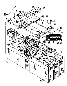
`' Figure 1 is a top perspective view of an
integrated molded case circuit breaker containing
'~ 10 selected accessory functions;
Figure 2 is an exploded top perspective view
of the integrated circuit breaker of Figure 1 prior to
~; assembly of the accessory components;
Figure 3 is an exploded front view of the
: 15 auxiliary switch and accessory electronics enclosure
, of Figure 2 prior to assembly;
Figure 4 is a schematic representation of an
undervoltage release circuit on the printed wire board
depicted in Figure 3;
Figure 5 is a schematic representation of a
shunt trip circuit on the printed wire board depicted
, in Figure 3; and
Figures 6, 7, 8 are diagrammatic
representations of combined undervoltage release and
- 25 shunt trip circuits on the printed wire board depicted
in Figure 3.
~' DESCRIPTION OF THE PREFERRED EMBODIMENT
;, An integrated circuit breaker 10 consisting
. of a molded plastic case 11 with a molded plastic
30 cover 12 is shown in Figure 1 with the accessory cover
13 attached to the circuit breaker cover. The circuit
. .~,
- breaker operating handle 18 extends up from an access
slot 19 formed in the cover escutcheon 20. A pair of
accessory doors 16, 17 are formed in the accessory
35 cover for providing access to the combined
'~f
~: .
r
':
'y:
:~'
.
. - 5 - 41PR-6630
1 328899
electromagnetic actuator and multiple accessory unit,
hereafter "actuator-accessory unit" 34 contained
within the recess 44, shown in Figure 2. Still
referring to Figure 2, the rating plug 21 is fitted
within a recess 25 formed in the accessory cover and
the accessory cover 13 is fastened to the circuit
: breaker cover by means of screws 14. The
; actuator-accessory unit is described in U.S. Patent
. No. 4,6411,117, issued February 3, 1987 to Willard,
and contains a plunger 42 for interrupting the circuit
breaker operating mechanism (not shown). The
~- operating mechanism is similar to that described with
Castonguay et al Canadian Application S.N. 573,837,
filed August 4, 1988, entitled "Molded Case Circuit
Breaker Latch and Operating Mechanism Assembly". The
actuator-accessory unit includes a flux shift coil 39
which connects with an electronic trip unit 9 on the
printed wire board 22 by means of wire conductors 38,
.. and an accessory coil 37 which connects with the
. 20 auxiliary switch-electronics enclosure 29 by means of
~,r,; wire conductors 40. The trip unit 9 on the printed
? wire board 22 is inserted in the printed wire board
' recess 23 formed in the circuit breaker cover 12 which
connects electrically with the rating plug 21 by means
~ 25 of pins 24 upstanding on the printed wire board and
.~ sockets 26 formed in the bottom of the rating plug
21. The rating plug is described in Morris et al
Canadian Application S.N. 562,397, filed March 24,
1988, entitled "Rating Plug Enclosure for Molded Case
30 Circuit Breakers. Access opening 8 formed on the top
of the rating plug 21 allows for verifying the trip
-~ characteristics of the electronic trip unit 9. The
; electronic trip unit electrically connects with a
., current transformer (not shown) contained within the
35 integrated circuit breaker case 11 and which is
o
s
i~
- 6 - 41PR-6630
r 1 3 2 8 8 9 9
described in U.S. Patent No. 4,591,942, issued May
27, 1986. The integrated circuit breaker 10
depicted in Figure 1 includes three poles, with one
current transformer supplied within each separate
pole. Still referring to Figure 2, in accordance
with the instant invention, the auxiliary switch and
accessory electronics enclosure 29, hereafter
"switch-electronics enclosure" is inserted within a
recess 30 formed in the integrated circuit breaker
cover 12 and is positioned such that a depending
operating lever 33 interacts with the circuit
breaker operating mechanism in a manner to be
described below in greater detail. Wire conductors
31, 31' electrically connect with a remote voltage
source (not shown) through a wire access slot 32
formed in the case 11 to articulate the circuit
breaker operating mechanism to separate the circuit
~` breaker contacts by either a shunt trip or
;~ undervoltage release function in a manner to be
described below in some detail. The wire conductors
31 connect with an external voltage source to the
undervoltage release electronics and the wire
~.~
conductors 31' connect an external voltage source to
the shunt trip electronics (not shown). In the
~5 particular arrangement depicted in Figure 2, access
to the actuator-accessory unit 34 is made by means
of accessory door 16 which is integrally formed
~, within the accessory cover 13 and access to the
switch-electronics enclosure 29 is made by means of
;~ 30 accessory door 17. This arrangement differs from
` that described in Yu et al Canadian Application S.N.
584,739, filed December 1, 1988, entitled "Molded
:~ Case Circuit Breaker Auxiliary Switch Unit" which
does not provide undervoltage release or shunt trip
functions and Morris et al Canadian Application S.N.
584,740, filed December 1, 1988, entitled "Molded
,
, . .~.
7 _ 41PR-6630 1 3288q9
:
Case Circuit Breaker Shunt Trip Unit" which does not
provide an undervoltage release function. The
accessory doors 16, 17 are hingably attached to the
accessory cover 13 by means of a hinge 15 integrally
formed therein and the accessory door is then fastened
to the circuit breaker cover by means of screws 14,
thru hole 27 formed in the accessory door, and
threaded openings 28 formed in the circuit breaker
cover. A good description of the accessory cover 13
is found within Raymont et al Canadian Application
S.N. 522,395, filed March 24, 1988 and entitled
~ "Molded Case Circuit Breaker Accessory Enclosure".
i, In an earlier combined actuator-accessory
unit described in U.S. Patent No. 4,706,158, issued
15 November 10, 1987 to Todaro et al, entitled "Circuit
Breaker with Self-Contained Electronic Trip Actuator
and Undervoltage Release Control Circuit" the
electronics for controlling the trip actuator, shunt
trip and undervoltage release coils were contained on
separate printed wire boards contained in a common
unit with the flux shift and undervoltage release
coils. In the actuator-accessory unit 34 of the
~ instant invention, which is similar to that described
-~ in the aforementioned U.S. Patent No. 4,641,117, the
flux shift coil 39 and the accessory coil 36 are
intentionally separated fro the accessory
electronics. The accessory electronics for
-- controlling the actuator-accessory unit 34 of this
invention are contained within a pair of printed wire
30 boards 61, 68 (Figure 3) containing circuits depicted
in Figures 4-8 which will be discussed below in
greater detail. In operating the shunt trip aspect of
the actuator-accessory unit, which involves the
~ plunger 42, compression spring 43, magnetic diverter
- 35 85, magnetic conductor 41, flux shift coil 39 and
....
~`
r
- 8 -- 41PR-6630
1 32889q
permanent magnet 36 all contained within a metallic
casing 35, the permanent magnet 36 holds the plunger
42 against the bias provided by the charged
compression spring 43 in the absence of any voltage
. 5 applied to the flux shift coil 39 over wire conductors
38. Upon the occurrence of an over-current condition,
a voltage applied to the wire conductors 38 via the
printed wire board 22 energizes the flux shift coil 39
~ which generates a magnetic field in opposition to the
.. 10 magnetic field supplied by the permanent magnet 36 and
diverts the magnetic field of the permanent magnet to
. the casing 35 via the magnetic diverter 85. The
' plunger 42 is then rapidly propelled in the forward
indicated direction by the bias provided by the
charged compression spring 43 to interact with the
circuit breaker operating mechanism, as described
: earlier. When the actuator-accessory unit 34 includes
A` an undervoltage-release accessory function, the
accessory coil 37 is an undervoltage release coil and
the permanent magnet 36 is absent such that the
magnetic holding force provided to the plunger 42, via
~-i. magnetic conductor 41, i5 supplied by the flux
- ,;
-:: generated by the undervoltage release coil 37,
;. per se. When the voltage supplied to the wire
.-^. 25 conductors 38 via the switch-electronics enclosure 29
~ decreases to a predetermined value for a predetermined
:~ period of time, the magnetic force applied to the
plunger is insufficient to hold the plunger against
-.~ the bias of the charged compression spring 43 and the
plunger becomes propelled in the indicated direction
to articulate the circuit breaker operating
. mechanism. When the actuator-accessory unit 34 is
arranged as a shunt-trip accessory, the permanent
magnet 36 is present and the accessory coil 37 is a
shunt trip coil which, upon the application of a
'
. - 9 - 41PR-6630
1 32889q
;~ voltage to the wire conductors 40 via the switch-
electronics enclosure 29, generates a reverse magnetic
field to that of the permanent magnet 36, to
` substantially reduce the magnetic force provided by
~ 5 the permanent magnet 36 and thereby allow the plunger
j 42 to become propelled in the indicated direction by
the bias of the compression spring 43.
The switch-electronics enclosure 29 is
:. assembled in the manner best seen by referring now to
:,~ 10 Figure 3. An electric switch 47 is positioned within
the switch-electronics enclosure case 46 by capturing
a post 48, formed on the back wall 55 of the case,
within a thru hole 49 on the electric switch and
:~ fastening the switch to the rear wall by means of a
~; 15 rivet 50, thru hole 51 and thru hole 56. The electric
. switch is now positioned such that the plunger 60
-~ interacts with a tab 59 extending from the top
extension 58 of the operating lever 33 with the bottom
;.~ extension 86 arranged for interacting with the circuit
breaker operating mechanism. The operating lever 33
:. is pivotally arranged within a journal 53 integrally
. ~,
` formed in the bottom 54 of the case by means of the
~ pivot pin 52. The electric switch connects with a
:~ printed wire board 61 by means of a pair of wire
.~ 25 conductors 62 attached to the wire connectors 63 which
extend from the electric switch at one end and are
.: soldered to the printed wire board 61 at an opposite
end. The electric switch operates in the manner
A described within the aforementioned ~.rl~ et al
Canadian Application S.N.~ 73~. When the printed
~5 wire board 61 is inserted within the case 46, the
projection 67 formed within the case positions the
printed wire board such that a pair of edge-connector
pads 64A, 64B on the bottom of the printed wire board
, 35 are aligned with a corresponding pair of slots 65
-
:
- 10 - 41PR-6630
1 328899
formed within the extension 66 of the bottom 54 for
electrically interconnecting the printed wire board 61
with stab-connectors 93A, 93B upstanding from the
bottom of the recess 30 (Figure 2) as also described
, 5 within the aforementioned Morris et al Canadian
: A Application S.N. S~Y,73~. The stab connectors
: electrically connect with the wire conductors 40 by
means of wire slot 94 formed in the side of the recess
.. 30, as best seen in Figure 2.
. 10 Referring back to Figure 3, selection of a
, desired accessory is made by selecting the appropriate
actuator-accessory unit which contains either a shunt
trip coil or an undervoltage release coil in addition
. to the flux shift coil 39 (Figure 2) along with
. 15 selection of a corresponding switch-electronics
; enclosure 29. The shunt trip function per se is
~ provided by a circuit such as that shown at 78 in
: .~
',.~ Figure 5, contained within the switch-electronics
~ enclosure while the undervoltage function, per se is
.:~^ 20 provided by a circuit such as that shown in Figure 4,
contained within the switch-electronics enclosure.
~ For the switch-electronics enclosure 29 of Figure 3
-~ has facility for providing either undervoltage
.. ~ function per se or undervoltage function along with
. :~
-~ 25 shunt trip function when used with an
~' actuator-accessory unit which includes an undervoltage
coil. Still referring to Figure 3, the printed wire
. board 68, which is mechanically and electrically
^ connected with the printed wire board 61 by means of
plugs 69 extending from the printed wire board 61 and
sockets 70 within the printed wire board 68 contains
the shunt trip circuit 78 (Figure 5). When the
printed wire board 68 is at~ached to the printed wire
board 61, the printed wire board 68 seats within the
extension 71 arranged on the opposite side of the case
- 11 - 41PR-6630 1 328~39q
46 from the extension 66. since the accessory coil 37
within the actuator-accessory unit 34 of Figure 2 is
an undervoltage coil, as described earlier the
undervoltage circuit 72 (Figure 4) on the printed wire
board 61 controls the operation of the undervoltage
coil. The switch-electronics enclosure cover 45 is
sealed the wire conductors 31, 31' exit through
openings 92.
.`. The undervoltage circuit 72 of Figure 4
~i 10 enables the undervoltage accessory coil 37 when the
voltage across terminals T1, T2, falls below a
predetermined value for a predetermined time. An
external voltage source (not shown) is applied to
terminals T1, T2 via conductors 31 thereby providing
current through the current limiting resistor R1 and
the rectifier consisting of diodes Dl-D4 to the
.. negative bus 75. A varistor Zl is connected across
, the terminals to protect the undervoltage circuit 72
:. from voltage surges. The other output of the diode
. 20 rectifier connects with the positive bus 74. The
undervoltage release coil 37 is connected between the
positive bus 74 and the drain terminal of a FET1,
,~ the source of the FETl connects with the negative
,~ bus 75 through diode D6, and resistors R2, Rg.
. 25 A flyback diode D5 is used to circulate current back
through the undervoltage accessory coil when the
FETl is turned off. Output pin 7 of a comparator 76
.,~ connects with the gate of the FETl and input pin 6
:, of the comparator connects with the source of FET1
' 30 through resistor R3 and diode D7. The input pin 6
- connects with the negative bus 75 through capacitor
C1. The other input to the comparator 76 connects
to the midpoint of the voltage divider consisting of
~A resistors R6-Rg. The chopper circuit, consisting
essentially of the FETl and the comparator 76,
,
(
.~
- 12 - 41PR-6630
'~ 1 3288q9
controls the current to the undervoltage accessory
- coil 37 in the following manner. With the FET1 in
its "OFF" state, input pin 5 to the comparator is set
at 2 volts at the junction of resistors R7 and
-- 5 R8. When the voltage across capacitor Cl is less
than 2 volts, the output pin 7 of the comparator 76 is
"high", turning on the FETl and allowing current to
flow through the undervoltage accessory coil 37. When
~ the FETl is on, the circuit current through diode
: 10 D6, and resistor R2 develops a proportional
-~. voltage across R2 and Rg. Capacitor Cl charges
to this voltage through diode D7 and resistor R3.
, Diode D6, in series with resistor R2, provides
; both voltage and temperature compensation for diode
~'s 15 D7 while resistor R3 provides a short time delay
. during the charging cycle for capacitor Cl so that
the comparator 76 does not turn off prematurely due to
~ the occurrence of a current spike during reverse
-~ recovery of diode D5. For selected values of R2
-~ 20 and Rg at 30 milliamps circuit current, the voltage
~ dev~loped across R2 and Rg is approximately 3
^~ volts. The voltage across Rg adds to the voltage
;i; across R8 to bias input pin 5 of the comparator 76
at approximately 3 volts. When the circuit current
exceeds 30 milliamps, capacitor Cl will charge
greater than 3 volts driving the output pin 7 of the
~ comparator 76 to a "low" state, thereby turning off
- the FETl. With the FETl off, the voltage on input
pin 5 reverts back to the 2 volt reference value.
With 3 volts across capacitor Cl the output of
comparator 76 cannot go "high" until the voltage
across Cl drops to less than 2 volts. Cl can only
discharge through resistor R4 which connects the
output pin l of the second comparator 77, which is
"low". The value of resistor R4 is selected to
.
.. . .
~ 3~8899
- 13 - 41PR-6630
provide a fixed time delay for the capacitor c1 to
decay to 2 volts thereby establishing a fixed off-time
for the FET1. The circuit current through the
undervoltage accessory coil 37 is arranged to turn off
at approximately 30 milliamps. Diode D5 then
circulates the energy stored in the inductance of the
undervoltage accessory coil in order to maintain the
current at a sufficiently high value to prevent the
. .
. compression spring 43, in Figure 2, from propelling
, 10 the plunger 42 within the actuator-accessory unit 34
in the forward direction as indicated. The circuit
current through the undervoltage accessory coil decays
to approximately 20 milliamps after a predetermined
time delay which is determined by the inductive and
, 15 resistive properties of the undervoltage accessory
r,i coil 37. The resistor R4 is selected to discharge
capacitor C1 from 3 volts to 2 volts in the same
predetermined time delay. After the predetermined
time delay, the output pin 7 of comparator 76 goes
"high" causing the process just described to repeat
~ itself. If the voltage applied to terminals Tl, T2
-~ should at any time drop below a predetermined value,
the output pin 1 of the second comparator 77 will go
i~; "high" thereby charging the capacitor C1 up to the
fi' 25 positive rail voltage of the second comparator 77,
which in turn, drives the output pin 7 of comparator
, 76 "low" to turn off the FET1. When the voltage
`' across terminals T1, T2, increases, the output pin
1 of the second comparator 77 is "low" causing the
capacitor C1 to discharge through resistor R4. As
soon as the voltage across capacitor C1 decays to 2
volts, FETl turns on and the process described
earlier repeats.
Resistors R1o, R11 connecting across the
negative and positive busses 75, 74 in combination
.
"
..
:'
,
,
.
- 14 - 41PR-6630 1 328899
with the second capacitor C2, connecting across
R11, form a simple averaging circuit producing an
,~ approximately constant output voltage across C3.
-i The voltage value across C3 determines the voltage
:`~. 5 value above which circuit current is applied to the
J; undervoltage accessory coil 37 defined herein as the
"pick-up" value and below which, current to the
~; undervoltage accessory coil will be interrupted which
.~ is defined as the "drop-out" value. In operation, the
average voltage established across capacitor C2 is
applied to the input pin 2 of the second comparator 77
through a current limiting resistor R5. The current
.~ limiting resistor R5 limits the current into the
~` input pin 2 when the voltage across C2 exceeds the
:~ 15 positive rail voltage applied to the second comparator
77 at pin 8. Input pin 3 of the second comparator is
~:. set at approximately 7 volts by the voltage divider
.~ R6-R9 which determines the voltage appearing at the
connection point between R6 and R7. When the
voltage across capacitor C2 is below 7 volts, the
output pin 1 of the second comparator 77 goes "high"
causing the first comparator 76 to interrupt the
current to the undervoltage accessory coil 37.
. Conversely, when the voltage across C2 is greater
than 7 volts, the output pin 1 of the second
comparator 77 is "low" thereby applying voltage to the
gate electrode of the FETl to turn on the FETl and
allow the comparator 76 to apply current to the
undervoltage accessory coil 37. Resistor R12, zener
diode D8, transistor Ql and capacitor C3 serve
to regulate the voltage at the emitter f Ql in the
following manner. Resistor R12 and zener diode D8
establish a reference voltage for the base Of Ql
- which in turn, supplies a regulated output voltage at
. 35 the emitter f Ql which is applied to the junction
. '.
-~:
:~;
,:,
' .
- 15 - 41PR-6630 l 328899
,,
of pin 8 on the second comparator 77 and resistor
R6. Resistor R12 and the collector of a polar
transistor Q1 are connected with a storage capacitor
C4. The function of capacitor C3 is to provide RF
suppression to the base of transistor Q1 The
undervoltage circuit 72 requires a relatively low
level of steady current, in the order of 1
milliampere, to maintain operation of the electronic
devices such as FETl,FET2, comparators 76, 77 and
transistor Ql- A higher level of current, in the
order of 30 milliamps, is applied to the undervoltage
accessory coil 37 to generate sufficient magnetic flux
to hold the plunger 42 of Figure 2 against the charged
compression spring 43. The 30 milliampere current to
the undervoltage accessory coil must be maintained
while the AC voltage applied to terminals Tl, T2
passes through its zero crossing on each half of the
AC cycle. This is accomplished by the combination of
FET2 with resistor R13 and storage capacitor
C4. Resistor R13, in series with zener diode
D1o, establishes a 30 volt gate reference voltage at
the drain electrode of the FET2 which sets a charge
level of 30 volts for the storage capacitor C4
connected to the junction of zener diode Dg,
resistor R12 and the collector of transistor Ql
When capacitor C4 is less than 30 volts and the AC
voltage applied to terminals Tl, T2 is greater than 30
volts, the gate electrode of FET2 is positive with
respect to the source electrode such that FET2
applies charging current to the storage capacitor
i.~
^~ C4. As C4 approaches 30 volts, FET2 turns off
to apply the low level steady current requirements
described earlier. Accordingly, zener diode Dg
protects the gate 8 of FET2 from overvoltage
3S conditions in the event that the AC voltage is applied
` - 16 - 41PR-6630
1 328899
'~ to terminals T1, T2 when the capacitor C4 is
completely discharged. With capacitor C4 fully
charged, high ambient temperature could cause leakage
current in the FET2 to increase the charging voltage
applied to the storage capacitor C4, in excess of
~, the rate value of the capacitor. The zener diode Dg
, functions to limit the voltage applied to the storage
capacitor C4 to one diode-voltage above the voltage
-~ across the zener diode Dlo. Zener diode Dg
accordingly supplies a negative voltage to the gate
electrode of the FET2 to reduce the FET2 leakage
r~ current and thereby protect the storage capacitor C4
from excess voltage. As described earlier, the
storage capacitor C4 provides energy to the
undervoltage accessory coil 37 when the voltage
applied to terminals Tl, T2 drops below the 30 volt
level. The discharge path for the storage capacitor
C4 is through the internal source-drain diode of
FET2, the undervoltage accessory coil 37 through
FETl, diode D6, resistors R2, Rg and back
through the storage capacitor C4.
The undervoltage release circuit of the
instant invention substantially improves over
conventional RC energy storage circuits because of its
low power dissipation at high input voltages thereby
allowing the highly beneficial use of smaller size and
lower rated storage capacitors. Low power dissipation
is provided by the FET2 in circuit with the storage
, capacitor C4 whereby capacitor C4 is charged
;~ 30 through operation of FET2 only during the rising
part of the wave form of the AC voltage applied across
input terminals T1, T2 typically between 30-80 volts.
The FET2 remains off until the voltage again drops
to less than 30 volts. Since the peak voltage
appearing across the input terminals Tl, T2 can exceed
:~'
:-'
- 17 - 41PR-6630 1 328~q9
:,
;~ 350 volts, charging the storage capacitor C4 at the
'~ lower voltage level is an important feature of the
instant invention.
The shunt trip circuit 78 within the printed
wire board 68, (Figure 3) is depicted in Figure 5 and
~-~. contains the following components. Terminal T3
~. ~
connects through a current limiting resistor R1 to
one input of a bridge rectifier consisting of diodes
" 't D1-D4 to provide positive potential to a positive
'~ 10 bus conductor 90. Terminal T4 connects through
electric switch 47 to the other input to the bridge
rectifier. A voltage suppressing varistor Zl is
connected across the inputs to the bridge rectifier to
protect the circuit 78 from excess voltage gradients.
~, 15 One output of the bridge rectifier connects through
resistor R2 with the positive bus 90 which
~; terminates at the printed wire board edge-connector
~; pad 64A. The other output of the bridge rectifier
connects to the negative bus 91 and from there through
a silicon bilateral switch SC1 to the other
edge-connector pad 64B. A storage capacitor C1 is
connected across the positive and negative busses 90,
91 and becomes charged by the voltage applied across
terminals T3, T4. When the voltage on capacitor C1
is greater than the break-over voltage of the silicon
bilateral switch SC1, the capacitor C1 discharges
~,~ through the accessory coil 37 arranged as a shunt trip
coil to articulate the circuit breaker operating
mechanism as described in the aforementioned U.S.
:~ 30 Patent No. 4,700,161. A resistor R3 bleeds off
current from capacitor C1 allowing the circuit
' breaker operating mechanism to be reset. Diode D5
' connected across the accessory coil 37 protects the
coil from excess voltage during a shunt trip
operation. The electric switch 47 located within the
: .
, i .
:,,
,
- 18 - 41PR-6630
1 328899
switch-electronics enclosure 29 best seen by referring
to Figure 3, protects the shunt trip accessory coil 37
~, from overheating by immediately disconnecting voltage
to the printed wire board 68 as soon as the circuit
breaker operating mechanism has responded. This is
accomplished by the interaction of the bottom
extension 86 of the operating lever 33 with the
- circuit breaker operating mechanism (not shown). The
bottom extension of the operating lever holds the top
extension 58 and angled tab 59 in contact with the
electric switch plunger 60 as long as the bottom
extension 86 remains in contact with the circuit
breaker operating mechanism. When the shunt trip
accessory coil 37 has articulated the circuit breaker
- 15 operating mechanism, the bottom extension 86 of the
operating lever 33 moves away from the electric switch
plunger 60 allowing the plunger to extend and
interrupt circuit through the switch 47 to immediately
interrupt the voltage applied to the printed wire
boards 61, 68 and hence to the shunt trip accessory
coil 37 to prevent the shunt trip accessory coil from
~' overheating. When the circuit breaker operating
mechanism is turned on, the bottom extension 86 moves
, back into contact with the plunger 60 causing the
.~,
~`$ 25 electric switch 47 to close and restoring charging
power to the storage capacitor C1 of Figure 5. The
undervoltage release circuit 72 (Figure 4) is
` contained on the printed wire board 61 of Figure 3
whereas the shunt trip circuit 78 (Figure 5) is
contained on the printed wire board 68. The external
wire conductors 31' which control the shunt trip
circuit 78 are shown in phantom in Figure 3 to
distinguish from the solid external wire conductors 31
which control the undervoltage release circuit 72.
A combined undervoltage release and shunt
.:,
.,
~'
.
- 19 - 41PR-6630
1 328899
i~: trip control circuit 79 is shown i Figure 6 wherein a
, common accessory coil 37 provides both undervoltage
release and shunt trip functions. A first set of
, input terminals T1, T2 provides operating voltage to
~- 5 an undervoltage control circuit 72 such as that
, described earlier with reference to Figure 4 and which
connects with one leg of the combined undervoltage-
~ shunt trip coil 37 through a current limiting resistor
s` R14 and connects directly with the other leg. The
shunt trip control circuit 78, such as described
earlier with reference to Figure 5, connects with the
. combined undervoltage release and shunt trip coil 37
hereafter "combined accessory coil" by means of an
opto-isolator 73. The opto-isolator includes a light
:~ 15 emitting diode Dl which connects with the shunt trip
~, control circuit 78 over conductors in combination with
.; a photo transistor Q1 The collector and emitter of
. the photo transistor connector directly with the two
legs 40 of the combined accessory coil 37. Both
.~ 20 undervoltage release and shunt trip functions are
~ obtained by applying the external power to input
.~, terminals Tl, T2 to continuously energize the combined
accessory coil 37 until an undervoltage condition is
~~ processed within the undervoltage control circuit 72
~, 25 whereby the current to the combined accessory 37 is
.,. interrupted to allow the plunger 421 to become
~, extended under the bias provided by the charged
~ compression spring 43 within the actuator-accessory
"f; unit 34 (Figure 2). The opto-isolator 73 prevents
electrical interaction between the undervoltage
' control circuit 72 and the shunt trip control circuit
.Y 78. To operate the combined accessory coil 37 for
, shunt trip operation, a voltage is applied to the
. shunt trip control circuit 78 by means of terminals
T3, T4. The opto-isolator 73 shunts a current
,,~
- 20 - 41PR-6630 1 3288 99
supplied from the undervoltage control circuit 72 away
from the combined accessory coil 37. This immediately
causes the magnetic force on the plunger 42 to
decrease to a value less than the holding force
required to maintain the plunger 42 against the bias
exerted by the charged compression spring 43 thereby
; projecting the plunger 42 forward as indicated.
An alternate combined accessory circuit 80
- is depicted in Figure 7 wherein the opto-isolator 73
of Figure 6 is replaced by an electromagnetic relay
82. The electromagnetic relay is normally "open"
whereby the relay contacts 84 across the legs 40 of
the combined accessory coil 37, are not connected
together. Upon application of a voltage to the input
terminals T3, T4 to the shunt trip control circuit 78,
current is provided through the winding 83 of the
electromagnetic relay 82 thereby connecting the
.: contacts 84 and shorting the current applied to the
., .
combined accessory coil 37 provided by the
;~ 20 undervoltage control circuit. The plunger 42 within
'"'`r' the actuator-accessory unit 34 of Figure 2 responds in
~ the manner described earlier with reference to
-~ Figure 6.
A further embodiment of a combined accessory
circuit 81 is depicted in Figure 8 with the normally
;~ "open" relay 82 of Figure 7 replaced with a normally
"closed" relay 82'. The undervoltage control circuit
72 connects directly with one leg of the combined
accessory coil 37 and connects with the other leg
through the closed contacts 84' in series with the
undervoltage release control circuit 72. A voltage is
;~` applied to the input terminals T1, T2 to the
undervoltage control circuit 72 and provides a holding
:
current through the combined accessory coil 37 through
the closeù contacts 84'. When a shunt trip functlon
,
- 21 - 41PR-6630 1 328899
is to e performed, a voltage is applied to the input
terminals T3, T4 to the shunt trip control circuit 78
activating the electromagnetic relay 83' and opening
the normally closed contact 84'. This interrupts the
holding current to the combined accessory coil 37
causing the plunger 42 within the actuator-accessory
unit 34 of Figure 2 to extend as described earlier for
the circuits of Figures 6 and 7.
.,,
:;,
;`
.
-;
.:
'~
:~
. ,.
;,....
; r.,
;
,~i,
~ r
.','~
'`~,
, :i
. ~
~,