Note: Descriptions are shown in the official language in which they were submitted.
1328984
SPECIFICATION
DETAILED DESCRIPTION OF THE INVENTION
[Field of the Invention]
The present invention relates to a method of producing
a superconducting wire, in particular to a method of producing
a æuperconducting wire capable of obtaining a ceramics
superconducting wire having a high critical temperature.
[Prior Art]
The superconducting wire has been produced by turning a
metallic superconductor (alloys, such as NbTi, and
intermetallic compounds, such as Nb2SN and V3Ga) into a wire.
However, their critical temperature (Tc) is 30K or less, so
that they are poor in practical use. Accordingly, a
superconductor having a high critical temperature has been
desired.
And, a ceramics superconductor having a critical
temperature of 30K or more has been recently developed.
[Problems to be Solved by the Invention]
However, the above described ceramics superconductors
have exhibited problems in that the workability is remarkably
lowered due to the poor ductility and flexibility, so that
they are very difficult to turn into a wire, and the
constituent elements other than elements of the group IIa in
the periodic table, elements of the group IIIa in the periodic
table, copper and oxygen, which enter superconducting
.. ;,,- ,- ' . , ' . .: .. -
, "
.: .: ,
. : ~
.,,.,~, . ~ - , . .: : ,
~ :, . . . . . .
.: .
:-. : ,
`` 1328984
materials as impurities when sintered at high temperatures
after giving a desired shape to them to obtain such ceramics
conductors, have a bad influence upon superconducting
characteristics such as critical temperature according to
circumstances.
[Ob~ect of the Invention]
The present invention was achieved in view of the above
described problems.
It i8 an object of the present invention to provide a
method of producing a superconducting wire in which there is
not the possibility of having a bad influence upon
superconductingcharacteristics and aceramics superconducting
wire having a high critical temperature can be obtained.
[Measures for Solving the Problems]
i In order to achieve the above described object, according
to a method of producing a superconducting wire of the present
invention, a ceramics superconducting material is coated with
Cu-Be alloys and then turning into a wire material having an
appointed shape followed by sintering said wire material at
a temperature range, at which a superconducting layer can be
formed, to obtain a superconducting wire with the
superconducting layer coated with said alloys.
[Operation]
According to a method of producing a superconducting wire
'! having the above described construction, the Cu-Be alloys have
.
~; (2)
~-~ r '
. ~,..
:;. : .~ . :
~''` ' . ~1 ' ' . :
'": : ' '.' ~ ~ '' "''''
.: ~
ir ~
, ~ ~
`-~ 132898~
a large ductility and a sufficient strength capable of
standing up to the area-reduction processing, so that an
outside force due to the processing in the area-reduction
processing can be effectively transmitted to the internal
superconducting material through the Cu-Be alloys as the
coating, whereby the desired wire material can be obtained.
In addition, both Cu and Be can be elements composing the
superconducting material, so that even though Cu and Be are
diffused from the coating to enter the superconducting
material when the wire material is sintered, there is not the
possibility of having a bad influence upon the superconducting
characteristics of the resulting superconducting wire.
',
; [Preferred Embodiment]
Next, one preferred embodiment of the present invention
is described with reference to the drawings.
Fig. lA to C is a sectional view showing respective
processes, in which a superconducting wire is obtained
according to a method of the present invention; and
Fig. 2 is a sectional view showing an application example
`~ of a superconducting wire.
;
At first, a powdery mixture of a ceramics superconducting
material (2) is filled in a cylindrical pipe formed of Cu-Be
alloys (3) to obtain a double-layer material (hereinafter
referred to as non-processed wire material) with the
superconducting material (2) coated with the Cu-Be alloys (3),
~A, as shown in Fig. lA.
,~
,.
~ (3)
"~
'~1
~ X
,.. : . , ~, :
:,~ . - . ,; ~, .. :
,: :
.,.,.~ ~ ' " ~
... , . . ~
:`;
1328984
Every material containing elements composing the
superconducting material can be used as said superconducting
material (2) regardless of elements and compounds. Said
elements include elements of the groups I, II and III in the
periodic table, oxygen, nitrogen, fluorine, carbon, sulfur and
the like. In particular, said superconducting material (2)
include at least one element selected from the group
consisting of elements of the group Ia, elements of the group
IIa and elements of the groups IIIa in the periodic table, at
least one element selected from elements of the group Ib,
elements of the group IIb and elements of the group IIIb in
the periodic table, and at least one element selected from the
group consisting of oxygen, nitrogen, fluorine, carbon and
sulfur. Of the above described elements of the group I in the
periodic table, the elements of the group Ia include Li, Na,
K, Rb, Cs, Fr and the like and the elements of the group Ib
include Cu, Ag and Au. In addition, of the elements of the
group II in the periodic table, the elements of the group IIa
include Be, Ng, Ca, Sr, Ba and Ra and the elements of the
group IIb include Zn, Cd and the like. Of the elements of the
group III, the elements of the group IIIa include Sc, Y,
lanthanoid elements, such as La, Ce, Pr, Nd, Pm, ~m, Eu, Gd,
Tb, Dy, Ho, Er, Tm, Yb and Lu, actinoid elements, such as Ac,
and the like. Besides, the elements of the group IIIb include
Al, Ga, In, Tl and the like.
Of the above described elements, the elements selected
from the group consisting of the elements of the group Ib, the
elements of the group IIa, the elements of the group IIIa,
(4)
' .~,
I .
,.,, ~ . : :
. : '
i.;,: . .
,,
~.,
:
-` 132~9~
lanthanoid elements and oxygen are preferably used. In
addition, of the elements of the group Ib in the periodic
table, Cu is in particular preferably used. In addition, of
the elements of the group IIa in the periodic table, Sr, Ba
and Be are preferably used. Of the elements of the group IIIa
in the periodic table, Sc, Y and La are preferably used.
The above described elements themselves or compounds
containing the above described elements are used singly or in
combination in the form of powder and in the case where they
are used in the form of compound, chlorides, nitrides and
carbides may be used but oxides, carbonates, sulfides or
fluorides are preferably used and oxides or carbonates are in
particular preferably used. In addition, said powdery mixture
may be composed of oxides or carbonates of the above described
elements. In addition, the Cu-Be alloy (3) contains Be at a
ratio of 0.01 to 5.0 ~ by weight. The ductility and the
strength of the Cu-Be alloys is reduced and increased with an
increase of a content of Be, respectively, but if Be is
contained at the above described range, the ductility and
strength sufficient for obtaining a long wire material having
a small diameter by the area-reduction processing can be
obtained.
Subsequently, the non-processed wire material is
sub~ected to the area-reduction processing, such as extrusion,
drawing and swaging, to obtain a long wire material having a
small diameter as shown in Fig. lB.
And, the resulting long wire material having a small
diameter is sintered at a temperature range, at which the
(5)
~.
:",~
;,$~
'.~i.' , ..
1328984
superconducting layer can be formed, to obtain the ceramics
superconducting wire (1) with the superconducting layer (4)
coated with said alloys (3) as shown in Fig. lC. At this
time, the Cu-Be alloys (3) are used as the coating, so that
S elements other than Cu and Be do not diffuse from said coating
and do not enter the superconducting material. Accordingly,
there is not also the possibility of having a bad influence
upon the superconducting characteristics, such as critical
temperature, of the resulting superconducting wire (1).
In addition, if it is intended to give a strength of the
same degree as that of the Cu-Be alloys (3) by adding elements
other than Be to the general Cu alloys, it is required to add
said elements at a ratio of 10 % by weight or more. For
example, the tensile strength and elongation of an annealed
Cu-2 wt. ~ Be alloy material is 48 kg/mm2 and 35 ~,
respectively. On the contrary, the tensile strength and the
elongation of the general Cu-10 wt. % Ni alloy material is 30
kgtmm2 and 42 %, respectively, and this alloy contains Ni
which is an element belonging to the group VIIIa, so that
there is a possibility of having a bad influence upon the
superconducting characteristics. Accordingly, the Cu-Be
alloys are preferably used as the coating.
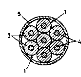
In addition, as a rule the superconducting wire (1) is
~ used with being coated with an insulting material (5). Fig.
- 25 2 is a sectional view showing one application example in which
a bundle of a plurality of superconducting wires (1) is coated
with the insulting material (5). The bundle of a plurality
of superconducting wires (1) coated with the insulating
!,
(6)
X'
".;~
,,,.
. .
~- .
" ~ ~
~ : :
,."
~32~984
material (5) is superior to one piece of superconducting wire
(1) having the same sectional area in flexibility.
In addition, a method of producing the superconducting
wire (1) according to the present invention is not limited to
S the above described preferred embodiment. For example, a
measure for obtaining the non-processed wire material, in
which a long rod having a small diameter formed of copper is
inserted into a pipe formed of the Cu-Be alloys (3) and then
the powdery mixture of the superconducting material (2) is
filled in the circumferance of said rod, may be used. In
addition, a measure, in which a powdery mixture of the
superconducting material (2) is molded in columnar shape and
the periphery of the resulting columnar molded product is
coated with the Cu-Be alloys (3), may be used. In addition,
a sectional shape of an inner circumferential surface and an
outer circumferential surface of the pipe may be oval,
rectangular and the like in addition to circular. Various
kinds of modification are possible without deviating from the
spirit of the invention.
[Experimental Example]
One experimental example of the superconducting wire
obtained by the method of the present invention is below
described.
A powdery mixture comprising Y2O3, BaCO3 and CuO charged
in a pipe of Cu-2%Be having an outside diameter of 20 mm and
an inside diameter of 10 mm was subjected to the area-
reduction processing. As a result, the powdery mixture could
(7)
!~.` .' :
/".~
.;' '.', ~ - ~: ,"
'. .~, , .' : '
.'~'~ ' '' ' '
`,: ' ~
1328984
be turned into a wire having an outside diameter of 0.5 mm
without breaking. The superconducting wire obtained by
sintering the resulting wire material for 3 hours at 900C was
measured on the critical temperature with the result of
TC=45K. If sintering condition is made best fit, Tc is
expected to further improve.
As above described, the superconducting wire having a
diameter nearly same as that of the general wire can be
obtained.
tEffeCtS of the Invention]
As above described, according to the method of producing
; a superconducting wire of the present invention, the ceramics
superconducting materials are coated with the Cu-Be alloys,
which are suitable for the area-reduction processing in
respect of ductility and strength, so that the superconducting
materials can be subjected to the area-reduction processing
to obtain the long wire material having a small diameter. The
resulting wire material can be sintered to easily obtain the
superconducting wire. In addition, the Cu-Be alloys can be
elements composing the superconducting materials, so that
special effects are exhibited in that there is not the
possibility of having a bad influence upon the superconducting
characteristics and the ceramics superconducting wire having
a high critical temperature can be obtained.
~1
i~
~ (8)
.,.~~,
:-.
. , :
.'~ ' ' .