Note: Descriptions are shown in the official language in which they were submitted.
1 330237
BACRGROUND OF THE INVENTION
Fiel~ of the Invention
This invention relates generally to video cameras and,
more particularly, is dire¢ted to an improved arrangement for
effecting automatic white balance adjustment in a video camera
system of the type having a camera body on which exchangeable lens
devices are interchangeably mountable.
'` ~ ~.' '`:
DESCRIPq!ION OF THB PRIOR ART
It is known to provide a video camera with a white
balance adjusting circuit. Such video cameras generally comprise a
lens assembly for projecting a light image on an image pick up
element which may be a charge-coupled-device (CCD) and which
provides a corresponding video signal supplied to a signal
processing circuit ~or generating color signals. Any white balance
errors included in such color signals are intended to be corrected
by the white balance adjusting circuit which may be o~ a closed-
loop type or an open-loop type.
In a video camera provided with a white balance adjusting
circuit, red, blue and green color signals provided by the signal
processing circuit are supplied
'''.`',,''~
-- 3
' `~. '
. '
1 3 3 0 2 3 7 PATENT
39-0100.2136
. ~
throusqh respective amplifiers to a mat:rix circuit which
produces therefrom the usual luminance signal and color
difference signals. In the case of a white balance
adjusting circuit of the closed-loop type, the outputs of
the red and blue color signal amplifiers, which have
variable gains, are compared in respective operational
amplifiers with the output of the green color signal
amplifier to provide red and blue compensation signals which
are stored in msmories and readable from the latter for
controlling the gains of the red and blue color signal
amplifiers, respectively. In using a video camera having a
closed-loop type white balance adjusting circuit, a white
object, for example, a white cap covering the lens assembly, .
is initially placed in the field of view of the camera and,
in the event that there is a white balance error, the white
balance adjusting circuit provides red and blue compensation
signals that are adapted to vary the gains of the red and
blue color signal amplifiers in a manner to cancel such
white balance error. The red and blue compensation signals
are stored in the respective memories of the camera and are
thereafter, during normal operation of the camera, supplied -~
from the memories to the respective variable gain amplifiers ;
for maintaining the desired white balance of the color video
signal corresponding to a scene that may then be in the ~ris;
field of view of the camera. However, a video camera having
a white balance adjusting circuit of the closed-loop type
ASl9:lOmk -4-
' - '
` 1 3 3 0 2 3 7 39~0100.2136
requires that an initial white balance adjustment be
performed before each use of the camera for obtainin~ the
red and blue compensation signals to be stored in the
respective memories.
It will be seen that, in a white balance adjusting
circuit of the closed-loop type, the stored red and blue
compensation correction signals are derived from the main
image signal path. On the other hand, in a white balance
adjusting circuit of the open-loop type, for example, as
disclosed in U.S. Patent No. 4,646,161, and in Japanese
laid-open Utility Model Application No. 61-1982, each of
which has a common assignee herewith, an external light
sensor assembly is provided to convert white light obtained
from a white-scattering plate independently of the main
image path into red, green and blue detected signals,
whereupon, the red and blue detected signals are CQmpare~, .` :~
in respective operational amplifiers, with the green
detected signal to continuously provide red and blue
compensation signals, respectively, which are employed for `~:
controlling the gains of the red and blue color signal
amplifiers for correcting white balance errors. Thus, the
white balance is continuously adjusted for obtaining the ~ :
optimum white balance regardlcss of fluctuations in the
photographing conditions, such as, changes in the ambient
illumination and the like. Further, in the case of a white
balance adjusting circuit of the open-loop type, the camera
~ .
~ '.
ASl9:lOmk -5~
~ 3 3 o ~ 3 7 PATENT
39~0100.~136
i
operator is freed from the annoying and complicated
procedure of providing an initial white balance adjustment
for obtai~ing the compensation or correcting signals to be
stored in the memories before the actual use of the camera
for providing a picture.
Howeverl in the case of a video camera having a
white balance adjusting circuit of the open-loop type, since
the white light used for obtaining the compensating or
correcting signals is received by an external light sensor
arrangement, that is, from outside the main image signal
path, as described above, white balance errors introduced
in the imaging video signal, for example, by exchanging one
lens assembly for another lens assembly having different
spectral characteristics, cannot be corrected.
OBJECTS AND SUM~ARY OF THE INVENTION
Accordingly, it is an object of the present `
invention to provide a video camera system having a white
balance adjusting circuit which avoids the above described
disadvantages of the prior art.
More specificallv, Lt an ob~ect of this invention
to provide a video camera system having exchangeable lens
devices and provided with a white balance adjusting circuit
which reliably and conveniently effects white balance
adjustment even when the exchangeable lens devices have
different spectral characteristics.
.
AS19:10mk -6-
. . .
1 3 3 0 2 3 7 39-0100.2136
Another object of this invention is to provide a
video c~mera system having exchangeable lens devices and
provided with a white balance adjusting circuit, as
aforesaid, which may be of the closed-loop type or the
open-loop type. :
In accordance with an aspect of this invention, in
a video camera svstem comprising a camera body, an
exchangeable lens device removably mounted on the camera ;;~
body for receiving incident light, signal processing means ;~ "
in the camera body responsive to the incident light ~rom the
exchangeable lens device for providing a color video signal,
and white balance adjusting means connected to the signal ;
processing means; memory means are provided for storing
white balance correction data characteristic of the ; ~
exchangeable lens device, and means are responsive to such ~ ~:
stored white balance correction data for correcting
operation of the white balance ad~usting means.
The memory means in the aforesaid video camera
system embodying the invention may be a read only memory,
and may be provided in each of the exchangeable lens
devices. Alternatively, the memory means may include a
respective bar-code on each of the exchangeable lens devices
which represents the white balance correction data
characteristic thereof, and the camera body may contain
bar-code reading means for reading the bar-code upon the
ASl9:lOmk -7- .
:'
.
1 7 PATENT
1 3 3 02 ~ 39-OlOO~2136
j
mounting of the respective one of the exchangeable lens
devices on the camera body.
In video camera systems according to still other
embodiments of this invention, the memory means for storing
white balance correction data characteristic of each of the
exchangeable lens devices is provided in the camera body,
and each of the e~changeable lens devices includes
respective lens identification means for accessing the
respective white balance correction data stored in the
memory means when the exchangeable lens device is mounted on
the camera body. The lens identification means may include
an array of mechanical elements, for example, electrical ~-
contacts, which, by the arrangement thereof, identifies the
respective exchangeable lens device, or the lens
identification means may include a memory for storing data
identifying the respective exchangeable lens device, or may
b~ in the form of a bar-code provided on the respective
exchangeable lens device for identifying the latter and
being readable b~ a bar-code reader on the camera body.
The above, and other objects, ~eatures and
advantages of the invention, will be apparent in the
followinq detailed descri~tion of illustrative embodiments
which iS to be read in connection with the accompanying
drawings forming a part hereof, and wherein the same
reference numerals and letters are used to des.i~nate
corresponding elements and parts in the several views.
~ ,~; . "~..
AS19:10mk -8- -
1 3 3 0 2 7
~ 39-0100.2136
' .
BRIEF DESCRIPTION OF THE DRAWINGS
Fig. 1 is a block diagram illustrating a video
camera system according to the prior art having a white
balance adjusting circuit of the closed-loop type; - x~
Fig. 2 is a block diagram showing a video camera
system according to the prior art having a white balance
adjusting circuit of the open-loop type;
Fig. 3 is a block diagram showing an embodiment of
the present inven~ion applied to a video camera system
having an open-loop type white balance adjusting circuit;
Fig. 4 i5 a fragmentary block diagram illustrating
another embodiment of the present invention which, apart -
, -::
from the elements shown on Fig. 4, is the same as the video .
camera system shown on Fig. 3;
Fig. 5 is a block diagram showing still another
embodiment of this invention applied to a video camera `
system having a white balance adju3ting circuit of the
closed-loop type as shown on Fig. 1;
Fig. 6 is a fragmentary block diagram showing
still another embodiment of this invention which differs
from the video camera system shown on Fig. 5 only in respect
to elements illustrated on Fig. 6;
Figs. 7A and 7B, Figs. 8A and 8B, and Fig. 9 are
schematic views illustrating respective examples of
identification arrangements that may be provided for the
ASl9~10mk _9_
- ~ .-
~ ' ' ' ,. . ' ~: :
PAT~NT
1 330237 39-OlOO 2l36
exchangeable lens devices in the embodiments of Figs. 4 and
6; and
Figs. 10 and 11 are block diagrams illustratiny
video camera systems according to respective further
embodiments of the invention.
DETAILED DESCRIPTION O~ TH~ PREFERRED EMBODIMENTS
Before proceeding with the detailed description of
embodiments of the present invention, reference will be made
to video camera systems according to the prior art which are
shown in Figs. 1 and 2, and which are respectively provided
with white balance adjusting circuits of the closed-loop
type and the open-loop type, so that the problems
encountered in such video camera systems according to the
prior art and which are avoided by the present invention may
be better appreciated.
In the video camera system lOA of Fig. 1, an image
pickup device or CCD 1 receives incident light LA 1 through
an imaging lens or video lens assembly 2 and converts such
incident light into a video signal Sv. The video signal S
is supplied through an amplifier 3 to a signal processing
circuit 4 in which red, green and blue components SR, SG,
and SB, respectively, are derived from the video signal.
Such color components or signals S~, SG and S~ are supplied
from the processing circuit 4 to amplifiers 5A, 5B and 5C,
.:.... ~ .
of which at least the amplifiers SA and 5C have variable
gains that are suitably controlled for white balance ; ;~
, :,.:.'
ASl9:lOmk -10~
'~ '
1 330~.37 PATE~T
- 39-0100.2136
.- , ~
adjustment, as hereinafter described in detail. The
resulting output color signals SROI SGO and SBo are supplied
from the amplifiers 5A, 5B and 5C, respectively, to a matrix
circuit 6 which generates therefrom a luminance signal Sy ~ ~
and color difference signals SR y and SB y to be supplied to ~ ;
a recording system or the like (not shown). -~
As earlier noted, the video camera system lOA
according to the prior art has a white balance adjusting
circuit 7 of the closed-loop type which includes operational
amplifiers 7A and 7B and memories Ml and M2. The ~ ;
operational amplifiers 7A and 7B are shown to have resistive
negative feedbacks, and both have their positive inputs
connected to the amplifier SB for receiving the output color
signal SGo therefrom. ~he negative inputs of the amplifiers
7A and 7B are connected to the outputs of the variable gain -
amplifiers 5A and 5C, respectively, for receiving the output
color signals SRo and SBo~ respectively. Thus, the
operational amplifier 7A produces a red compensation signal
ScR on the basis of the red color signal SRo output from the
amplifier SA as compared with the green color signal SGo
output from the amplifier 5B, and such red compensation
signal ScR is stored or written in the memory Ml. -
Similarly, the operational amplifier 7B produces a blue
compensation slgnal ScB on the basis of the blue color
signal S80 output from the amplifier 5C as compared with the
green output signal SGo~ and such blue compensation signal
ASl9:lOmk
.: . . :~.
., ~;
PATENT
~ 133n~37 39-0lo0.2l36
ScB is stored or written ln the memory M2. The red and blue
compensation signals ScR and ScB stored in the memories Ml
and M2, respectively, are read therefrom as gain control
signals S'cR and S'cB for the amplifiers 5A and 5C,
respectively.
~ hen using the video camera system lOA of Fig. l,
a white object, for example, a white lens cap, is initially
placed in the field of view of the camera for effecting an
initial white balance adjustment. If the output color
signals SRo~ SGO and SBO that are de~ived from the
amplifiers 5A, 5B and 5C give rise to a white balance error
during the initial adjustment, that is, when a white lens -
cap or other white object is in the field of view of the - -
camera, the resulting red and blue compensation signals ScR
and ScB generated bv the white balance adjusting circuit 7
are such as to correct the white balance error when fed to
the amplifiers 5A and 5C, respectively, as gain control
signals therefor. The red and blue compensation signals S
and ScB obtained during such initial white balance
adjustment are stored in the memories Ml and M2.
Thereafter, when the video camera system lOA is in
normal use _or obtaining a picture of a desired object or
scene of various colors, the red and blue compensation
signals previously stored in the memories Ml and M2 are
supplied therefrom as the gain control signals S'cR and S'cB - ;-~
to the amplifiers 5A and 5C, respectively. Thus, the gains
ASl9:lOmX -12-
~ 330~37 39-0100.2136
of the amplifiers SA and SC are suitably varied so that the
red and blue color output signals SRo and SBo from the
amplifiers 5A an~ 5C are adjusted relative to the green
color output signal SGo for obtaining the correct white
balance.
As earlier noted, a video camera having a white ~:
balance adjusting circuit of the closed-loop type, as in .
Fig. 1, requires that an initial white balance adjustment be
performed before each use of the camera for providing the
red and blue compensation signals ScR and ScB to be stored
in the respective memories Ml and M2, and this is obviously
an onerous inconvenience.
Referring now to Fig. 2, it will be seen that, in
a video camera system lOB having a white balance adjusting .
circuit 11 of the open-loop type according to the prior art
as there shown, thosç elements of the video camera system
lOB which correspond to previously described elements-of the .
video camera system lOA are identified by the same reference
numerals and letters, and again will not be described
herein. Thè white balance adjusting circuit 11 of the
: -.-
open-loop type receives white light scattered by a
white-scattering plate l? which is independent of the main
image signal path of the camera system lO~ constituted by
the video lens assemblv 2, the image pickup device 1, the
amplifier 3 and the signal processing circuit 4. The white
balance adjusting circuit ll is shown to include a light ~ :
ASl9:lOmk -13-
, ' '~ ' '
,. , " ~
1 3 3 0 2 3 7 39 0100~2136
, . ~, .. .
sensing assembly 13 including a red-component sensor 13~,
a green-componen~ sensor 13G and blue-component sensor 13B
which convert the white light scattered by the plate 12 into
a red detected signal SwR, a green detected signal SwG and a
blue detected signal SwB, respectively, which are supplied
to a gain control circuit 14 also included in the white
balance adjusting circuit 11.
The gain control circuit 14 is shown to include a
first gain control unit 14A of an inverting amplifier type
comprised of an operational amplifier 15A and a resistor R1
connected as a negative feedback, and a second gain control
unit 14B also of an inverting amplifier type and similarly
comprised o~ an operational amplifier 15B and a resistor R2 ;;~
connected as a negative feedback. The green detected signal
SwG from the sensor 13G is shown to be applied to the
positive inputs of both operational amplifiers 15A and l5B,
while the red and blue detected signals SwR and SwB are ~ -
applied to the negative inputs of the amplifiers 15A and
l5B, respectively. The gain control unit 14A generates a
red compensation signal STR as the result of the subtraction
of the red detected signal SwR from the green detected -
signal SwG, and which is app]ied to the amplifier 5A for
controlling the gain of the latter. Similarly, the gain
control unit 14B generates a blue compensation signal S
as the result of the subtraction of the blue detected signal
SwB from the green detected signal SwG, and which is applied -~
to the amplifier 5C for controlling the gain of the latter.
ASl9:lOmk -14- ;
: :.. , . . ` , ... . ..
1 3 3 0 2 3 7 39-0100.2136
Since the white balance adjusting circuit 11 of
the open-loop type provides the red compensation signal STR
and the blue compensation signal STB on the basis of white .:.
light obtained by means of the white scattering plate 12,
that is, independently of the main image signal path, the
white balance can be always adjusted to the optimum
condition regardless of fluctuations in the photographing
conditions, such as, changes in the ambient illumination and
the like. Further, the operator of the camera is freed from
the inconvenience of performing a white balance adjustment
before the normal operation of the camera for obtaining a
picture, as in the white balance adjusting circuit of the
: closed-loop type described with reference to Fig. 1.
However, in the video camera system lOB having a white
balance adjusting circuit 11 of the open-loop type, since ~ .
the circuit 11 acts in response to white light received from
the scatterin~ plate 12, that is, independent of the main
image signal path which lncludes the lens assembly 2, if~;
white balance errors occur by reason of changes in the main
image signal path, for example, as a result of exchanging ~ :
one lens assembly for another lens assembly having different
spectral characteristics, such white balance errors cannot
be corrected by the white balance adjus:ting circuit 11. ;~
.
' "'
AS19:1Omk -15-
.
~ 1 3 3 U 2 3 7 39-0100.2136
., i
Similarly, in the case of the video camera system
lOA having the white balance adjusting circuit 7 of the
closed-loop type, if such camera system is provided with
exchangeable lens devices having different spectral
characteristics which are not controllable by the white
balance adjusting circuit 7, it will be impossible to
properly effect the white balance adjustment.
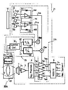
Referring now to Fig. 3 in which the present
invention is shown applied to a video camera system 20A
generally~composed of a camera body 21 on which a selected
one of a plurality of exchangeable lens devices 22 is ~;~
removably mounted. Each exchangeable lens device 22 is
shown to include a respective lens assembly 2 and a memory
23, for example, in the form of a read-only-memory (ROM) in ~ ;
which there is stQred, in advance, white balance correction ;;
data Sl for use in correcting white balance errors resulting
from spectral characteristics peculiar to the respective
lens assembly 2.
When the exchangeable lens device 22 is mounted on
.:
the video camera body 21, the white balance correction data
SI stored in the memory 23 of the e:cchangeable lens device ~ ~-
2?. is read out in synchronism with a clock signal CK
suppIied by a control circuit 24 which may be in the form of
a micro-computer included in a white balance correcting
circuit 25 provided in the camera body 21. The control
circuit 24 responds to the white balance correction data SI
.
', ~.
AS19:10mk -16-
r~.t, ~
PATENT
~"` 1 3 3 0 2 3 7 39-0100.2136
, ,
read out from the memory 23 to provide red correction data
Dl and blue correction data D2 which are applied to
digital-to-analog (D/A) converting circuits 26 and 27,
respectively.
The video camera system 20A is fuxther shown to
have, as part of its camera body 21, a white balance
adjusting circuit llA of the open-loop type that is
generally similar to the white balance adjusting circuit 11
described above with reference to Fig. 2, and has its
corresponding elements identified by the same re~erence
numerals. However, the white balance adjusting circuit llA
additionally includes adding circuits 28A and 28B interposed
in the lines through which the red compensation signal STR .
and the blue compensation signal STB, respectively, are
applied, as gain control signals, to the amplifiers 5A and
~:: :. .
5C. The adding circuits 28A and 28B further have inputs
connec ed to outputs of the D/A converting circuits 26 and
27, respectively. Thus, the adding circuit 28A is operative
to add the output of the D/A CQnverting circuit 26 to the
red compensation signal STR for providing the gain control
signal for the amplifier 5A, while the adding circuit ~8B is
operative to add the output of the D/A converting circuit 27
to the blue compensation signal STB for providing the gain
control signal for the amplifier 5C.
In the operation of the video camera system 20A
according to this invention, when one e:~changeable lens
ASl9:lOmk -17-
.
. .
1 330237 39-olo0.2~36
device 22 is removed from the camera boAy 21 and replaced by
another exchangeable lens device 22, the white balance
correction data SI stored in the white balance correction
data memory 23 of the newl~ mounted lens device 22 is read :~
from the memory 23 and passed to the white-balance
correction circuit 24 which derives therefrom the
corresponding red correction data Dl and the blue correction
data D2. Such red correction data D1 and blue correction :~
data D2 are converted in the circuits 26 and 27, `.
respectively, to corresponding analog correction signals
supplied to the adder circuits 28A and 28B, respectively.
Thus, the gain control signals for the amplifiers 5A and 5C
are represented by the red and blue compensation signals STR
and STB as modified by the analog outputs of the converting
circuits 26 and 27, respectively. Accordingly, the output
g SRo~ SGo and SBo from the amplifiers 5A 5B
and 5C have their white balance properly adjusted both with ~-~
reference to the sensing of the light from the white
scattering plate 12 by the sensors 13R, 13G and 13B of the
white balance adjusting circuit llA, and also with rererence .~ ~
to the particular spectral characteristics of the lens :
assembly included in the exchangeable lens device 22 then
mounted on the camera body 21.
In the embodiment of this invention described with
reference to Fig. 3, the white balance correction data SI
characteristic of the exchangeable lens device 22 is stored
.~ , '` '';
ASl9:lOmk -18-
PATENT
- 1 3 3 0 2 3 7 39-0100.2136
in the memory 23 which is made a part of the exchangeable
lens device 22, but it is to be understood that other
arrangements may be provided in accordance with the
invention for storing the white balance correction data
characteristic of each of the exchangeable lens devices, and
for correcting the operation of the white balance adjusting~ ~-
circuit in accordance with the stored white balance
correction data corresponding to the exchangeable lens
device then mounted on the camera body.
Thus, for example, as shown in Fig. 4, in a video
camera system 20B according to another embodiment of this
invention which is otherwise the same as the camera system
20A described with reference to Fig. 3, each of the
exchangeable lens devices 22B removeably mountable on the
camera body 21B includes merely a lens identification device
29 which is operative, upon the mounting of the respective -~
exchangeable lens device 22B on the camera body 21B, to
provide a lens identification signal ID which identifies the
respective exchangeable lens device. The signal ID is
employed for accessing corresponding white halance
correction data Dl and D2 stored in a memory 30 which
replaces the control circuit 24 in Fig. 3. Apart from the
foregoing, the video camera system 20B operates similarly to
the previously described camera system 20A so that analog
; signals corresponding to the white balance correction data
Dl and D2 are der~ved from the D/A converting circuits 26
and 27 and are added to the red compensation signal STR and
ASl9:lOmk -19-
' , . ' . ' . . ' .~.: .
,: ' ' ' - :
,~,1, .,. ': ., , . , . ~ . : . .
1 330237 PAT~NT
- 39-0100.2136
,' . .
.- .,:
~he hlue compensation signal STB (Fig. 3) for providing the
gain control signals for the amplifiers 5A and 5C. Thus,
the white balance adjustment is achieved with proper
correction for changes in the spe~tral characteristics of
the lenses 2 included in the exchangeable lens device 22B
that can be mounted on the camera body 21B.
Although Figs. 3 and 4 il:Lustrate embodiments of
the invention employing white balance adjusting circuits of
the open-loop type, it is to be appreciated that the
invention is not so limited, but can be also applied to
video camera systems having white balance adjusting circuits
~ : : .:,
of the closed-loop type.
For example, as shown in Fig. 5, the present
invention may be applied to a video camera system 20C
comprised of exchangeable lens devices 22C which are
removably and interchangeably mountable on a camera body
21C provided with a white balance adjusting circuit 7 of the
type described with reference to Fig. 1. In the video ~-~
camera system 20C of Fig. 5, each of the exchangeable lens
devices 22C is provided with a memory 23C which, as in the
case of the embodiment of this invention described with
reference to Fig. 3, stores white balance correction data
SI correspondinq to the spectral characteristics o the lens
assembly 2 included in the respective e~changeable lens
device 22C. Upon the mounting of a particular lens device
22C on the camera body 21C, the respective white balance
correction data SI is read out of the memory 23C to a
'~
, '
ASl9:lOmk -20- ~
,
.
1 3 3 0 2 3 7 39-0100.2136
control circuit 24C in the camera body 21C in response to a
clock signal CK from such control circuit 24C. Similarly to ;~
the arrangement desc.ribed with reference to Fig. 3, the
control circuit 24C provides, from the data SI,
corresponding red and blue correction data Dl and D2 applied ~;
to D/A converting circuits 26C and 27C for providing
corresponding analog signals to be added to the output color '~
signals SRo and SBo~ respectively, in adding circuits 28A
and 28B. Finally, in Fig. 5, the outputs of the adding
circuits 28A and 28s are applied to the negative inputs of
the operational amplifiers 7A and 7B of the white balance ~ .
adjusting circuit 7 of the closed-loop type.
}t will be apparent that, when any one of the : '~
exchangeable lens devices 22C is mounted on the camera body
21C, and an initial white balance adjustment is performed
with,a white lens cap disposed in covering relation to the
lens assembly 2, the red and blue compensation signals
stored in the memories Ml and M2 are determined both with, ,~,
reference to any white balance errors that may be perceived
in respect to the white light provided by the white lens cap
in use, and a.lso with reference to the particular spectral .,
characteristics of the lens assembly 2 included in the
mounted exchangeable lens device 22C, as represented by the
white balance correction data SI from the memory 23C.
Thereafter, when the camera system 20C is in normal use with ~;~
the same exchangeable-lens deviee 22C mounted on the camera
body '21C, the signals S'cR and S'cB read out-of the memories -
ASl9:lOmk -21-
,,
~ ... ..
` 1 3 3 0 2 3 7 39-0100.2136
Ml and M2 as ~ain control signals for the amplifiers 5A and :~
5C ensure the maintenance of the desired white balance
adjustment.
Referring now to Fig. 6, it will be seen that
the video camera system 20D thereshown also illustrates the
application of the present invention to a white balance -~.
adjusting circuit of the closed-loop type. However, in the
video camera system 20D, an arrangement similar to that
described with reference to Fi~. 4 is employed. More
specifically, each o~ the exchangeable le~s devices 22D ~-~
removably mountable on a camera body 21D includes a lens
identification device 29D which provides a lens
identification signal ID to a memory 30D within the camera
body 21D. The lens identification signal ID accesses the
white balance correction data Dl and D2 previously stored in
the memory 30D in correspondence to the particular spectral ::~
characteristics of the respective e~changeable lens device ~ -
2?D. Thus! once again, ln the video camera system 20n, the ; ;
red and blue compensation signals ScR and ScB stored in the
memories Ml and M2 during the initial white balance
:
adjustment, and which are thereafter read out of the
memories M1 and M2 as the gain control signals S'cp and -
S'cB, compensate for the white balance errors occurring
durinq the initial adjustment, for example, due to
variations in the whiteness of the white lens cap u~ed for
~.
AS19:10mk -22-
:` ~.",;
PATE~T
1 330237 39~0100~ 36
such initial adjustment, and also compensate for the
particular spectral characteristics of the lens device 22D
used at the time of the initial adjustment.
In describiny the vldeo camera s~stems 20B and 20D
with reference to Figs. 4 and 6, merely general reference
has been made to the lens identification devices 29 and
29D, respectively. However, such lens identification
devices can be of various types. For example, as shown on ;~
Figs. 7A and 7B, the lens identification device 29 or 29D on
each exchangeable lens device 22B or 22D may be
substantially of a mechanical nature. More specifically, as
shown on Fig. 7B, for mounting each exchangeable lens device
22B or 22D on the camera body 21B or 21D, the wall or face ^
of the exchangeahle lens device which faces the camera body
when mounted thereon is conventionally provided with a
socket 71 formed with an axially extending groove 71A which,
at its inner end, communicates with a circumferential groove
71B. Further, for mounting the exchangeable lens device 22B
or 22D on the respective camera body, the latter is provided
with a boss tnot shown) engageable in the socket 71 and ~ -
ha~ing a radially projecting pin 71A' ~shown in bro~en lines
::
on Fig. 7B) which is adapted to pass through the axial
groove 71~ into the circumferential groove 71B when the boss
is received in the socket 71. ~hereafter, the exchangeable
lens device 22R or 22D can be tùrned, for example, in the
direction of the arrow A, through approximately 180 so as ;~
-- .
' ' ' '
ASl9:lOmX -23-
.
1 7 ~77 PATENT
I J 3 0 L ~ / 39-010~.2136
t
to po5ition the projecting pin 71A' within the
circumferential groove 71B as shown on Fig. 7B and thereby
lock or retain the selected exchangeable lens device on the
camera body.
Further, as shown on Fig. 7B, the wall or face of
the exchangeable lens device which confronts the camera body
when mounted on the latter has a ser.ies of openings 72A,
73A, 74A and 75A which are spaced apart along an arcuate -~
line spaced radially from the center of rotation, that is,
the center of the socket 71. When the attachment of an
exchangeable lens device to the camera body has been
completed, conductive terminals 72B, 73B, 74B and 75B which
are similarly located on the camera body and suitably
. .
spring-biased will enter the small openings 72A, 73A, 74A
and 75A, respectivel~, as schematically represented on Fig.
7A. The terminal 75B is shown to be connected to ground,
while a selected one of the openings 72A, 73A and 74A has a
contact therein electrically connected, as at 76, to a
contact in the opening 75A. Thus, when the exchangeable
lens device shown on Fig. 7A is mounted on the camera body,
the terminals 72~, 73B, 74B and 75B enter the openings 72A,
73Aj 74A and 75A, respectively. At such time, the contact
withir. one of the openings 72A, 73A and 74A, that is, within
the opening 72A ln the specific arrangement shown on Fig.
7A, is connected to ground throu~h the conductor 76
extending to the opening 75A and engaged by the grounded
terminal 75B. Thus, the terminal 72B extending into the
,, ~,, . ~.
ASl9:lOmk -24- ~ ~
PATENT
1 330237 39-()100.2136
i
opening 72A an~ engaging th~ contact therein is also
grounded and this condition is suitably detected by a
detec~or 77 within the camera body for providing the
corresponding lens identification signal ID to the memory 30
or 30D on Fig. 4 or Fig. 6, respectively. It will be
appreciated that, by selectively connecting the conductor 76
from the contact within the opening 75A to a contact within
any one of the openings 72A, 73A and 74A, three different
exchangeable lens devices can be identified.
Figs. 8A and 8B illustrate another lens
identification device that can be associated with each of
the exchangeable lens devices 22B or 22D, and in which the
face of each exchangeable lens device which confronts the
camera body when secured thereon in the same conventional
manner as described above with reference to Fig. 7B is
further provided wi~h an arcuate plate 81 on which a -
bar-code identifying the respective lens device is
impressed or printed. During the turning of the
exchangeable lens device in the direction of the arrow A on
Fig. 8B for securing the same on the camera body in the
usual manner, a bar-code reader 82 provided on the camera
body (Fig. 8A) reads the bar-code on the plate 81 for
generating the respective lens identification signal ID.
Referring now to Fig. 9, it will be seen that
another form of lens identification device that may be
.. ..
associated with each of the exchangeable lens devices 22B or
22D in Figs. 4 and 6 includes a memory ~l, for example, in
: ~
- :
ASl9:lOmk -25-
.:: ,., ~: .
1 330237 PATENT
39-0100.~136
the form of a ROM, situated in the respective exchangeable
lens device and storing lens identification data ID, as
distinguished from white balance correction data SI, as in
the memories 23 and 23C in Figs. 3 and 5, respectively.
When the exchangeable lens device 22B or 22D is mounted on
the camera body, a control circuit 92 included in the camera
body is operative to provide the clock signal CK for reading
from the memory 91 the lens identification data or signal ID
which accesses the memory 30 or 30D in Fig. 4 or Fig. 6 to
obtain the respective stored white balance correction data
Dl and D2.
Referring now to Fig. 10, it will be seen that a
video camera svstem 20E according to an embodiment of this ;;
invention may be provided with a ully-automatic white`
balance adjusting circuit of the closed-loop type. Such
fully-automatic white balance adjusting circuit of the
closed-loop type is to be distinguished from the white
balance adjusting circuits 7 of the closed-loop type
included in the embodiments of the invention described above
with reference to Figs. 5 and 6, and in which a white lens
cap or the like has to be interposed in the field of view of
the lens assembly 2 included in the exchangeable lens device
22C or 22D during an initial adjustment of the white
balance. On the other hand, in the white balance adjustin~
circuit 7E included in the camera body 21E of the video
camera system 20E according to the embodiment of the present
'
.` ~;
AS19:10mk -26- ` ~
1-Z7n ~ 7 7 PATENT
l ~ U~ ~/ 39-0100.2136
invention shown in Fig. 10, such white lens cap or its
equivalent is not required and a sufficiently white signal
is automatically detected from the input video signal Sv
provided by the image pickup device 1 in response to the
projection of an image thereon by the lens assembly 2 of the
exchangeable lens device 22E then mounted on the camera body
21E. Such automatically detected white signal is then
employed for effecting the white balance ~orrection.
More specifically, in the video camera system 20E
according to the embodiment of the present invention shown
on Fig. 10, the output color signals SRo~ SGo and SBo from
the amplifiers 5A, 5B and 5C are supplied to averaging
circuits 108B, 108G and 108R, respectively, in which such
output color signals are averaged for a predetermined time
period, for example, for more than 6 field intervals. The
averaged outputs from the averaging circuits 108G and 108R
are supplied to the positive and inverted terminals,
respectively, of the operational amplifier 7A. Similarly,
the averaged outputs of the averaging circuits 108G and 108B
are supplied to the positive and inverted inputs of the
operational amplifier 7B. The output signals from the
operational amplifiers 7A and 7B are supplied through a
switching circuit SWl, upon closing of the latter, as the
xed ~nd blue compensation signals ScR and ScB to be stored
in the memories Ml and M2, respectively. Such red and blue
compensation signals stored in the memories Ml and M2 are
' .
ASl9:lOmk -27-
.
:' ,
PATENT
1 3 3 0 2 3 7
read from the respective memories as the gain control
signals S'cR and S' CB for the variable gain amplifiers 5A -:
and 5C so as to effect white balance adjustment. In other
words, when the switching circuit SWl is closed or turned
ON, a so-called closed-loop control operation is performed
in which the output levels of the averaging circuits 108R
and 108B are made equal to the output level of the averaging
circuit 108G. ~:
Further, in the white balance adjusting circuit 7E ~
according to the embodiment of the invention shown on Fig. :
10, the outputs of the averaging circuits 108R, 108G and :
108~ are applied to inverted inputs of comparators lO9R,
lO9G and lO9B, respectively, which have their outputs
supplied to a judging circuit 110. Reference voltage
sources lllR, lllG and 111~ supply predetermined reference
voltages ER, EG and EB, respectively, to positive inputs of
the comparators lO9R! 109G and lO9B, respectively. The
udging circuit 110 is operative to determine, from the
outputs of the comparators lO9R, lO9G and lO9B, whether the
ncident light LAl projected on the pickup element 1 is a
normal or substantially white li~ht, or an abnormal light. :-
Thus, for example, when the level of one of the red, green ;~
:~ :and blue signal components SR, SG and SB is extraordinarily
high or low in comparison with the other two color
eomponents, the ~udging circuit 110 determines, from the
corresponding outputs of the comparators lO9R, ln9G and
lO9B, that the incident light LAl is abnormal and, in
ASl9:lOmk -28-
: ~
1 3 3 0 2 3 7 3~-0100.2136
response to such determination, provides a switch control
signal Ss by which the switching circuit SW1 is turned OFF.
In other words, the previously described closed-loop control
is effected only when the incident light LA1 is determined
to be a normal or substantially white light in response to
which the judging circuit 110 provides the control signal Ss
at a level to turn ON the switching circuit SW1. On the
other hand, when the incident light LAl is determined to be
abnormal so that the switching circuit SW1 is turned OFF,
and the values of the red and blue compensation signals ScR
and ScB stored in the memories M1 and M2, respectively,
remain unchanged.
Further, in the embodiment of the invention shown
on Fi~. 10, each exchangeable lens device 22E for removable
mounting on the camera body 21E includes a memory 23E which, :
as in the embodiment of Fig. 5, stores white balance
correction data SI corresponding to the spectral
characteristics of the lens assembly 2 included in the
respective e~change~hle lens device 22E. Upon the mounting
~f a particùlar lens device 22E on the camera body 21E, the .
- :-
respective white balance correction data SI is read out of
the memory 23E to a control circuit 24E in the camera body :~
21E in response to a clock siqnal CK from such control
circuit. Similarly to the arrangement described with
re-erenGe to Fig. 5, the control circuit 24E provides, from
the data SI, corresponding red and blue correction data D1
AS19:10mk -29-
. ''
PATENT
1 330237 39-0100.2136
and D2 applied to D/A converting circuits 26E and 27E,
respectively. The control circuit 24E additionally
provides, from the data SI, green correction data D3 applied
to a D/A converting circuit 112. The D/A converting
circuits 26E, 27E and 112 provide analog signals
corresponding to the red, blue and green correction data D1,
D2 and D3, respectively, to be added, in adding circuits
113R, 113B and 113G, to the reference voltages ER, EB and EG
from the sources 111R, lllB and lllG. Thus, it will be
apparent that the reference voltages actually applied to the
comparators lO9R, lO9B and lO9G are modified somewhat by the
analog signals from the converters 26E, 27E and 112, ;~ -
respectively, that is, in accordance with the spectral
.
characteristics of the lens assembly included in the
exchangeabie lens device Z3E, for thereby effecting the
white balance correction in accordance with this invention.
Referring now to Fig. 11, it will be understood
that the video camera system 20F accoæding to the embodiment
of the invention there partially illustrated generally :~
comprises a camera body 21F on which an exchangeable lens
device 22F is removably mounted, and is generally similar to .
the video camera system 20E described above with reference
to Fig. 10. In fact, the video camera system 20F differs ~::
from the video camera system 20E only in that, similarly to
the video camera system 20B of Fig. 4, each exchangeable
lens dèvice 22P includes merely a lens identification device
~,
ASl9:lOmk -30- .
PATENT
1 3 3 0 2 3 7 3g-0100.2136
29F which is operative, upon the mounting of the respective
exchangeable lens device 22F on the camera body 21F, to
provide a lens identification signal ID which identifies the
respective exchangeable lens device. In the video camera
system 20F, the signal ID from lens identification device
29F is employed for accessing corresponding white balance
correction data Dl, D2 and D3 stored in a memory 30F which
replaces the control circuit 24E in Fig. 10. The white
balance correction data D1, D2 and D3 is supplied from the
memory 30F to the D/A converting circuits 26F, 27F and 112
to provide the corresponding analog signals supplied to the
adding circuits 113R, 113B and 113G for suitably modifying
the reference voltages ER, E~ and EG for achieving the
desired white balance adjusting correction.
It will be apparent that, in all of the above
described embodiments of the invention, since white balance
correction data ~or each of the exchangeable lens devices is
stored in a suitable memory and is used to modify the ,;~
correction signals for white balance adjustment, it is
possible to provide a video camera system that can -
accurately and reliably adjust the white balance even when
using exchangeable lens devices having different spectral
charàcteristics.
Although illustrative embodiments of the invention
have been described in detail herein with reference to the
accompanying drawings, it is to be understood that the
ASl9:lOmk -31-
.
PATENT
1 330237 39-0100.2136
invention is not limited to those precise embodiments, and
that various changes and modifications may be effected
therein by one skilled in the art without departing from the
scope or spirit of the invention as defined in the appended
claims.
, .
:::: . -.:
, ~, .
-: .' :' :
. .
~, .
- ~ ,
,
- ,.
' ~
~: :
' ",. ' ~ ,:
,,
. ' . ' ' ~ ~' ~ .
ASl9:lOmk -32- ::
,
- ~.' '.