Note: Descriptions are shown in the official language in which they were submitted.
13304~
' ; :
OSCILLATING QUARTZ ATOMIC FORCE MICROSCOPE
This invention relates generally to Atomic Force Microscopes (AFM) and more
particularly to means for measuring the forces andtor deflections occurring
during operation of the AFM. The measurement is performed by means of a
pointed tip attached to an oscillating quartz crystal.
The Atomic Force Microscope proposed by G. Binnig (EP-A-.. Appln.No. 86
110 276.2) and described by G. Binnig, C.F. Quate and Ch. Gerber, Phys. Rev.
Letters, Vol.~6, No.9, March 1986, pp.930-933, employs a sharply pointed tip
attàched to a spring-like cantilever beam to scan the profile of a surface to beinvestTgated. At the distances involved, attractive or repulsive forces occur
between the atoms at the apex of the tip and those at the surface, resulting in
tiny deflections of the cantilever beam. In Binnig's proposal, this deflection is
measured ~y means of a tunneling microscope, i.e., an electrically conductive
tunnel tip is placed within tunnel distance from the back of the cantilever
beam, and the variations of the tunneling current are used to measure the
deflection. With known characteristics of the cantilever beam, the forces
occurring between the AFM tip and the surface under investigation can be
determined.
The forces occurring between a pointed tip and a surface are usually
described as van-der-Waals forces, covalent forces, ionic forces, or repulsive
core interaction forces. The energies involved in the atomic distance approach
of a single atom ~at the apex of the tip~ to a surface are in the range of
Eo = 0,01...10eV= 10-22...10-'flJoule. The corresponding distances are in the
subnanometer range of x0 = 10...1000pm = 0,01...1 nm. The respective
forces, i.e. the first derivatives of the potential function, therefore, are in the
range of Ko = 10 pN ...10 nN . The resulting atomic 'spring constants', i.e., the
second derivatives of the potential function are in the range of
1330~2
2 SZ 9-87-007 :
C0 = 100...0,01 Nlm. These data can be deduced from surface studies and
many other sources, such as the values of elastic constants.
~ .
It is one object of the present invention to describe a force measuring device
which may be used as an atomic force microscope, but which does not employ
cantilever beams nor tunneling for detection.
., .
~ Accordingly, the present invention porposes an atomic force microscope
comprising a pointed tip provided for interaction with a surface to be
investigated and means for approaching said tip to said surface to within a
i~ ~ ~ working distance on the order of one tenth of a nanometer, and for scanning
said tip across saTd surface in a matrix fashion. This atomic force microscope
i: Ts characterized In that said tip is attached to one surface of an oscillating
body carrying, on opposite sides thereof, a pair of electrodes permitting an
, ~ electrical potential to be applied, that, in operation, and with said tip remote
from said surface, said body is excited to oscillate at its resonance frequency, ~-
and that, with said tip maintained at said working distance from said surface,
said body oscillates at a frequency deviating in a characteristic manner from -~
said resonance frequency, that said deviation is compared with a reference
signal, and that the resulting differential signal is passed through a feedback
loop to control said means for approaching the tip to said surface.
Details of one embodimen~ of the invention will be described by way of
example in the following description and with reference to the drawings in
; which~
Fig.1 represents an embodiment of the force measuring device in the
j~ form of a quartzcrystal oscillator; . ~; ;
Fig.2 is an equivalent circuit of the quartz oscillator of Fig.1; i ~ -
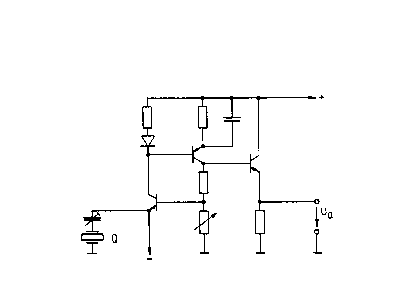
~ Fig.3 shows a circuit diagram for the quartz oscillator circuit of Fig.1;
`~ ~ - Fig.4 is a schematic diagram of the control circuitry of the quartz
oscillator.
~ ~ ,
1330~2
3 SZ 9-87-007
Refèrring to Fig.~, there is shown an atomic force measurement device
comprising a pointed tip 1 mounted on one of the vibrating surfaces of a small
Y-cut quartz crystal 2. In its 'isolated' position, quartz crystal 2 can be excited
to oscillate with its resonance frequency. When tip 1 is brought sufficiently
close to a sample surFace, the atomic forces operating between the atom at the
apex of tip 1 and one or more of the surface atoms will cause a detectable shiftin resonance frequency, as well as the generation of higher harmonics of the
excitation frequency. It can be shown that the resulting sensitivity is
comparable to that of the atomic force microscope of EP-A-.. (Appln. No.
86110Z67.2). Quartz crystal 2 is mounted on a substrate 3 which in turn is
fixed to a conventional xyz-drive 4. The hight, width and length dimensions of
quartz crystal 2 are preferably all about 0,1 mm. The crystal can be fabricated
by conventional etching and poiishing techniques (lithography). The sample to
be investigated (not shown) may be approached to tip 1 by means of a coarse
translation unit known in the art.
A voltage applied to electrodes 5 and 6 respectively coated upon two opposite
surfaces of crystal 2 will cause the crystal to perform a shear motion in
x-direction. The elastic Forces associated with this motion can be characterizedby a (static) spring constant C~,
~'! :~,'" : , !
. ~ Ce = b~h ~ 4-106 N/m,
where C66 = 4 10'N/m2 is the modulus of elasticity for the particular cut of
`~ c rystal 2, in accordance with V.E. Bottom, "Quartz Crystal Unit Design", D. Van
i~ Nostrand 1982, and w = I = h = 0,1 mm. AC excitation of crystal 2 creates ~-
; ~ an oscillatory motion of the tip normal to the sample surface; The resonances
of the Y-cut crystal (without tip/surface interaction) occur at
; (2n--1) ;
n ~: 2000[m Hz] h
;. '
~ With h = 0,1 mm, the fundamental frequency is v1 = 20 MHz.
~ :: :
13~0~2
4 SZ 9-87-007
The equivalent circuit for the quartz oscillator of Fig.1 is shown in Fig.2. Cs is
the unavoidable stray capacitance which is large compared to the capacitance
Cq associated with the quartz crystal itself. L~, and R~, are respectively the
inductance and resistance of the crystal. When incorporated in a circuit of the
l type shown in Fig.2, the osciilator is excited at its serial resonance frequency
v,:
which is determined by the properties of the quartz alone, and independent of
the stray capacitance C5.
At a distance of about 1 to 0,1 nm from the sample surface, tip 1 starts
interacting detectably with the sample. The atomic potential superimposes
upon the elastic potential of the oscillator. Said elastic potential is an even
function of the excursion Sx f tip 1 along the x-direction. The atomic potential
has no symmetry with respect to the origin of the displacement; it may be, for
: example, ar~exponentially increasing repulsion:
Eat = Eo eSx/xO
Kat = KO e
Cat = 'Co eSXIx
Herein, Eat is the atomic potential, Kat = dEat/dsx is the atomic force, Cat is the
force constant and xO is the characteristic distance of repulsion. A series
expansion ofthe atomicforce Kat yields ~
5~ + ( Z x~ ) S~ + '
Kat is small compared to the elastic force, creating a perturbation only. The ~
power series shows the following effects of the atomic force: ~ -`
~ O (x): Static Force Kol ~;
:~ ~ creates static displacement KJCe
~ which is too small for detection.
~ ~330~2
..
S~ 9-87-007
O (x'): Renormalization of spring constant
~j ~ Ce ~ Cf, + Co ~ ~
resulting in a shift of the resonance frequency.
O (x2): Source term for second harmonic
~ generation:
: ! ~ K(2) = ~ Ko ~ 5(1)2 ~
:~ ~ 2 Xo J ~ ' :
..
where (1) and (2) indicate the amplitudes at the fundamental and second
harmonic frequencies, respectively.
. ~- -
Turning now to the atomic force detection through a shift of the resonance
frequency. The quartz crystal together with the conventional circuitry of Fig. 3forms an oscillator whose resonance frequency changes owing to the atomic
interaction. The ensuing frequency shift can easily be detected with
commercially available electronic counters. Fig.4 is a schematic circuit
diagram showing the connection of crystal 2 with its driver circuitry 7, i.e. the
one shown`in Fig.3, to one input of a summing circuit 8 the other input of
which is connected to a reference ~requency generator 9. The output of
summing circuit 8 is connected to a counter 10 which is designed to deliver an
analog output signal representative of the force-induced variation of the
resonance frequency o f c~rysta 1 2 as it approaches sufface 12 to ibe
investigated. The output signal of counter 10 is also supplied to a control unit11 which controls the movements of xyz-drive 4 and, hence, of tip 1.
For a counter with assumed resolution of 2 parts in 109 and an integration time
of 1 second, using the method of "inverted counting", the resulting force
sensitivity Km~n is:
'.' ~
Kmjn = ( v--1 ) ce xO-
For xO = 0,1nm, Km,n = 210-'2 N. This is sufficient to detect even very weak
atomic interactions. The output signal of the counter can be used to control
: ~ the average tip position in accordance with the circuit diagram of Fig.2
~.- :
i3~4~2
6 SZ 9-87-007
,
The observation time t9 is 1 second for K~, = Kmjn. Above the noise level, tg islinearly proportional to 1/Ka~. Stronger interactions in the range of 100 to 1000
pN, therefore, can be detected within 1 to 10 ms.
The absolute value of the frequency shift is independent of the resonance
-1 frequency since both, v, and Ce scale with 1/h. The resulting shift ~v is:
~'
~v ~ 2000[m Hz] C0/c66 w I
= 5 [Hz/ m ], for w = I = 0,1 mm.
C0 = 0,01to100 Nlm hence provides ~v = 0,05to~00 Hz. ~ ;
~,
An alternative way of atomic force detection is by second harmonic generation.
The term O(x2) in the above expansion creates a force term K(2~ at twice the
excitatlon frequency. This force causes a secondary oscillation of quartz
crystal 2 w~hich in turn creates a second harmonic voltage signal at electrodes
: 4 and 5. The signal is proportional to the second derivative of the atomic force
versus distance. In order to make this signal large, one chooses v = v,/2,
such that the second harmonic excites the fundamental resonance of quartz
crysta! 2. The amplitude becomes s(2) = K(2) Q/Ce~ with Q being the quality
.~ factor of the quartz oscillator, typicaliy on the order of 105.' Because of this
large value, 5(2) typically is only two orders of magnitude smaller than s('). The
;~ respective induced charge is of the order of 10-~6 Coulomb, resulting in a
current of 10 nA at 10 MHz. ~ ~
The induced voltage depends on the stray capacitance. Assuming Cs = 4 Pf~ -
one arrives at U(2) = 0,1 ,~lV. The power U(2~-1(2) amounts to 10-'4W. The
respective thermal noise power for a bandwidth of 100 Hz is 10-'8W. The
second harmonic signal hence also can be detected and used for atomic force
measurements.
The Y-cut for crystal Z was chosen in this example only because it allows for
particularly simple calculations, but it is not optimal for thermal stability. AT-,
~j :
.. . .
... ~ ,.
.. ~j: . . .~ . - -
~330~2
.
7 SZ9 87-007
BT-, and SC-cuts permit oscillators with considerably smailer thermal drifts.
Mounting of those is, however, more diflicult since the crystal base in general
is not a nodal plane. Accordingly, the crystal support requires a more
sophisticated design.
:,.
The electronic counter used for the frequency shift determination should
j preferably employ an external reference oscillator mounted in juxtaposition
with crystal 2.
While Fig. 1 shows tip 1 mounted on top of crystal 2, the tip may
advantageously also be incorporated into crystal 2 so as to form an integral
part of the crystal. Those skilled in the art will appreciate that quartz crystal 2
may be sub]ected to a conventional etching operation to produce a tip
protruding from one of ttie crystal's surfaces.
For certain applications it may be advantageous to replace the quartz crystal
by other piezoelectric materials.
,;
~`';
,~
!,~
::
: ~ '
~ .
.:
~,",i
:
-.' , , '.. :