Note: Descriptions are shown in the official language in which they were submitted.
330~76
TRANSIENT VOLTAGE SUPPRESSION FOR ELECTRO-OPTIC MODULES
Field of the Invention
This invention relates to fiber optic modules for
fiber optic links used to connect various system elements in
a telephone switching system.
Background of the Invention
In a telephone switching system using fiber optic
links between various system elements, electro-optic
transmitter and receiver modules are used to terminate each
end of the optical link. Each serve as the electronic/optical
interfaces between the equipment and the fiber. Electronic
equipment must be protected from electro-static voltage
(ESD), or transient voltages which it may be exposed to, by
adjacent equipment, or craftsperson servicing the equipment.
Such destructive voltages may be in the range of a few
hundred volts to thousands of volts.
Because total protection from ESD is very
difficult, separation of the electronic ground return path
became a common practice. Any hits from ESD may then be
conducted on metallic surfaces to the frame ground, which is
in turn solidly connected to the regulatory building ground.
Although optical signals are not affected by ESD, the
electrical components can be.
Physically, the modules are located on a circuit
card which is attached to one side of the backplane. In some
instances, up to twelve modules including associated clock
recovery circuits are located on such a card. Because of the ;
small size of the card, which can be (10.5 x 3.5) inch, and
the need to locate the modules close to the faceplate to make
the optical receptacle accessible, small module size is
required. In addition, the module should be able to relieve
strain to the hybrid from forces associated with the fiber
optic connector and cable, provide general mechanical
protection, EMI shielding with grounding, heat transfer away
from electronic components, and provide minimal resistance to
the general flow of cooling air over the PCB.
.
: - " .
.. ~., . , ' ~ ~ . , - .
1330576
Although electro-optic modules of small size
already exist, these have an optical connector with a
metallic liner or shell to provide increased rigidity. Even
with the connector grounded to the equipment ground, it was
found that unwanted signals and high voltage transients were
affecting the operation of the internal components of the
module, and other electronic circuits on the circuit card.
There is accordingly a need for an improved
electro-optic module able to sustain high voltage transients,
able to eliminate unwanted signals while retaining its small
size and rigidity as well as meeting the above requirements.
Summary of the Invention
It is therefore an object of the present invention
to provide an improved electro-optic module and grounding
scheme which will provide a discharge path for high voltage -~
transients, away from the module containing the electronic
and opto-devices, while meeting the above design
requirements. -~
According to a first embodiment of the invention,
there is provided, an electro-optic module for connecting to
an optical fiber and which is comprised of an optical
connector having a connecting end adapted to receive and
secure an optical fiber cable, a circuit board attached to
the optical connector and which is electrically isolated
therefrom and means for isolating the circuit board from the
connecting end of the optical connector.
According to a second embodiment of the invention,
there is provided, an electro-optic module for connecting to
an optical fiber and which is comprised of an optical
connector having a connecting end adapted to receive and
secure an optical fiber cable, a circuit board attached to -
the optical connector and which is electrically isolated
therefrom, and a conductive outer shell disposed around the
optical connector and extending from the connecting end to a
point along the connector, which is disposed away from the
circuit board, such that the conductive outer shell provides
a discharge path for voltage transients.
3 133~576 . .
According to a third embodiment of the invention,
there is provided, an electro-optic module for connecting to
an optical fiber and which is comprised of a circuit board
having electro-optic devices thereon, an optical connector
with a first portion having an outer shell with an optical
fiber receptacle disposed centrally thereof, the portion
having means for receiving and securing the optical fiber, a
second portion for attaching to the circuit board and an .
isolator separating the first portion from the second portion
to isolate the circuit board from the first portion, such
that high voltage transients are directed away from the
circuit board.
Brief Description of the Drawings
Preferred embodiments of the invention will now be
described in conjunction with the accompanying drawings in ~ ::
which: ~:
Figures la and lb are front and side views of a
typical card showing the placement of electro-optic
connectors~
Figures 2a and 2b are front and side views of an :~
electro-optic module according to a first embodiment of the
invention; :
Figure 3 is a sectional view taken along lines 3-3
of Figure 2a;
Figure 4 is a diagrammatical representation of the
discharge path taken by high voltage transients with the
module of Figure 3;
Figure 5 is a sectional view of an electro-optic
module according to a second embodiment of the invention; and
Figure 6 is a diagrammatical representation of the
discharge path taken by high voltage transients with the
module of Figure 5.
Description of the Preferred Embodiment
Referring now to Figures la and lb, we have shown
a front and side view of a typical connecting card 10 used on
backplanes of telephone switching systems. As indicated
F ~
.: . . ~ :
133057~
above, advanced telephone switches now make use of electro-
optic modules 11 and 12 to send and receive high speed
information. For example, module 11 could be used as a
receiving module, whereas module 12 could be used as a
transmitting module. Card 10 supports various electronic
components 13 and is connected to the backplane of the switch
using multi-pin connectors 14 and 15. A face plate 16
separates the optical connectors 17 and 18 of modules 11 and
12 from the modules' enclosures 19 and 20 and from the other
electronic components 13. Optical fibers can be connected to
modules 11 and 12 using the necessary optical connectors
adapted to match connectors 17 and 18.
In Figures 2a and 2b, we have shown a front and
side view of an electro-optic module according to a first
embodiment of the invention. The module 30 is comprised of
an optical connector 31 having a first portion 32 used as a
connecting end and which is adapted to receive and secure an
optical fiber cable and an enclosure 33 containing a circuit
board with various electro-optic components. Enclosure 33 can
be a conventional housing for electronic components. It is
however, not required for the purpose of transient
suppression, but is normally used to shield the electronic
and optical devices from electromagnetic interference, or to
reduce electromagnetic radiation. The enclosure 33 is
attached to the optical connector 31, but is electrically
isolated therefrom by means of an isolator 34 separating the
first portion 32 of the connector 31 from a second portion 35
attached to the enclosure 33. A series of connecting pins 36
are used to secure and electrically connect the circuit board
and module 30 to the support card shown in Figure 1.
Figure 3 is a sectional view of the electro-optic
module of Figure 2a. As seen in Figure 3, the first portion
32 of connector 31, is isolated from the second portion 35
and enclosure 33 by means of a ring-shaped isolator 34. The
ring-shaped isolator allows light travelling through optical
channel 37 to reach electro-optic transducer 38. Light may
be focused on the transducer 38 by suitable means, such as a
GRIN (graded index) lens 39 or equivalent. The electro-optic
2~
;~
1330576
transducer 38 may contain an LED or LA~ER diode, or it may
have an optical detector. Various electro-optic components
40 are supported on circuit board 41 and attached to the
connector 31 via the second portion 35, thereby isolating the -
electro-optic components from high voltage transients, which
may affect these as well as other electronic components on
the card. However, the optical channel 37 is not affected by
transient voltages, electromagnetic interference or
radiation.
Figure 4 is a grounding scheme representation
using the electro-optic module of the present invention. In
a typical telephone switch, a plurality of cards are placed
side by side on a mounting rack to form a series of shelves.
When placed on the shelves, the cards are slid into
individual slots to become connected to the backplane.
Figures 4 and 5 are simple representations of the grounding
scheme used with the electro-optic module embodiments of
Figures 3 and 5. In the embodiment of Figure 4, reference
numeral 50 represents the removable card, having face plate
~0 51. The face plate is conventionally present in equipment
design practice. The plate 51 has a conductive surface, if
it is not made of metal. The electro-optic module has its
optical connector 52 extending therethrough. The enclosure
53 is secured to card 50 and electrically connected thereto
by means of pins 54. The frame of the telephone switch is
represented by side walls 55 and 56 which are connected to an
earth ground 59. If a high voltage transient is carried
along the metallic liner of the optic fiber, it will be
discharged via a physical conductive path 57 or 58 to the
equipment frame 55 or 56 and eventually to the earth ground
59. Isolator 60 isolates the circuit card from any harmful
effects of the transient voltages, without affecting the
operation of the electro-optic module and its components. A
power supply or logic ground 61 is provided for the circuit
board and the electro-optic components. The practice of
using an earth ground separated from a logic ground
eliminates the effects of unwanted frame ground induced
currents from affecting the supply ground and electro-optic
~,r~ .
#...~
~t
6 1330~76 ~
components.
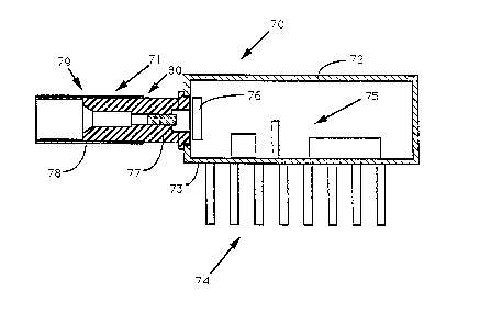
Figure 5 is a sectional view of an electro-optic ~-
module according to a second embodiment of the invention. As
seen in Figure 5, the module 70 is also comprised of an
optical connector 71 and an enclosure 72 disposed over a
circuit board 73 having connecting pins 74. Various electro-
optic components 75 are used to convert optical energy to
electrical energy, or vice-versa with transducer 76. -
However, in this embodiment, the optical connector 71 is
comprised of a single connecting element 77 made of non-
conductive material. A discharge path away from the
enclosure 72 and circuit board 73 is provided by means of a
conductive outer shell or liner 78 disposed around the
connecting element 77. The liner extends from the connecting
end 79 to a point 80 along the connector away from the
enclosure 72 and circuit board 73. Accordingly, the ;~
enclosure 72 and circuit board 73 are isolated from the ~ -
connector by the gap created between the liner 78 and the
edge of the enclosure.
Figure 6 is a grounding scheme representation
using the electro-optic module of Figure 5. Similarly, as
with the grounding scheme arrangement of Figure 4, the
physical juxtaposition of elements is the same. That is~
reference numeral 90 represents the removable card, having
face plate 91. The electro-optic module has its optical
connector 92 extending therethrough. The enclosure 93 is
secured to card 90 and electrically connected thereto by
means of pins 94. The frame of the telephone switch is
represented by side walls 95 and 96 which are connected to an
earth ground 99. However, in this embodiment, if a high
voltage transient or unwanted signal is carried along the
metallic liner of the optic fiber, it will be discharged via -
the metallic liner 100 of connector 92 through physical
conductive path 97 or 98 to the equipment frame 95 or 96 and
eventually to the earth ground 99. The gap 101 created
between liner 100 and enclosure 93 will isolate the circuit
card from any damaging effects unwanted signals might have on
the module, when carried along the fiber. A power supply or
133Q~76
logic ground 102 is provided for the circuit board and the :
electro-optic components. This practice eliminates the
effect of unwanted frame ground induced currents from
affecting the supply ground and electro-optic components. :