Note: Descriptions are shown in the official language in which they were submitted.
A RESOUR OE -DECOUPLED ARCHITECTUR~ FOR A
TE~ECOMMnNICATION~ SWITCHING SYSTEN
Field of the Invention
The invention relate~ generally to a
telecommunications switching system and more particularly to
a resource decoupled architecture ~or such a system.
Prior Art Description
In the past few decades, telephone switching
systems have evolved continuously at an accelerated rate.
The electromechanical systems such as crossbar offices gave
way to stored program centrally controlled switching systems.
These systems were then continuously enhanced as
technological progress permitted until ~inally the
contemporary fully digital switching systems were put into
service.
Throughout their evolutionary steps, all the
existing systems have maintained a similar general
architecture that usually comprises a central control unit
for processing calls and directing the operations of the
central office generally, a peripheral system for interfacing
to telephone lines and trunks, and a switching network for
interconnecting various ones of the lines and trunks. Of
course, various other subsystems, such as input-output
devices are also present.
The current generation of digital switching
systems have been optimized by building-in a substantial
amount of distributed processing. In order to maximize call
processing capacity, and at the same time to allow for
modular growth, the functions to be done by the central call
processor are held to a minimum and lower level signalling
and call processing functions are relegated as much as
possible to the peripheral subsystems.
Thus, a peripheral subsystem combines a number of
functions which appear to naturally group together; it
provides an interface function between a diverse external
world in terms of protocols and electrical interfaces and a
,., :,.,, . . :- .- .:
_ . ~, . , :
~:" .'.: ': . . ' ~ -
;'::''. ' ; :.:
~_ _J; C, ,, ", ~
unified switch internal ~orld which typically includes a TDM
(Time Division ~iultiplexing) switching network, a message
passing facility and a central processor. Thus, the
functions conventionally allocated to a current "intelligent"
peripheral unit often include A/B bit signalling (as well as
O/D bits for superframes), MF and DTMF signalling, ISDN
D-channel signalling, cellular radio control signalling, time
switching for application of tones and tone receivers and for
concentration of voice channels, digit collection and call
supervision, call progress tones as well as ringing control
and answer. The implementation of these functions as well as
others has resulted in highly complex peripheral units.
In practice, the design of a peripheral unit is a
- compromise of packaging flexibility, built-in expansion
capability, and processing capability to handle a range of
services and functions. Thus, it is much easier to optimize
a peripheral unit dedicated primarily to one type of service
than one intended for a broad range of services.
When services differ significantly in their
attributes such as PCM (Pulse Code Modulation) bandwidth
requirement, signalling methods employed and amount of call
processing necessary, a designer must choose between creating
engineerable varieties of the peripherals or under-utilizing
an over-engineered "universal" peripheral. In the first
case, a large administrative load is generated both for the
manufacturer and the user, and in the second choice, higher
product cost is incurred which has the most impact in the
lowest complexity and most frequent services such as POTS
(Plain Old Telephone Service).
A further problem arises when completely new or
unforeseen services or interfaces have to be accommodated.
If these cannot be provided by modification of the existing
design, it becomes necessary to develop new peripherals.
This has happened in the past, as for example when so-called
specialized business telephone sets were introduced in the
last few years and it is happening presently with the
introduction of ISDN (Integrated Services Digital Network)
and the DS-3 high order data rate format. In the near
~ ";,- ~ :
future, a similar problem will be encountered with the
introduction of the Sonet ~ormat and the ATM (Asynchronous
Transfer Mode) broadband services.
It is therefore an object of the invention to
provide a rasource decoupled architecture for a
telecommunications switching system.
It is a further object of the invention to provide
a telecommunications switching system architecture that
allows the flexible assignment of resources within the system
to the provision of services.
It is a still further object of this invention to
provide a switching system architecture that minimizes the
impact of new telephone network services and new data formats
on the peripheral interface subsystem of a switching system
to the telephone network.
Summary of ~he Invention
The invention provides a system architecture
~ whereby the distributed processing power of the peripheral
; 20 units is limited to that which is necessary to adapt the
formats of the external signals to the switching system
internal format in terms of timing and information channel
; arrangement. All the data information appearing at the
telephone network side of the peripheral units is reformatted
and passed into the switching system for further processing
at various levels. At a first level, the signalling
information is transduced and transmitted to a high capacity
call processor that completes the process at a second level.
It is therefore much easier to provide additional peripheral
units to accommodate new services since all intelligent or
semi-intelligent functions such as the various line and trunk
signalling schemes do not need to be re-implemented for the
new units.
Basically, the switch architecture described
herein provides a highly flexible arrangement wherein it is
possible *o provide new functions and services by increasing
the processing power of the system at its core by the
addition at the second level of one or more processors
','.'"'. ~ ' .. ,j ', ,' ' ,,
:i, . '::: . . ' ' ' ,' .,
:
suitably programmed to provide the required new functions and
services. In fact, as will become evident from the ensuing
description, the switch architecture of the invention makes
it possible to provide a telephone switching system that is a
fully intelligent node in the telephone network; that is, it
makes it practically possible to provide a switching system
capable of interfacing to almost any transmission facility to
provide POTS services for toll and/or end office functions
including custom calling services as well as function as an
integrated node for network elements such as service
switching point (SSP), signal transfer point (STP) and
service control point (SCP~.
In accordance with the invention, there is
provided an architecture for a telecommunications system
comprising a plurality of functional levels. A first level
provides a peripheral physical interface to the outside world
and functions to channelize the data appearing on the
communications facilities connected thereto. The channelized
data is passed to a digital signal processing means via a
channel switching network which effectively decouples the
peripheral interface from the processing means. The latter
functions to provide protocol conversion, channel services
and message multiplexing of the received channelized data.
At a further level, there is provided a frame switch having a
plurality of ports wherein the switch is adapted to route a
message between any two of its ports in accordance with
routing information contained in the message. The frame
; switch functions to connect the digital signal processing
means to call processing resources at a yet further level
thereby decoupling one from the other.
From another aspect, the invention provides an
architecture for a telecommunications system comprising a
first circuit means for providing physical terminations for
communication facilities and for providing channelized data
corresponding to the data on the communication facilities. A
second circuit means provides protocol conversion, channel
services and message multiplexing of the channelized data.
The first and second circuit means are connected by a channel
. ~, ,, ~
switch for passing channelized data therebetween. A third
circuit means for providing system control and call
processing resources to the telecommunications system is
connected to the second circuit means via a frame switching
means.
From yet another aspect, the invention provides a
telecommunications switching system comprising a frame switch
having a plurality of ports, the switch being adapted to
route a message between any two of its ports in accordance
with routing information contained in the message. A
plurality of application processors are each connected to a
respective port of the frame switch and at least one of the
procassors is suitably programmed to control the operation of
the switching system and another one is suitably programmed
to process telephone calls. A channel switch is connected to
receive channelized data and to switch the data between
predetermined ones of its input and output ports under
control of one of the processors. An interface circuit
connects the plurality of communication facilities from the
outside world to the switching system and is adapted to
format the information on the communication facilities into
channelized data compatible with the channel switah. A
transducer circuit connected between predetermined ports of
the channel switch and at least one port of the frame switch
formats the channelized data from the channel switch into
packetized data compatible with the frame switch and formats
the packetized data from the frame switch into channelized
data compatible with the channel switch.
; As mentioned above, the known switching system
architectures tend to be service-specific and are difficult
, , ,
to expand and modify because the services/resources are
tailored to maximum specific requirements. Once these are
reached, expansion of the capabilitiss usually entail the
redesign of the central processor and other functional units
such as the peripheral interface units.
On the other hand, the architecture of the
invention provides for the variable provisioning of the
resources at various levels independently of other levels.
r~", ,,.~, .: ~ ~ ~ ~ , . . ,- : '
'"'"''' ' '' ~ "''''"'''"'`'' ~ '~`- . ;. ......
, ~
.S . ... J
For example, the call processing resources are located at a
single level decoupled from the remainder of the system by a
frame transport system. Whenever greater call processing
resources are required, additional processors may be
connected to the frame switch whereby they are able to
communicate with the existing processing resources as well as
the remainder of the system. Similarly, the provisioning of
channel services may be modified even extensively without
affecting the peripheral equipment since they are provided by
resources decoupled from the periphery by a channel switching
network.
It should also be realized that the provision of new services
to a switching system structured in accordance with the
invention requires only that additional physical terminations
for the communication facilities be provided and that the
software of the processing resources be altered to provide
the new services. This may be achieved without modification
to the channel and frame transport systems and without re-
engineering the peripheral units.
An embodiment of the invention will now be
described in conjunction with the drawings in which:
Figure 1 is a block circuit diagram illustrating a
typical architecture of prior art telecommunications systems;
Figure 2 is a block circuit diagram of a
telecommunications system in accordance with the invention;
Figure 3 is a block circuit diagram of the channel
frame processor circuit shown in figure 2;
Figure 4 is a diagram showing the configuration
topology of the circuit shown in figure 3;
Figure 5 is a logic block diagram of the common
equipment circuit shown in figure 3;
Figure 6 is a logic block diagram illustrating the
interface interconnection between the common equipment and
the application circuits shown in figure 3;
Figure 7 is a logic block diagram of an
application circuit shown in figure 3;
Figure 8 is a block diagram of a peripheral
interface circuit shown in figure 2; and
. ~, .
~:',~,",'- , .. .......
... ) .. J
Figure 9 is a logic block diagram of a portion of
the circuit shown in figure 8.
Figure 1 illustrates an architecture for a
telecommunications switching system that is representative of
contemporary systems in existence throu~hout the world. A
full description of such a system may be found in United
States patent number 4,213,201 issued July 15, 1980, as well
as in the publications "Telesis-four" 1980 and "Telesis-
thrse" 1983, published by Bell-Northern Research Ltd. Such
systems have evolved greatly in the past few years and figure
1 represents one of the more common systems presently in use
in the North American telephone system.
Figure 1 shows a system having a duplicated
processing core 10, each half comprising a high capacity
processor with all the necessary data and program stores to
perform the functions associated with call processing.
message switch 11, also duplicated, serves to route messages
between the core 10 and a switching network 12 comprising a
pair of identical parallel planes. The data passing through
the network is switched through both planes for reliability
considerations.
In the more recent evolution of this system, the
message switch 11 is a high-speed, high-capacity frame switch
having a plurality of ports. All the components or
subsystems of the switching system are connected directly or
indirectly to the switch 11 and are thus able to communicate
with each other in a very quick and uniform manner. This
arrangement thus allows any port on a peripheral unit to have
access to the call processing core or any of applications
processors 17. New functions can be added and the capacity
of the system may be increased by connecting additional
processors to respective ports of the switch 11. The frame
switch 11 is fully duplicated and normally runs in load-
sharing mode even though each individual unit may be capable
of carrying the full messaging load on its own. The ports of
the system function in complete independence of one another,
and communication between them takes place on a port-to-port
basis over the switch 11 rather than multi-port to single
::., .::: ': ', . '
: . :
8 ~ J
port. This loose coupling between ports is made possible by
having each data packet entering a port carrying a lo~ical
address as well as a physical address. This is fully
described in United States patent number 4,816,826 issued on
March 29, 1989.
The switching network 12 is a junctorless, non-
blocking expandable switch that interconnects 64 kb/s voice
and data channels. The network 12 provides the switching
function for peripheral to peripheral traffic entering and
exiting the network via the peripheral links as well as the
messaging paths between the peripherals, the processing core
10 and the message switch 11; the latter may be provided
through semi-permanent nailed-up connections within the
matrix. The network 12 is composed of two identical planes
and reliability is achieved by a duplex arrangement where all
connections are established in both planes and peripherals
are connected to identical ports in both planes. Thus, a
true network path between any two end points is guaranteed in
a single fault situation. Each plane of the network 12 may,
for example, consist of a 128K channel matrix divided into
four units each having 32K input channels and 32K outpùt
channels. The input channels are broadcast to the other
units so that each unit has a total input capacity of 128K
- channels. Each unit can switch any of the 128K input
channels to any of the 32K output channels~ In this way, the
four units provide a total of 128K inputs by 128K outputs
non-blocking switching paths. A better understanding of this
switching network may be obtained from United States patent
No. 4,450,557.
3~ In view of their high-speed and high-capacity, the
three main elements of the system are interconnected by high-
capacity DS-512 fiber optic links. These links are capable
of carrying up to 511 ten-bit data bytes or PCM channels and
one channel for link synchronization. The link between the
channel switch 12 and the message switch 11 carries many
` time-multiplexed message channels, whereas each of the
duplicated computing modules of the processing core is
connected (not shown) to both planes of the message switch 11
~'',- .
to provide the required level of reliability.
The network 12 may be connected on the peripheral
side to the outside world via a variety of peripheral units
represented in figure 1 by a line group controller (LGC)
peripheral unit 13, a digital trunk controller (DTC~ unit 14,
and a line-trunk controller ~LTC) unit 15. These peripheral
units include interface circuits such as line concentrator
modules ~CM) and trunk modules (TM) for connection to the
lines and trunks of the telephone network. Descriptions of
this type of circuit are available from the above-identified
United States patent number 4,213,201 and various other
publications. Of course, a typical system would also include
other subsystems especially an input/output system 16 for
connection to outside facilities such as operation and
maintenance equipment.
The hardware structure of the system just
described is based on a distributed processing architecture.
Processors are located in the processing core 10, the message
switch 11, the switching network 12 as well as in each of the
LGC, DTC, LTC, LCM and TM. This structure relieves the
processing core of such routine functions as scanning,-
supervision and digit collection, all of which are real-time
intensive. The functional elements of the system communicate
via serial digital data links according to predetermined
25 formats and protocols such as DS-30, DS-30A, DS-1, DS-512 and
HDLC as well as DMS-X and DMS-Y. Descriptions of these may
be found, for example, in United States patents numbPrs
4,750,165 and 4,6g8,809, both issued to the assignee of the
present invention. Of course, DS-l (e.g. T1 carrier) is the
basic standard for digital transmission within the North
American telephone network.
As is generally well-known, the known peripheral
units that interface subscriber lines must perform such tasks
as signal processing, line supervision, line ringing and tone
generation. Speech signal processing converts analog speech
signals into digital PCM and formats it to be consistent with
that of the internal communications links of the system. In
addition, such a subsystem must be able to handle dial pulse -
and dual-tone-multifrequency (DTMF) signalling as well as
provida concentration of tha line appearances, the latter
being usually achieved through time switching techniques
within the peripheral units.
On the other hand, a trunk circuit interfaces the
switching system to the remainder of the worldwide telephone
network. Although, the DS-l (1.544 Nb/s) format is a
standard for the North American system, it exists in many
multiples such as DS-2 (6.312 Mb/s) and DS-3 ~44.736 Mb/s).
Other formats and protocols are also increasingly being used
such as the common channel signalling protocols CCIS-6 and
CCS-7 as well as HDLC and other speciali~ed data transmission
schemes including cellular radio control signalling.
Therefore, a DTC unit must be able to interface to a large
variety of external sources of data and format it to be
compatible with the switching system. This is usually
achieved by provisioning the peripheral trunk unit with a mix
of specialized trunk circuits intended to meet the expected
traffic conditions to and from the various locations.
A peripheral unit such as the LTC 15 provides an
interface to the network for a mixture of lines and trunks.
The peripheral ports to the unit are apportioned to lines and
trunks depending on the expected traffic.
In addition to the multitude of functions that
they must be able to perform, peripheral units of a switching
system are continuously being evolved to handle new
; transmission facilities and new services. For example, the
existing systems are presently being evolved to handle
integrated services digital network (ISDN) services,
integrated services node functions, and intelligent node
functions as well as being adapted to handle new data rates
such as DS-3 (43.736 Mb/s) and new optical tran~mission data -
formats such as Sonet.
The re-engineering of existing peripheral units of
a system to handle new services or a new mix of existing
services usually entails changing the software of the
processor in the peripheral units as well as the interface
hardware. This, for example, is the case with ISDN, DS-3 and
~''''~~~~' ' ~ '
~ " ~
~;,,,
~.............. .
ll
Sonet because their implementation exceeds the usual built-in
expansion capability and processing capability of existing
peripheral units.
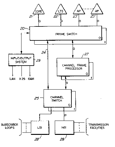
Figure 2 is a block diagram of a switching system
in accordance with the invention; it represents a radical
departure from any known system in that the peripheral units
of the system terminate only the physical layer portion of
the user/network interface. The remainder of the processing
functions are separated from the interface by the channel
switch which permits a flexible allocation of resources under
software control. The diagram shows a frame switch 20 having
a plurality of input/output ports for connection to various
units such as a call processing processor (CORE) 21, an
- application processor labelled line/trunk server (LTS) 22 and
other application processors 23. A control link 24 is also
provided to allow control signals to be transferred between
the C~RE prccessor and a channel switch 25. The switch 25
has ports connected to a high-speed interface (HSI) unit 26
as well as to a low-speed interface unit (LSI) 28; it also
has ports connected to a channel frame processor (CFP) 27
which in turn is connected to the frame switch 20.
The frame switch 20, core processor 21 and the
channel switch 25 may be the same type as the similarly
identified units described fully in conjunction with figure
1. The switch 25 is a non-blocking timeswitching network
providing constant delay and unres~ricted NX64 Kbit services
and broadband services up to the capacity of the network.
The switch 25 derives timing from the DS-512 links from the
frame switch 20. The switch control processor software may
be downloaded and the network connections controlled via
messag~s received on the control link 24.
As mentioned briefly above, the major difference
between the HSI and LSI peripherals and the prior art
peripheral units such as exemplified in figure 1, is that the
HSI and LSI peripherals terminate only the physical layer
portion of the user/network interface. User/network
signalling information, in the form of common channel
signalling as for example D-channel in ISDN PRA (primary
. ,_ .. ,.. = . ,. . . .. , . - - ~ -
~;, ~ , ; . .
~ J
12
rate) and CCS7 or associated signalling such as AB bits and
MF is passed transparently via the channel switch 25 to the
CFP 27. Procassing by various application circuits within
the CFP 27 allows access by these signalling streams to the
frame switch 20 and hence access to call processing resources
that may be resident in the call processor 21 or LTS 22 or
one o~ the application processors 23.
The HSI peripheral module is designed to support
physical termination of high speed transmission facili~ies
such as DS-l and DS-3 and may be readily adapted to support
ISDN and Sonet data. The functions of the HSI peripheral
include the physical termination of both network planes
including integrity and parity checks, the per-channel
network plane selection and the DS-0 channel formatting and
rate con~ersion between the channel switch 25 and the outside
transmission facilities. Other functions include maintenance
and alarm processing as well as slip control, clock recovery,
line driving and all other functions conventionally related
to termination of the physical layer of the facility
interface.
The channel-frame processor 27 is basically a
connection subsystem adapted to provide various channel/frame
interface functionsO As described in detail below, the CFP
may contain a flexible mix of individual application circuit
packs (ACPs) which interface channel-oriented signalling such
as AB bits and multifrequency (MF), channelized message based
signalling such as ISDN D-channels and TR-303 messaging links :-
and user data signals between the channel and frame switches.
Whereas the HSI unit channelizes the signalling information
for transmission through the channel switch 25, the CFP
recognizes the signalling and prepares frame messages for
transmission through the frame switch 20 to the appropriate
processor. The various units of the system illustrated in
figure 2 are preferably interconnected with optical fiber
links in order to take advantage of its broadband capability,
reduced electromagnetic interference (EMI) radiation and
reduced EMI susceptibility. The links may carry 10B12B
encoded data in a DS-512 format as described in United States
. . .
.,
13
patent No. 4,698,809. The fiber links are identified by a
small loop along their length.
~ n input/output system 29 has one or more ports
connected to the frame switch 20 Por communicating with the
remainder of the system including processors 21 to 23 and
other ports for connection to an operations administration
and maintenance (OAM) center as well as framed data sources
such as Ethernet and X.25 data links.
Line Trunk Server
The line~trunX sexver shown as LTS 22 in figure 2
may, in practice, be a software call processing application
running on an application processor. For all practical
- purposes it may be considered as a part of the call
processing processor 21. The combination illustrates the
capability of deloading the core processor by allocating some
functions of the core processor to another processor and have
the processors communicate via the frame switch 20. Of
course, an LTS module may also be a duplex computer module
similar to the CORE processor 21, complete with the necessary
memory elements. Similarly, new applications may be added to
the system by the addition of application processors 23.
; On existing switching systems, the major call
processing and maintenance subsystems are distributed between
the call processor and the peripheral modules and overall
coordination of these systems occurs in the central
pxocessor. In the system of figure 2 on the other hand, the
major call processing and maintenance relationships have been -~
migrated from the peripheral units to the LTS 22. Carrier
maintenance is the only system that remains in the access
peripheral and the coordination of these systems remains in
the central processor 21. The use of the LTS processor thus
allows the call processing services currently implemented on
the system of figure 1 to be used in the system of figure 2
with minimal changes; the CORE processor now communicates
with the LTS instead of the access peripheral units to
; achieve call processing. The LTS basically replaces the
functionality of the finite states machines in the prior axt
14
peripheral units, including protocol processing. The
terminal specific attributes o~ lines and trunks such as
signalling receivers, D-channel handlers, and the like are
allocated and maintained by the LTS and not the core
processor as in the prior art systems. Thus, figure 2
represents a radical departure from the existing systems in
that future or expanded services required of the switching
system will only require the addition of peripheral hardware
necessary to provide for the new format or services with
minimal impact on the existing hardware.
Channel Frame Processor
As mentioned above, the CFP provides numerous
resources/services that may be allocated to peripheral
interfaces under software control. It provides frame relay
of HDLC framed data via the message switch for applications
such as IDLC messaging, DS-1 performance reporting, D-channel
ISDN access signalling and/or user data services at rates up
to DS-l. It also provides multiplexing of peripheral
messaging links for relay to the switch core via the message
switch as well as supporting channel service circuit
applications such as tone senders/receivers, conference
bridges and the like.
These three categories of functions are
implemented by different applications hardware within the
single architectural framework of the CFP common equipment.
In this respect, the CFP is a generic subsystem which
provides an environment for the deployment of applications
specific resources and these may be digital signal processors
implemented as respective application circuits (ACP).
As shown in Figure 3, the architecture of the CFP
is partitioned into a common equipment section and an
application equipment section. The common equipment is
responsible for providing the interface between the
application equipment and the remainder of the
telecommunications switching system. It consists of a
duplicated pair of channel/frame interface (CFI) units 0 and
1 shown connected to the duplicated units of the frame switch
,,,- -.
, ;
~'.-.- -; "
. .
20 and to the duplicated units of the channel switch 25 via
fiber interface circuits (FIC) 30 and 31 and optical fiber
links. The application equipment section is shown to
comprise three duplicated ACPs: a message link multiplexer
(LMX), an HDLC frame transceiver tHFT) and a programmable
signal processor (PSP). Other ACPs such as a digital
announcement controller may of course be added to this
architecture.
The interface on the channel side is by means of a
duplex fiber link to each plane of the switching network 25
and on the frame side, to each frame switch unit.
The interface between the CFIs and the ACPs is by
means of serial links dedicated to each pair of ACPs. The
serial links are derived from the fiber links by a
multiplexing function that essentially allocates a portion of
the channel and frame side bandwidth to an ACP pair. There
are three such serial links to each pair of ACPs from each
CFI unit; one which carries the channel side traffic and two
which carry the frame side traffic destined to each frame
switch unit. The frame side serial links also carry hardware
signalling registers (not shown) that transport status
information between the CFIs and ACPs. As mentioned above,
the application equipment may consist of a plurality of ACPs
that may be deployed as duplicated pairs or as independent
units. In either case, a pair of ACPs shares the serial
links to the CFIs. It may be noted that all ACP variants are
required to offer an identical interface to the common
~quipment.
Each of the main circuit packs, CFIs and ACPs, are
independently controlled having an on-board processor (MCS)
and dedicated system message links. Messaging to all circuit
packs is accessible to the core processor of the system in
all states, (active, inactive etc.,). Note also that
messaging between the circuits is also available and may be
used to synchronize the CFP subsystem software activities.
The intercircuit messaging may utilize an external data path
via the frame switch units.
As mentioned above, the fiber interface circuits
~;' ' '' ' ' " ' ' " ' ' ' " '
16
30 and 31 are spared or duplicated as components of the fiber
links to the t~o network planes and the frame switch units.
On the other hand the CFIs may be hot-spared so that service
can be assumed by the inactive unit without loss of context
or data.
Figure 4 illustrates the "unfolded" view o~ the
architecture of the CFP and shows the topology of the channel
side separately from the frame side. The drawing essentially
indicates that two quite distinct data paths in the CFI exist
for the channel side and the frame side data path
respectively and how each duplicated pair of ACPs is
connected to the duplicated CFIs and fiber interface
circuits. For the purpose of describing data flow in the
CFP, "receive" refers to data flowing towards an ACP and
"transmit" refers to data flowing from an ACP. This
definition will be used for both the frame and channel sides.
Figure 5 is a logic block diagram of the common
equipment illustrated in figures 3 and 4 and may be used to
further explain the operation thereof. As described above,
each of fiber interface circuits 30 and 31 terminates a
~ fiber link from a network plane and converts the optical
`~ signal for interface to a quad fiber link interface circuit
(QFLIC). For the receive direction, the QFLIC extracts the
clock and frame pulse and converts the data between the
serial link rate to a parallel format which is used for
interface to the CFIs. The data and timing signals are
interfaced to each of the CFI units independently in the
transmit direction. The CFI selects the data and timing
source from the active CFI unit as indicated by a CFI
activity status circuit (ACT). The timing of the receive
data is driven by a clock and frame pulse derived from the
fiber link. In the transmit direction the timing is driven
- by the active CFI. As is conventional in the art, a switch
of activity batween the CFIs allows the switching of the
3~ common equipment from one to the other upon failure of the
active CFI.
; In the receive direction, each CFI interfaces the
serial data paths from each of the FICs to a
, ,. ., ~ . ~ , ~ , , ,
~ '", - :~ ',- -: -~,-, -- -~
rl ;~
17
receiveftransmit circuit (DTRC). At this point, the incoming
channel side data path consists of two data streams CD1 and
CD0 one from each of the FICs representing the two planes of
the network. The data from the two DTRCs is multiplexed for
interface to a host interface circuit (HIC) over a single
interface.
In the transmit direction, ten serial links are
received from the ACPs being five pairs which are logically
ORRED into five signals interfaced to the channel HIC. The
HIC converts the serial data into a parallel format and
broadcasts the same data to the two DTRCs over a single
interface. The DTRCs, one for each plane of the network,
encode the data into the fiber link code and the resulting
data is driven over parallel interfaces to the two fiber
interface circuits 30 and 31.
The channel side data path terminates at the
application hardware of an ACP as discussed below. The
serial links are interfaced to a HIC on the ACP which
converts them to parallel format. A connection memory
controls the allocation of the timeslots to the application
hardware.
' ~
Frame Side Data Path
The basic difference between the data path for the
channel side and for the frame side is that the channel side
data is plane referenced and the frame side data is load
shared. Thus, the frame side data has a separate and
dedicated data path through the common equipment for each of
the frame switch units.
The data to and from the FICs is interfaced to two
frame DTRCs one per frame switch unit. The data from the
frame DTRCs is fed to two separate frame HICs to orm a pair
of dedicated data paths each consisting of a DTRC-HIC pair.
The HICs demultiplex the fiber link timeslots into five
serial links which are exchanged with a possible five pairs
of ACPs, each link being broadcast to a pair of ACPs in the
receive path and logically ORRED from a pair in the transmit
path.
s ~
"-, ~ ~
18
As described below, the frame side data path
terminates at the application hardware of an ACP. The serial
links are interfaced to a HI~ on the ACP which converts the
data to parallel format.
The multiple serial/parallel and parallel/serial
conversions employed in the CFP allow the use of high speed
connections between various portions of the circuit which may
be physically separated due to packaging considerations.
Figure 6 illustrates the interconnection topology
between one channel interface unit and two pairs of ACPs.
Application Circui~ ~tructure
As described earlier, the channel frame processor
is interposed between the channel switch 25 and the frame
switch and acts to multiplex the channelized information into
framed information and vice-versa. At the same time, it is
provided with facilities to perform applications and services
on the data received via these two switches.
Applications/services are grouped into specialized
functions adapted to be performed by specialized application
circuits. Examples of some of these were earlier identified
in figure 3 as link multiplexer, HDLC frame transceiver, and
programmable signal processor.
- A link multiplexer (LMX) is used to relay
peripheral system messaging between the peripherals and the
system switch processing core. The LMX multiplexes a number
of peripheral messaging links interfaced on the channel side
of the CFP to a high bandwidth payload link to each of the
message switch units on the frame side of the CFP. The LMX
is provided with processing capability for the termination
and routing of messages originating at the periphery. Since
messages are duplicated over each switching network plane and
recovered transparently to the software, peripherals are
relieved of the need to recover from failure of the channel
switch. All messaging data is now assembled at the new
periph~rals and forwarded through the switching network to
the LMX for further disposition.
An HDLC frame transceiver (HFT) is used to
~ .. . .
~, . . -
J
19
terminate the HDLC framing and to relay HDLC frame data
between end user access and the frame switch of the system.
The HFT implements the framing sub layer of the layer 2
protocol for HDLC frame data interfaced on the channel side
and to the message switch on the frame side. The data passed
may be ISDN access signalling on a D-channel or may be
destined for N user data servicas. The HFT provides HDLC
frame termination and routing for ISDN B and D channels, as
well as frame relay services and IDLC remote messaging.
A programmable signal processor (PSP) provides for
flexible channel service circuit applications. These
applications may be down-loadable from the core processor.
The PSP provides a programmable signal processing resource
- for application in telephony voice or data channels. The
core of the PSP function is a plurality of digital signal
processor (DSP) cells. The DSP cells interface to both the
channel side and to the frame side links and support channel-
in/channel-out and channel-in/frame-out applications.
Figure 7 of the drawings illustrates a circuit
structure common to the ACPs so that they present a common
functional interface to the CFP common e~uipment. The ACP
structure is divided into a common hardware section and an
; application hardware section. The common hardware implements
the functionality or interface with the CFIs. A pair of
HICs 60, 61 terminates the serial links to and from each CFI
unit and provide conversion of the serial data on the links
to parallel data on a bus 62 interconnecting the aircuit
functions of the ACP. The ACP common hardware thus basically
provides the interface functions between the ACP application
hardware and the CFI hardware.
The ACP application hardware comprises application
cells realized by a processor suitably programmed to achieve
the desired functions using the data obtained from the bus
62.
Subsystem synchronization is controlled by the
~ CFIs which lock into an external timing reference and
¦ distribute the resulting clock and frame pulses to the other
circuit. These are shown connected as inputs to the ACP
I
common hardware. Basically, the external reference for the
subsystem timing is taken from the frame switch fiber links.
Activity Control
In order to ensure ruggedness of the system, each
duplicated circuit pack pair is able to determine activity
(ACT) autonomously and to switch the activity independently
over all others. This is made possible by cross-coupling
between the CFIs and each ACP pair using serial links; this
eliminates common modes of failure and interdependency in
hardware. CFI activity state is made independent of the
applications by ensuring that the CFI activity switch is
hitless to the data paths and synchronization; ACP activity
is made transparent to the CFI because the ORRING of the
shared serial links is controlled by the ACPs.
System Reset Control
The channel frame processor system is able to be
reset remotely from either of the frame switch units using
the reset system described in Canadian patent application
Serial No. 548,919 filed October 8, 1987. The reset will be
signalled to the CFP by the insertion of an alarm code
sequence into the frame side fiber link by the frame switch
unit. The insertion is accomplished under software control
by the frame switch fiber interface circuit board. Each
alarm code of a given sequence is inserted into all timeslots
on the link. Two alarm code reset sequences enable the CFIs
to be reset individually. The reset is used following
initial subsystem commissioning or if the telecommunication
switching system determines that the CFP unit is insane.
An active CFI is able to generate a reset to the
mate CFI and to each of the ACP circuits independently. The
reset of an active ACP by the CFI will initiate an ACP
activity switch.
Telephone Network Interface
As mentioned above and as shown in figure 2, the
system of the invention interfaces to the outside world via
~.. , ;. , .... - - - - -
~.. , ,~ . ~,
21
interface circuits compatible with various transmission
sources such as DS-l, DS-3, Sonet. The interface circuits
function to channelize the data from the various transmission
sources into a format compatible with that of the channel
switch 25.
Figure 8 is a block diagram of an example
interface circuit adapted to handle DS-l data. Two pairs of
trunk interface circuits (TIC) 80A, 81A and 80B, 81B are each
connected to a plurality (e.g. 28) of DS-1 transmission
sources and respond thereto to provide the conventional data
recovery functions as well as error detection, rate and
protocol conversion and clock recovery. The TICs are also
provided with a circuit for the recovery and reformatting
into a distinct stream of the signalling information (e.g.
15 A, B, C, D bits) embedded in the DS-l data streams.
The TICs, 80 and 81 generate a plurality of serial
data streams (e.g. 7) carrying 8 MHz data and these are
converted to a plurality of parallel data streams in a pair
of host processor circuits (HPC) 82A and 82B and then fed to
planes 0 and 1 of the channel switch via a pair OI FICs 83A
and 83B and fiber links 84A and 84B. As described above in
conjunction with figure 5, each FIC includes a select circuit
for selecting the data from one or the other of the HPCs as
well as formatting circuitry to generate DS-512 data and
25 interface to fiber optic links 84A and 84B.
Figure 9 is a block logic diagram of HPC 82A or
82B. It shows the connection of the serial data links from
the TICs 80 and 81 to a plurality of host interface circuits
(HIC) 90A, 91A and 92A which generate parallel data on buses
30 93A connected to DTRCs 94A which in turn generate data
compatible with the FICs 83A and 83B. Each of the HPCs 82A
and 82B also include activity circuitry 95A and 95B and a
micro-controller system (MCS) 96A and 9~B. Of course, the
activity circuits are interconnected as well as connected to
35 the select circuits of the FICs 83A and 83B.
Although the telephone network interface subsystem
of figure 8 was described using DS-l data sources as an
example, it should be clear that the system is able to
_ _ .. ........ . . . . . ........................................... .. . .
,~, ,~ ,. ; : ,: . - .
22
interface to any other facility of the telephone network
simply by replacing the TICs with circuitry adapted to
convert whatever appears on the transmission facility to data
streams compatible with the ~PCs. It should also be realized
that altering the mix of transmission facilities connected to
the system simply entail the provision of the corresponding
mix of interface cards to the telephone network since the
services/rasources of the switch are not provided at the
periphery.
It is thus seen that the invention provides a
novel architecture for a telecommunications system wherein
the peripheral access to the switch is achieved strictly at
the physical level and wherein the services and resources of
the switch are provided through the use of logical
peripherals created by processing resources within the switch
and which may be altered and/or expanded on demand.
A resource decoupled architecture such as
described herein has the flexibility to support a virtually
infinite range of services; it is able to responsively and
efficiently reconfigure generic channel and frame processing
resources to address any conceivable service which can be
supported on a wide variety of narrowband, wideband and
broadband interfaces.
, .
s~
.,., ~ . .`. ~ ,
..i ~. . . .
~i~.... ,. -. --..... , . -, :
",