Note: Descriptions are shown in the official language in which they were submitted.
j: :
:
- 1 -
DRIVING APPARA~VS 13 3181~
FIELD OF THE INVENTION AND RELATED ART
The present invention relates to a driving
apparatus, particularly a drive voltage generating
apparatus for a ferroelectric liquid crystal panel.
A conventional drive voltage generating
apparatus for multiplexing drive of a TN (twisted
nematic) liquicl crystal panel has a system, as shown in - :;., ,~
Figure 9, comprising a plurality of resistors R1 and R2
(R1 ~ R2) connected in series between voltage supplies
.
. VDD and Vss in a drive unit so as to generate voltages
~: V12~ V13~ V14~ V1s and V16 determined by voltage
division of a voltage V11 (~ VDD - VSS) according
the plurality of resistors R~ and R2. Then, a scanning
electrode driver is supplied with the voltages V11,
~ ; V12, V15 and V16, and a data electrode driver is
supplied with the voltages V11, V12, V13 and V14. The
scanning electrode driver supplies a scanning selectlon
.~.
;`-: 20 pulse with a voltage V11 and a scanning non-selection
pulse with a voltage V15 to scanning electrodes in an
odd-numbered frame operation, and a scanning selection
pulse with a voltage V12 of an opposite polarity to the
voltages V11 and V15, with respect to the voltage level
Vss as the standard, and a scanning non-selection pulse
with a voltage V16 to the scanning electrodes in an
even-numbered frame operations. On the other hand, the
~ .
~ .
... .. .. -
-.~ ' .
, .
-2- 1331813
data electrode driver supplies a data selection pulse
voltage V12 and a data non-selection pulse voltage V13
to the data electrodes ln synchronism with the scanning
selection pulse V11 in the odd frame, and a data
selection pulse voltage V11 of an opposite polarity to
the voltages V12 and V13, with respect to the voltage
level Vss, and a data non-selection pulse voltage V14
to the data electrodes in synchronism with the scanning
selection pulse voltage V12 in the even frame.
The system shown in Figure 9 further includes -
a trimmer Rv for changing the application voltage which
may be used for ad~usting a contrast of the display
panel. More specifically, by ad~usting the application
voltage trimmer Rv, the voltage levels V12 - V16 can be
varied with the voltage level V11 at the maximum so
that the voltages applied to the liquid crystal panel
can be varied. -
The scanning electrode driver and data
electrode driver are supplied with supply voltages (VDD
- Vss), and the voltage applied to a liquid crystal
pixel at the time of selection becomes V11 - V12, so
, that the maximum voltage applied to a liquid crystal
pixel depends on the withstand voltage of the drive
unit.
On the other hand, various driving methods
have been proposed for driving a ferroelectric liquid
crystal panel. In the methods described in U.S. Patent
~ . . ~ . ...... . .......... . .
~ ~ . . . .
~. ~
-3- 1331813
Nos. 4,548,476 and 4,655,561, for example, the scanning
electrode driver and data electrode driver supply
driving waveforms including voltages V11, V12, V13 and
V14 satisfying fixed ratios of V11:V12:V13:V~4 =
2:2:1:1 with respect to the scanning non-selection
signal voltage Vc whereln V11 and V12 and also V13 and ';;
V14 are respectively of mutually opposite polarities
with respect to the voltage Vc. The amplitude of the
scanning selection signal voltage is (V11 - V12), and
the amplitude of the data selection or non-selection
signal voltage is (V13 - V14), that is (V11-V~2)/2.
Now, if it is assumed that the voltage V11 is fixed as
:~ the highest voltage and division voltages V13, Vc, V14
and V12 are generated as in the above-mentioned drive
of a TN-type liquid crystal panel, and the division
voltages are used for driving a ferroelectric liquid
crystal panel, the maximum voltage applicable to a
~pixel is (Vll - V14). More specifically, if VDD - Vss
` = 22 volts, the respective voltages will be such that
V11 = 22 volts, V13 = 16.5 volts, Vc = 11 volts, V14 =
5.5 volts and V12 = O volt, and the maximum voltage
applied to a pixel will be (V11 - V14) = 16.5 volts.
In this way, if the driving of a TN-type
liguid crystal panel and that of a ferroelectric liquid
crystal panel are composed, a driving unit of the same
withstand voltage provides a smaller maximum voltage
applicable to a pixel for a ferroelectric liguid
.
' - . . ' , ~ -
. ~ :
-4- t~3~
crystal panel becau~ie of the difference between the
driving methods.
As the characteristics required of a
ferroelectric liquid crystal panel, a higher switching
speed and a wider dynamic temperature range are
required, which largely depend on applied voltages.
Figure 11 illustrates a relationship between the drive
voltage and the application time, and Figure 12
illustrates a relationship between the temperature and
10 the drive voltage. More specifically, in Figure 11, -
the abscissa represents the voltage V (voltage applied -
to a pixel shown in Figure 10), the ordinate represents ~-
- the pulse duration ~T (pulse duration shown in Figure
10 required for invertlng the orientation at a pixel),
and the dependence of the pulse duration aT on the
charge in drive voltage V is illustrated. As shown in
;~ the figure, the pulse duration can be shortened as the
drive voltage becomes higher. Next, in Figure 12, the
abscissa represents the temperature (Temp.), the
ordinate represents the drive voltage (log V) in a
logarithmic scale, and the dependence of the threshold
voltage Vth on the temperature change is shown at a
fixed pulse duration ~T. As shown in the figure, a
lower temperature requires a higher driving voltage.
It i5 underistood from Figures 11 and 12 that an
increased voltage applicable to a pixel allows for a
higher switching speed and a wider dynamic or operable
-- , _~ . ... ..... . . . .
. .: ~ - ..
. . .
- . . . , . - : , : , .
~5~ 1331813
temperature range.
On the other hand, designing of a drive unit
(IC) having an increased withstand voltage for
providing a required drive voltage results in a slow
operation speed of a logic circuit in the data
electrode driver. This is because the designing for
providing an increased withstand voltage generally
requires an enlargement in pattern width and also in
size of an actlve element in the drive unit (IC) to
results in an increased capacitance which leads to an
increased propagation delay time. Such a slow
operation speed results in a decrease in amount of
image data transferable in a fixed period (horizontal
scanning period), so that it becomes difficult to
realize a large size and highly fine liquid crystal
display with a large number of pixels as a result.
As is further understood from Figures 11 and
12, an appropriate temperature compensation must be
effected with respect to drive voltage control with a
consideration on threshold voltage, etc. In
temperature compensation with respect to a drive
voltage control, it is particularly to be noted that
mutually related drive conditions such as the pulse
duration ~T and the drive voltage are largely changed
depending on temperature, and such drive conditions
allowable at a prescribed temperature are restricted to
a narrow range. It is extremely difficult to manually
' ~ ' ,: .
. ~ .. . .. .
- - I
~ ~' -` ~: .- , .
-6- 1331813
control the pulse duration, drive voltage, etc.,
accurately in accordance with a change in temperature. -~
SUMMARY OF THE INVENTION
With the above described difficulties in view,
it ls an ob~ect of the present invention to provide a
voltage generating apparatus which allows the supply of
an effectlvely large maximum drive voltage within a
withstand voltage of a data electrode driver without a
substantial increase of the withstand voltage, and also
a driving apparatus using the same.
Another ob~ect of the present invention is to
provide a driving apparatus suitable for realization of
an appropriate temperature compensation.
According to a principal aspect of the present
` l m entlon, there is provided a driving apparatus
comprising:
:, ~
a) a driving unit including a scanning
electrode driver and a data eleotrode driver for
~ ivlng an electrode matrix formed of scanning
- electrodes and data electrodes, and
..
b) a drive voltage generating unit including a
first means for generating a fixed voltage, a second
~ means for generating a source voltage for providing
i ~ ~ 25 drive voltaqes for driving the electrode matrix, and a
~ third means for generating a first voltage equal to a
.. . .
subtraction of the fixed voltage from the source
;
< ~ ;
.-~ ~ -- . .- . . . : , .
-7- 1331813
voltage and a second voltage equal to a subtraction of
the source voltage from the flxed voltage.
According to another aspect of the present
invention, there is provided the driving apparatus
further provided with an appropriate temperature
compensation means.
These and other ob~ects, features and
advantages of the present invention will become more
apparent upon a consideration of the following
description of the preferred embodiments of the present
invention taken in con~unction with the accompanying
drawings.
BRIEF DESCRIPTION OF THE DRAWINGS
Figure 1 is a block diagram of a display
apparatus using a driving apparatus according to the
: present invention;
Figure 2 is a graph showing a relationship of
operation voltages and drive potentials in the present
:~ 20 invention;
Figure 3 is a diagram showing a relationship
among temperature, drive voltage and frequency;
Figures 4A and 4B are respectively a circuitry
of a driving apparatus c~f the present invention;
Figure 5 is a block diagram of a display
apparatuY uslng another driving apparatus according to
the present invention;
, . .; --. , .
r ~
,~ :: ~ -:
-8- 1331813 : ~
Figure 6 ls a circuit diagram of another power
supply circuit used in the present invention;
Figure 7 is a flow chart of operation sequence
for setting voltages used in the present invention;
5Figure 8 is a circuit diagram of another power
supply circuit used in the present invention;
Figure 9 is a block diagram of a display
apparatus using a conventional driving apparatus;
Figure 10 i8 a waveform diagram showing
driving waveforms for a ferroelectric liquid crystal
panel as used in the present invention;
Figure 11 is a characteristic chart showing a
relationship between the drive voltage and application
time for a ferroelectric llquid crystal panel; and
Figure 12 is a characteristic chart showing a
relationship between the temperature and drive voltage
for a~ferroelectric liquid crystal panel.
~ DESCRIPTION OF THE PREFERRED EMBODINENTS
.~ .
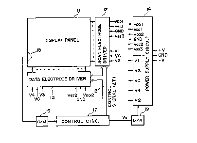
Figure 1 is a block diagram showing a driving
apparatus of the present invention. A display panel 11
includes a matrix electrode structure comprising
scanning electrodes and data electrodes intersectlng
each other. Each inter~ection of the scanning
electrodes and data electrodes constitutes together
with a ferroelectric liquid crystal disposed between
the scanning electrodes and data electrodes. The
':
.:
~9~ 1331813
orientation of the ferroelectric liquid crystal at each
pixel is modulated or controlled by the polarity of the
drive voltage applied to the pixel. The scanning
electrodes in the display panel 11 are connected to a
S scanning electrode driver 12, and the data electrode~
are connected to a data electrode driver 13.
Voltages (or potentials) VDD1, VSs1~ VDD2,
GND, VsS2 and VsS3 required for operation of the
scanning electrode driver 12 and the data electrode
driver 13, and the voltages (or potentials) V1, V3, Vc,
V4 and V2 required for operation of the display panel
11 are supplied from a power supply circuit 14 to a
driving unit including the scanning electrode driver 12
and the data electrode driver 13. Further, the power
supply circuit 14 is supplied with two external supply
voltages ~V and -V.
In the scanning electrode driver 12, the logic
circuit ic operated by a voltage of (VDD1 - Vssl), and
the output stage circuit is driven by a voltage of
(VDD1 ~ VSS3) In the data electrode driver 13, the
logic circuit is operated by a voltage of (VDD2 - GND)
and the output stage circuit is operated by a voltage
of (VDD2 - Vss2). In this embodiment, the scanning
electrode driver 12 comprises a high-voltage process IC
having a maximum rated voltage of 36 volts and
including a logic circuit showing an operation
frequency on the order of 30 kHz. Further, the data
~ . ~ . - . . .
. . . .
~-- -
.~ -
,. ~
:
tF`
~, :
. .
~- . . : .
:' '~` ' `
~, . . .
0 133181~
electrode driver 13 comprises a high-voltage process IC
having a maximum rated voltage of 18 volts and
including a logic circuit showing an operation
frequency on the order of 5 MHz. In correspondence
with this, the operational potential ranges and drive
voltage ranges are set as shown in Figure 2. The
control signal uses an input voltage range of (l5 V -
GND), and the operation voltage ranges are respectively
set as follows: scanning electrode driver logic
circuit (VDD1 ~ VSS1) = (14 V - 9 V), scanning
electrode driver output stage circuit (VDD1 - Vss3) =
(14 V - (-22 V)), data electrode driver logic circuit
(VDD2 - GND) = (5 V - O V), data electrode output stage
~: circuit (VDD2 ~ Vss2) = (5 V - (-13 V)). From the
above-mentioned drive voltage des$gn, the central
: voltage Vc among the drive voltages become Vc = -4 V,
and:the variable ranges for the respective voltages are
as follows: V1 = -4 V to ~14 V, V3 = -4 V to l5 V, V4 s
; : -4 V to -13 V, V2 = -4 V to -22 V. ~:
~: 20 A temperature sensor 15 comprising a
temperature-sensitive resistive element is disposed on .~ ,~
the display panel 11, and the measured data therefrom
are taken in a control circuit 17 through an A/D
- (analog/digital) conv rter 16. The measured
temperature data are compared with a data table
prepared in advance, and a pulse duration aT providing
an optimum drive condition based on the comparison data
" '" . ` '"`"'` ' '' ' `''`'' "' .`' ' ''', . ` ' ` ':
11 1331813
is outputted as a control signal while a data providing
a drive voltage V0 is supplied to a D/A converter 19.
The data table have been prepared in consideration of
the characteristics shown in Figures 11 and 12. An
S example of such data table reformulated in the form of
a chart is shown in Figure 3, wherein the abscissa
represents the temperature Temp. and the ordinates
represent the drive voltage V0 and frequency f ~f =
1/~T). As shown in Figure 3, if a frequency f is fixed
in a temperature range (A), the drive voltage V0
decreases as the temperature Temp. increases until it
becomes lower than Vmin. Accordingly, at a temperature
(D), a larger frequency f is fixed and a drive voltage
V0 is determined corresponding thereto. Further,
similar operation and re-setting are effected in
temperature ranges (B) and (C) and at a temperature
(E). The shapes of the curves thus depicted vary
depending on the characteristics of a particular
ferroelectric liquid crystal used, and the charts of f
and V are determined corresponding thereto.
Next, a procedure of changing a set value of
drive voltage V0 in accordance with a temperature
change is explained with reference to Figure 4A and
~igure 4C which shows an equivalent circuit of
differential amplifiers contained in Figure 4A.
A digital drive voltage V0 data from the
control circuit 17 is supplied to the ~/A converter 19
_ __. . . . ... . .. .
.: -: . : : .
~ - . -
r.~ ~
~; ' ` ' `
'` : ' ~ .:
j ~ - .
-12- 1331813
where it is converted into an analog data, which is
then outputted as a voltage Vv onto a drive voltage
control line v in a drive voltage generating clrcuit 40
in the power supply circuit 14 via a buffer amplifier
41. The drive voltage control line v is connected to
differential amplifiers D1 and D2, where differentials
between the voltage Vv and a fixed voltage Vc (= -4 V)
are taken to output a voltage V1 (= (Vv-Vc)+Vc) from
the differential amplifier D1 and a voltage V2 (= (Vc-
Vv)+Vc) from the differential amplifier D2. In thisinstance, the output voltage V1 from the differential
amplifier D1 and the output voltage V2 from the
differentlal amplifier D2 are set to have a positive
polarity and a negative polarity with respect to a
standard voltage level set between the maximum value
and minimum value of the supply voltage for driving the
~ : :: scanning electrode driver 12 and the data electrode
driver 13.
; In this embodiment, the voltage Vv on the
drive voltage control line v is set to satisfy a
:
relationship of -4 V (Vc) < Vv < ~14 V (VDD1). In this
e~bcdiment, the voltage Vv is varied in the range of -4
V to +14 V depending on temperature data. Further,
between the differential amplifiers' output V1 and V2,
four voltage division resistors R1, R2, R3 and R4 are
connected in series, and division voltages each for 1
resistor are outputted as output voltages V3, Vc and V4
:: . : . `: , ~ .
-13- 1331813
in the order of higher to lower voltages. ~hen, these
voltages are led to buffer operational amplifiers B3,
Bc and B4. In thls embodiment, in order to output
drive voltages as shown in Figure 10, the four
5 resistors R1, R2, R3 and R4 are set to have the same
resistance so as to provide ratios of voltages with
respect to the potential Vc of V1:V3:V4:V2 = 2:1:1:2.
The voltages generated by the differential amplifiers
D1, D2 and buffer operational amplifiers B3, Bc and B4
10 are supplied to current amplifiers I1, I2, I3, Ic and
I4, among the outputs from which V1, Vc and V2 are
supplied to the scannlng electrode driver, and V3, Vc
: and V4 are supplied to the data electrode driver.
According to Figure 4C showing an equivalent
: : 15 circuit of the differential amplifiers D1 and D2 in
Figure 4 in a more generalized manner, a fixed voltage
Vc provides a reference voltage for a voltage Vv which
: :
; corresponds to an input voltage to the drive voltage
generatlng clrcuit 40, and an offset voltage VOffSet
` ~ 20 provides a reference voltage for a voltage Eo which
" ~
~: corresponds to an output voltage of the drive voltage
., generating circuit 40. As a result, the following
: equations are derived.
When R11 = R12~ the pOtentials P at points
and ~ are given by:
PA ' ~Vv ~ Voffset)/2
PB = ~Vc ~ Eo~V1))/2.
, ~
',. , ., ~ : i ~. - ,. - . : ,
- -. :
- -,.
~: - - , ~: " ~ '
.~ j :, -, - - . , :
, : - ,:: .~: , .. : , :
~;. . ; . -
. . - .: .
:, , :... - . . :.. :.:. ~ - :
~ . . ..................... . .
- ~
.- :. .
s ~
~ -14- 1331813
As the differential amplifiers D1 and D2 constitute
imaginary short-circuit, PA = PB, that is,
Vv I Voffset = VC + Eo(V1)-
This leads to Vv - Vc = Eo(V1) = Voffset
S On the other hand, the potentials at points
and ~ are given by:
Pc = (-VV I Voffset)/2
PD = (-Vc ~ Eo(V2))/2.
Again PC = PD, so that
Vv ~ Voffset = Vc ~ Eo (V2),
which leads to
-VV ~ VC = EO(V2) - Voffset
Accordingly, when R11 and R12 are set to arbitrary
~; values, the following equations are given: - -
Eo(V1 ) Voffset = -(R~2/R~ ) (Vc-Vv)
` E(V2) ~ Voffset = (R12/R11)(vc-vv).
In an example set of voltages generated in the
- ; drive voltage generating circuit, the voltage Vv on the
` drive voltage control line is given as Vv = l6 V, Vc =
-4 V, VOffSet = Vc, R1~ = R~2, and then the respective
.~ drive voltages are given as follows:
Eo(V1) = -(Vc-Vv) ~ VC(=Voffset) ~6
Eo(v2) = (Vc-Vv) ~ Vc(= Voffset) 14 ~
V3 = (lV1l ~ lV2l) x 3/4 ~ V2 = ~1 V . :
~: 25 V4 = (lV1l ~ lV2l) x 1/2 ~ V2 = -9 V.
In the present invention, the offset voltage
can be set to an arbitrary value, preferably in a range
.: . - . . .
: ., ~
?.
-1s- 1331813
between the maximum output voltage and the minimum
output voltage of the circuit 40, particularly the mid
voltage in the range.
In the above embodiment, the current
amplifiers I1, I3, Ic, I4 and I2 are provided so as to
stably supply prescribed powers. In case of a TN-type
liquid crystal device in general, a capacitor i8 simply
disposed in parallel with each voltage division
resistor as the capacitive load is small. In case of a
ferroelectric liquid crystal showing a large
capacitance, a voltage drop accompanying the load
switching is not negligible. In order to solve the
problem, the current amplifiers are disposed to provide
~larger power supplying capacities, thus providing a
good regulation performance. Further, there is
actually provided a circuit structure including
feedback lines for connecting the outputs of the
current amplifiers I1 - I4 and Ic to the feed lines of
the differential amplifiers D1, D2, buffer operational
amplifiers B3, B4 and Bc, respectively, while not shown
in Figure 4, so as to remove a voltage drift of output
voltages V1 - V4 and Vc.
Figure 4B shows another embodiment of the
present invention wherein the output voltage V3 is
obtained by means of a voltage division resistor R1 and
the output voltage V4 is obtained by means of a voltage
division resistor R2.
: ;. - .::. .. .
"
: - - .. . . -
-- -. -
, ~. .. - . -- .
.
,, . . ~
- , . .
.. . .
- ,
-16- 1331813
Figure 4D shows another embodiment of the
present invention, wherein two source voltages Vv1 and
VV2 are used in combination with differential
amplifiers D1 - D5 and current amplifiers I1 - I5. In
this embodiment, the resistors are set to satisfy
R1 2/R11 = 7~ and R22/R21 3 5
Figure 5 shows another embodiment of the
present invention, wherein a drive voltage generating
circuit different from the one used in the power supply
10 circuit 14 shown in Figure 1 is used. -
In this embodiment, a power supply circuit or
unit 14 is provided with a voltage hold circuit 51, an
operational amplifier 52 and a current amplifier 53.
The voltage hold circuit 51 comprises mutually
independent four circuits for the voltages V1, V2, V
and V4, respectively. According to the circuit 51,
prescribed voltages V1, V2, V3 and V4 serially
outputted from a D/A converter 19 are sampled and held
by the respective circuits to set four voltages.
Figure 6 is a circuit diagram showing an --
example of the power supply circuit 14 according to
this embodiment. More specifically, the power supply
circuit 14 shown in Figure 6 is one provided with a
means for changing a set value of drive voltage in
25 accordance with a temperature change, and comprises
four stages including amplifiers 50a - 50b, voltage
hold circuits 51a - 51d, operational amplifiers 52a -
`
. ~ . . ~ . - . . .
~, . . . - ,. . -~
~' ' ' . :. " ',~" ~ ' ' '
-17- 1331813
52d, and current amplifiers 53a - 53d. As already
described, set voltage data Di in the form of digital
signals are sent from the above-mentioned control
circuit 17 to a D/A converter 19, where the digital
5 data are converted into analog data, which are then
supplied to the voltage hold circuits 51 a - 51 d via the
amplifier 50a for V1 /V2 and the amplifier 50b for
V3/V4- O
Figure 7 is a flow chart showing an example
10 sequence of control operation for sampling and holding
set voltages in the voltage hold circuit 51 a - 51d. In
the control sequence, first of all as shown in Figure
7, a set voltage for V1 is set in the D/A converter 19,
and a sampling signal SH1 for V1 is supplied to the
15 voltage hold circuit 51a for V1, where a set voltage v
for V1 supplied through the amplifier 50a is sampled
` and held. Then, a similar operation is repeated by
using sampling signals SH2, SH3 and SR4 to hold set
voltages v2, V3 and V4 in the voltage hold circuits
20 51b, 51c and 51d, respectively.
Then, the voltages v1, v2, V3 and V4 set in
the voltage hold circuits 51a, 51 b, 51 c and 51 d are
respectively supplied to the operational amplifiers
52a, 52b, 52c and 52d, respectively. The operational
25 ampliflers 52a - 52d are differential amplifiers
similar to D1 and D2 in Figure 4A, whereby the
differentials between the set voltages v1 - V4 and a
;~ . -. :
.,
. ,~ - . . - . . . .. : .- : ..
- -18- 1331813
fixed voltages Vc (= -4 V) are taXen. In this
embodiment, the respective set values are set to
satisfy the ranges of -4 V < v1, v2 ~ 14 V, and -4 V <
v3, V4 < 5 V. Accordingly, as a result of differential
operation by means of the operational amplifiers 52a -
52d, voltages V1 ~ V4 are generated so as to satisfy
the following conditions:
4 V ~ V1 (= (v1-vC) ~ vc) < 14 V
-22 V ~ V2 (= (VC-V2) ~ vc) < 4 V
-4 V < V3 (= (v3-vc) + vc) < 5 V
-13 V ~ V4 (= (vc-v4) ~ VC) _
- Further, the voltages generated in the
operational amplifiers 52a - 52d and a voltage follower
, ~ ~
operation amplifier 52e for Vc are respectively
; 15 supplied to the current amplifiers 53a - 53e, from
~- which the outputs V1, Vc and V2 are supplied to the
canning electrode driver 12 and the outputs V3, Vc and
V~ aro supplied to the data electrode driver 13. As
.
de~cribed above, the current amplifiers 53a - 53e are
provided 80 as to stably supply required powers.
,~, ! ~ .; ' '
In the above described embodiment, analog
voltages are retained in the voltage hold circuits.
The present invention is, of course, not restricted to
~:~
this mode, but it is possible to hold digital set
voltage~ Di as they are for providing drive voltages.
Figure 8 is a circuit diagram of a voltage hold circuit
for such an e~bcdiment. Referring to Figure 8, the
. . ,. ~ ,
~` `' ' ~; ' ' ' :
_19_ 1331813
voltage hold circuit comprises 4 sets of a data
register and a D/A converter. When sampling signals
SH1 - SH4 are supplied from the control circuit 17, set
voltage data D~ are stored in data registers 61a - 61d
5 for voltages V1 ~ V4. The data in the data registers ?~
61a - 61d are ~upplied to the D/A converters 62a - 62d
respectively connected thereto and then outputted as
the above-mentioned hold voltages v1 - V4 in analog
form.
iO As described abo~e, according to the present
invention, differentials between hold voltages v1 - v4
generated from set voltage data for providing voltages
Vl - V4 and a fixed voltage Vc are respectively taken
to provide positive voltages V1, V3 and negative
voltages V4, V2 with respect to the fixed voltage Vc as
th- reference. According to this voltage generating
system, even if a scanning electrode driver and a data
electrode driver having different rated or withstand
voltages are used, maximum drive voltages with the
^` 2D respective withstand voltage limits can be outputted as
different in a conventional voltage division by means
of resistors. Further, the above four kinds of drive
voltages can be independently varied, so that a broad
.~ .
`~ freedom is provided in drive voltage control for
temperature compen~ation. Further, it i8 not neces~ary
to use a data electrode driver having an excessively
high withstand voltage which may result in a lower
.
~ .
~~
~,. " , ~ ~ - "
1331813
operation speed.
In a preferred embodiment of the present
invention, a ferroelectric liquid crystal panel may be
used as the display panel 11. In the present
invention, it is also possible to use driving waveforms
disclosed in, e.g., U.S. Patent Nos. 4,655,561 and
4,709,995 in addition to those shown in Figure 10.
.
.':,
: