Note: Descriptions are shown in the official language in which they were submitted.
1331868
S P E C I F I C A T I O N
Title of the Invention
~ PROCESS FOR PREPARING A SUPERCONDUCTING THIN FILM
Backqround of the Invention
Field of the invention
The present invention relates to a process for preparing
a thin film of superconductor. More particularly, it relates
to a process for depositing on a substrate a superconducting
thin film of a compound oxide which is uniform in composition
and has a higher transition temperature of superconductivity.
Description of the related art
The superconductivi~y is a phenomenon which is
understood as a phenomenon of phase change under which the
electrical resistance become zero and the perfect
diamagnetism is observed. Thus, under the superconducting
condition, electric current of a very high current density
can be delivered without any loss of power.
Therefore, If the superconducting power cable is
realized, the power loss of the order of 7 ~ which is
inevitable in the conventional power cables can be reduced
greatly. Realization of superconducting coils for generating
a very high magnetic field is expected to accelerate
development in the field of fusion power generation in which
the electric power is consumed beyond its output under the
present technology, as well as in the field of MHD power
.~ . 1 ~
. . ~ .. : . - .
i- ., - ,, ~ .
t . .: . , -
` -` 13318~8
generation or motor-generators. The development of
superconductivity are demanded also in the other industrial
fields such as in the field or electric power reservation; in
the field of transportation for example magnetic levitation
trains, or magnetically propelling ships; in the medical
field such as high-energy beam radiation unit; or in the
field of science such as NMR or high-energy physics.
In addition to the abovementioned power electric
applications, the superconducting materials can be used in
the field of electronics, for example, as a device using the
Josephson effect in which guantum efficiency is observed
macroscopically when an electric current is passed through a
weak junction arranged between two superconducting bodies.
Tunnel junction type Josephson device which is a typical
application of the Josephson effect is expected to be a high-
speed and low-power consuming switching device owing to
smaller energy gap of the superconducting material. It is
also expected to utilize the Josephson device as a high
sensitive sensors or detectors for sensing very weak magnetic
field, microwave, radiant ray or the like since variation of
electromagnetic wave or magnetic field is reflected in
variation of Josephson effect and can be observed as a
quantum phenomenon precisely. Development of the
superconducting devices is also demanded in the field of
high-speed computers in which the power consumption per unit
area is reaching to the upper limit of the cooling capacity
with increment of the integration density in order to reduce
energy consumption.
.. ~
~__ . .... .. . . . .
13318~8
However, their actual usage have been restricted because
the phenomenon of superconductivity can be observed only at
very low cryogenic temperatures. Among known superconducting
materials, a group of materials having so-called A-15
structure show rather higher Tc (critical temperature of
superconductivity) than others, but even the top record of Tc
in the case of Nb3Ge which showed the highest Tc could not
exceed 23.2 K at most. This means that liquidized helium
(boiling point of 4.2 K) is only one cryogen which can
realize such very low temperature of Tc. However, helium is
not only a limited costly resource but also require a large-
scaled system for liquefaction. Therefore, there had been a
strong desire for another superconducting materials having
higher Tc. But no material which exceeded the abovementioned
Tc had been found for all studies for the past ten years.
Possibility of existence of a new type of
superconducting materials having much higher Tc was revealed
by Bednorz and Muller who discovered a new oxide type
superconductor in 1986 [Z. Phys. B64 (1986) 189]
This new oxide type superconducting material is
tLa~ Ba]2cuo4 or lLa, Sr]2cuo4 which are called as the
K2NiF4-type oxide. The K2NiF4-type oxides show such higher
Tc as 30 to 50 K which are extremely higher than the known
superconducting materials and hence it becomes possible to
use liquidized hydrogen Ib.p. = 20.4 K) or liquidized neon
(b.p. - 27.3 X) as a cryogen which bring them to exhibit the
superconductivity.
~`'; i < ' ` ' - ' :
13318~8
However, the above mentioned new type superconducting
materials which was just born have been studied and developed
only in a form of sintered bodies or as a bulk produced from
powders. The superconducting sintered bodies having a form
of a bulk inevitably contains non-reacted particles and hence
is not uniform in composition and in structure, so that they
can not be used for manufacturing electronics devices.
When the superconducting material is applied to a
variety of electronics devices, it is indispensable to
prepare a thin film of superconducting material. The
superconducting thin film, however, can not be obtained if
composition and structure of the thin film is not controlled
precisely.
It is also expected to utilize the superconducting
material to produce a superconducting elongated article
comprising a supporting member made of metal or the like in a
form of wire, stand, band, tape or the like and a
superconducting thin film vacuum-deposited on the supporting
member. In this case also, it is necessary to establish
technology how to deposit the superconducting thin film in
vacuum.
The vapour deposition technique has been used for
producing a thin film of superconducting material such as
Nb3Ge and BaPb1_xBixO3. In case of a thin film of Nb3Ge,
particles of Nb and Ge are sputtered out of several targets
each consisting of Nb and Ge respectively and are deposited
onto a substrate to form a film composed of Nb3Ge. Japanese
patent laid open No. 56-109,824 published August 31, 1981
di~closes a process for
~ 4
','' '' ~' '
.., ' ' ~. ~. "
1331868
.
producing a thin film of BaPblxBixO3 by means of sputtering
technique. But, no prior art have disclosed detailed
conditions of physical deposition of the new type compound
oxides. The present invention was completed after a variety
of experiments and examination which were done for overcome
the abovementioned problem.
Therefore, an ob~ect of the present invention is to
provide a process for producing a superconducting thin film
which is uniform in composition and structure and has the
higher critical temperature.
Su~marv of the Invention
The present invention provides a process for producing
a superconducting thin film in which the film is deposited on
a substrate by high-frequency sputtering using a target made
of a compound oside containing Ba; one element N selected from
the group consisting of Y, La, Gd, Ho, Er, and Yb; and Cu,
wherein the substrate is heated at a temperature in the range
of 450qC to 1,000C during the sputtering.
The target preferably contains perovskite type oxide or
quasi-perovskite type oxide. The term of quasi-perovskite
type oxide means a structure which can be con~idered to have
such a crystal structure that is similar to Perovskite-type
oxides and includes an orthorhombically di~torted perovskite
or a distorted oxygen-deficient perovskite or the like.
''~_
~ . .~ . . .;
~_
l ~'s: ~: :' ` . - - :-.':, '' ' ~ . - ~. '
1331868
According to one preferred embodiment of the present
invention, the target may be a preliminary sintered mass
which is obtained by sintering a power mixture of an oxide,
carbonate, nitrate or sulfate of Ba; an oxide, carbonate,
nitrate or sulfate of one element M selected from a group
consisting of Y, La, Gd, Ho Er and Yb; and an oxide,
carbonate, nitrate or sulfate of Cu, at a temperature raging
from 250 to 1,200 C, preferably 250 to 1,100 C. It is more
preferable that the target is made of a finally sintered mass
which is obtained by further sintering the abovementioned
preliminary sintere,d material or mass at a temperature raging
from 700 to 1,500 C, preferably from 700 to 1,300 C.
The term of preliminary sintering means that powder
material is subjectPd to heat-treatment or calicinated or
sintered to produce a compound oxide.
The target can be in a form of power as well as in a
form of block or mass
The target may be composed of a plurality of target
seqments, for example, three target segments consisting of
oxide of Ba, oxide of M, and oxide of Cu. Hereinafter, "M"
stands for one element selected from a group consisting of Y,
La, Gd, Ho Er and Yb. It is also possible to use two target
segments, for example, consisting of (Ba, M)OX and CuO,
wherein "x" represents a number of 1 _ x.
According to another aspect of the present invention, an
atom ratio of Cu/(Ba+M) in the tarset is selected in a range
of from 0.5 to 0.7 and an atom ratio of Ba/~Ba+M) in the
target is preferably within a range of from 0.04 to 0.97,
. ~ . , .
;. .~
:~., . - - : -- , . .
.. . . ~ -
. -. = ,
.
.
,
- 1331868
preferably from 0.1 to 0.7. The atom ratio of Ba, M and Cu
is determined on the basis of the atom ratio of Ba, M and Cu
in an objective thin film to be produced. For example, the
atom ratio can be adjusted in the function of evaporation
rates of Ba, M and Cu on the basis of the atom ratio of Ba, M
and Cu in the thin film to be produced. More precisely, the
atom ratio of Ba/(Ba+M) in the target is preferably selected
from the following ranges for respective elements M:
Atom ratio
Element "M" General range Preferable range
Ba/(Ba+Y)0.05 - 0.95 0.2 - 0.6
Ba/(Ba+La)0.04 - 0.96 0.1 - 0.4
Ba/(Ba+Gd)0.04 - 0.97 0.5 - 0.7
Ba/(Ba+Ho)0.05 - 0.96 0.5 - 0.6
; Ba/(Ba+Er)0.04 - 0.95 0.3 - 0.5
Ba/(Ba+Yb)0.05 - 0.96 0.5 - 0.6
When the abovementioned atom ratios Ba/(Ba+M) are not
higher than 0.04 and exceed 0.97, the resulting films
deposited do not exhibit desired critical temperatures of
superconductivity. The atom ratio of Ba, M and Cu in the
target is preferably determined on the basis of the atom
ratio of Ba, M and Cu in a thin film to be produced in
consideration of evaporation rates of Ba, M and Cu, because
the evaporation rates of Ba, M and Cu are not identical with
each other and because melting points of respective oxides of
.~
-` 1331868
Ba, M and Cu which are constituents of the thin film are not
identical. In other words, if the atom ratio Ba, M and Cu in
the target is not selected properly, the thin film obtained
does not have a desired composition which exhibits
superconductivity. In case of sputtering technique, the atom
ratio in the target may be determined on the basis of
sputtering coefficients of oxides of respective elements.
According to another preferred embodiment of the present
invention, a substrate on which the thin film is deposited is
preferably heated by a heater at a temperature ranging from
184 C to 1,520 C, preferably 184 C to 1,000 C during the
sputtering operation. The temperature at which the substrate
is heated is preferably selected from the following ranges
for respective systems:
Temperature of a substrate
Element "M" General range Preferable range
Y type 184 - 1,450 184 - 975
La type 285 - 1,480 285 - 980
Gd type 230 - 1,500 230 - 990
Ho type 260 - 1,500 260 - 1,000
Er type 280 - 1,520 280 - 980
Yb type ;270 - 1,480 270 - 970
The substarate may be made of one of materials selected
from a group consisting of glass, quartz, silicon, stainless
. ~ 8
,~ .~.,. . -
!~`! ' ~` `'` `: ' -~ :: ' .: ~ ` ' ` `
1331868
steel and ceramics such as MgO, BaTiO3, sapphire, YSZ or the
like.
According to another preferred embodiment of the present
invention, an atmosphere of vaporization contain Ar and 02.
The partial pressure of Ar is preferably adjusted to a range
of from 1.0 x 10~3 to 1 x 10~1 Torr, preferably 5.0 x 10~3 to
1 x 10~1 Torr, while the partial pressure of 02 is preferably
adjusted to a range of from 0.5 x 10⁻³ to 1 x 10~1 Torr,
preferably 1.0 x 10⁻³ to 1 x 1 o-1 Torr. When the partial
pressure of Ar is not higher than 1.0 x 10⁻³~ the deposition
rate become too slow to produce the thin film in industrial
scale. When the partial pressure of Ar exceeds 1 x 10~1
Torr, glow discharge occur, so that deposition of oxide which
exhibit a desired superconducting property can not be
obtained. If the partial pressure of 02 is not higher than
0.5 x 10⁻³, the resulting thin film does not contain
satisfactory amount of perovskite type oxide or quasi-
perovskite type oxide because of poor crystal structure.
When the partial pressure of 02 exceeds 1 x 10~1 Torr, the
deposition rate become too slow to produce the thin film in
industrial scale. The partial pressure of Ar and 02 are
preferably selected from the following ranges for respective
systems:
,.
. ~
. - ,..... ....-
1331868
The partial pressure of Ar (Torr)
Element "M" General range Preferable range
Y type 1.0 x 10~3 - 1 x 10~1 5 0 x 10~3 - 1 x 10~1
La type 2.0 x 10~3 - 9 x 10⁻² 6.0 x 10⁻³ - 9 x 10⁻²
Gd type 1.0 x 10~3 - 2 x 10~1 5 0 x 10~3 - 2 x 10~1
Ho type 1.0 x 10⁻³ - 3 x 10~1 5.0 x 10~3 - 3 x 10⁻¹
Er type 1.2 x 10~3 - 1 x 10~1 5 4 x 10~3 - 1 x 10~
- Yb type 1.2 x 10~3 - 1 x 10~1 5.4 x 10~3 - 1 x 10~
The partial pressure of 2 (Torr)
lOElement "M" General range Preferable range
.~
Y type 0.7 x 10~3 - 8 x 10⁻² 1.0 x 10~3 - B x 10-2
La type 1.0 x 10~3 - 9 x 10⁻² 1.1 x 10~3 - 9 x 10⁻²
Gd type 0.9 x 10~3 - 3 x 10~1 1.1 x 10~3 - 3 x 10~
Ho type 0.8 x 10~3 - 2 x 10~1 1.0 x 10~3 - 2 x 10~
Er type 0.5 x 10~3 - 1 x 10⁻¹ 1.3 x 10⁻³ - 1 x 10-
Yb type 0.6 x 10~3 - 2 x 10~1 1.1 x 10~3 - 2 x 10~
~ .
¦ According to another preferred embodiment, the physical
vapor deposition is performed by high-frequency sputtering
technique (RF sputtering). The high-frequency power is less
~han 115 W/cm~2, preferably less than 15 W/cm~2. In case of
RF sputtering, the speed or rate of deposition increase with
increase of the high-frequency power. However, if the high-
frequency power exceed 115 W/cm~2~ arc discharge or abnormal
` ~ - i 1 0
,~ ';,",'.` . '~
.,.. ,i l ~ ~
1331868
discharge is apt to occur. Therefore, the high-frequency
power which is less than 115 W/cm 2, preferably less than
15 W/cm 2 was used in the present invention.
According to further preferred embodiment, the distance
between the substrate and the target is adjusted at a value
selected from a rage of 3 to 300 mm, preferably 15 to 300 mm.
When the distance is too small, it is difficult to produce
plasma between the substrate and the target. Particularly,
in case of the high-frequency magnetron sputtering technique,
the plasma is converged or concentrated in the neighborhood
of a magnet positioned behind the target, uniform deposition
of the thin film can not be produced if the distance between
- the substrate and the target is too small. Therefore, the
distance must be larger than the predetermined minimum value.
To the contrary, when the distance between the substrate and
the target is too large, the deposition rate become too slow
to effect practical deposition. Therefore, the distance is
preferably adjusted from 3 mm to 300 mm, preferably from
15 mm to-300 mm.
The high-frequency power and the distance between the
substrate and the target can be selected from the following
ranges for respective systems:
'J'~t';' 11
l 'v'~~" ''
.. ~ . .... - - - ~
:`
``--` 1331868
The hiqh-frequencY power and
the distance between the substrate and the taraet
-
Element High-frequency Distance (mm~
"M" power ~W/cm2) General range Preferable range
Y type _ 95 4 - 230 15 - 230
La type _ 100 3 - 300 15 - 300
Gd type _ 103 3 - 225 16 - 225
Ho type _ 104 5 - 215 15 - 215
Er type _ 103 4 - 210 16 - 210
10 Yb type _ 98 4 - 221 16 - 220
According to a preferred embodiment, the thin film
obtained by the abovementioned physical vapor deposition may
be heat-treated or annealed additionally in order to reduce
the difference between the onset temperature where
superconductivity start to be observed and the critical
temperature where resistance become zero. This heat-
treatment can be carried out at a temperature ranging from
250 C to 1,700 C, preferably from 250 C to 1,200 C for
0.2 to 7 hours. Through this heat-treatment of the
substrate, the thin film is subjected to the same effect as
sintering, so that the film is changed to the proper
perovskite type oxide or quasi-perovskite type oxide.
However, if the temperature of this heat-treatment is too
high, it is difficult to control the composition of the
1331868
deposited film and hence objective the proper perovskite type
oxide or quasi-perovskite type oxide can not be obtained.
The heat-treatment permit to improve the critical
temperature (Tc) of the superconducting thin film prepared
according to the present invention and also to reduce the
difference between the onset temperature where
superconductivity start to be observed and the critical
temperature where resistance become zero. Thus, atom ratio
of oxygen in the deposited thin film can be controlled or
adjusted by this heat-treatment in order to improve the
superconducting property of the deposited film.
As described above, an object of the heat-treatment is
to homogenize the composition of the deposited thin film and
to obtain the proper perovskite type oxide or quasi-
perovskite type oxide. If the temperature of the heat-
treatment is not higher than 250 C, it is difficult to
obtain the objective perovskite type oxide or quasi-
perovskite type oxide which possess the desired critical - -
temperature of superconductivity or it takes extremely longer
time to complete the heat-treatment. To the contrary, if the
temperature of the heat-treatment exceed 1,700 C, the
objective perovskite type oxide or quasi-perovskite type
oxide is too much exhausted or disappeared, resulting in
lowering of the critical temperature. In practice, the
temperature of the heat-treatment is preferably selected in
the following ranges for respective types of "M'`: -
. ' ~.. ,,~
13
~i '
1331868
Temperature of heat-treatment (C)
-
Element "M"General rangePreferable range
Y type 270 - 1,450 270 - 1,090
La type280 - 1,480 280 - 1,100
Gd type380 - 1,700 380 - 1,200
Ho type250 - 1,650 250 - 1,150
Er type260 - 1,700 260 - 1,200
Yb type250 - 1,650 250 - 1,100
The thin film obtained according to the present
invention has the formula:
BapMqCurOx
wherein "M" represents one element selected from a group
consisting of Y, La, Gd, Ho Er and Yb and "p", "q", "r" and
"x" represent numbers which correspond to atom ratio of the
elements of Ba ,M, Cu and O.
Particularly, the thin film is considered one of the
following compound oxides or their mixture:
(Ba, M)2CuO4_x ~"x" is a number of 1 _ x)
(Ba, M~Cu03-x ("x" is a number of 1 _ x) or
(Ba, M)3Cu2O7_* ("*" is a number of 1 _ *)
The thin film obtained according to the present
invention can be also considered to have the following
compositions or their mixture: ~ -:
Y type Bao 6Yo 4CuO3 or
BaYo 3Cuo 7O3 ~ :
14
1331868
La type Bao.6Lao.4CuO3 or
BaLao.3Cuo.703
Gd type Bao.6GdO.4Cu03 or
BaGdo 3CuO.703
Ho type Hoo.6Bao.4Cu03 or
HoBao 3Cuo 703
Er type Ero.6Bao.4Cu03 or
ErBao.3Cuo.703
Yb type Ybo.6BaO.4CuO3 or
YbBao 3Cuo.703
As mentioned above, the target used in the present
invention may be a preliminary sintered mass which is
obtained by sintering a power mixture of an oxide, carbonate,
nitrate or sulfate of Ba; an oxide, carbonate, nitrate or
sulfate of one element M selected from a group consisting of
Y, La, Gd, Ho Er and Yb; and an oxide, carbonate, nitrate or
sulfate of Cu, or a finally sintered mass which is obtained
by further sintering the abovementioned preliminary sintered
material or mass. ~t is also possible to use, as the target,
a powder which is obtained by pulverizing the abovementioned
preliminary sintered mass or finally sintered mass and a
sintered block which is prepared by press-molding the
abovementioned powder.
. When the abovementioned powder of the sintered mass is
used as the target, the efficiency of evaporation can be
improved and hence higher deposition rate is achieved. The
particle size of the powder is preferably selected in a range
of from 0.02 to 3 mm, more particularly, can be selected from
} 15
,,~;
I ~
- 1331 868
the following ranges for respective systems or types of
element "M":
Particle size of sintered powder
Element "M" Particle size ~mm)
Y type 0.06 - 3
La type 0.06 - 3
Gd type 0.02 - 2
Ho type 0.03 - 2
Er type 0.03 - 2
Yb type 0.04 - 2
The target according to the present invention can be
also used in the ion plating technique in which an ion beam
from an electron gun is directed onto the target.
In fact, adjustment of components which is indispensable
to obtain the proper superconducting thin film is facilitated
because material of the target is made of sintered mass or
powder, and hence it is not scattered by sputtering gas or
the ion beam.
It is apparent from the description abovementioned that
the process according to the present invention permit to
produce a superconducting thin film made of compound oxide
having higher Tc than conventional superconducting thin film
and hence the superconducting thin film obtained according to
the present invention can be utilized advantageously in a
''
~ 16 :~ ~ `
-` 1331868
applications of thin film devices, such as Matisoo switching
elements or Josephson device, Anacker memory device or SQUID
(Superconducting Quantum Interference Device).
Now, apparatus which can be used to realize the
abovementioned process according to the present invention
will be described with reference to attached drawings which
are not limitative of the present invention.
Brief descriPtion of the drawinqs
Figure 1 illustrates an example of an sputtering machine
which can be used to carry out the process of the present
invention.
Figure 2 shows an illustrative cross section of an
embodiment of an ion plating machine which can be used in the
process according to the present invention.
An apparatus illustrated in Figure 1 shows a sputtering
machine which is used for carrying out the process according
to the present invention and includes a vacuum chamber or
bell jar 1, a material target 2 placed in the vacuum chamber
1, a high-frequency power source 3 connected to the target 2,
and a substrate 4 on which the thin film is deposited and
being faced to the target 2. A vacuum pump (not shown)
connected through a port 7 to the interior of the chamber 1
functions to create vacuum therein.
Bias voltage is impressed on the substrate 4 from a
source of high-voltage 5. The substrate 4 is heated by a
heater 6 so that the temperature of the substrate is
17
. ~.... .. ..
..-.
: `', :~ '
, . . :
. ~ - : ~..... ..
: ~ j
` - 1331868
adjustable. The bell jar l has a gas inlet 8 for introducing
argon gas.
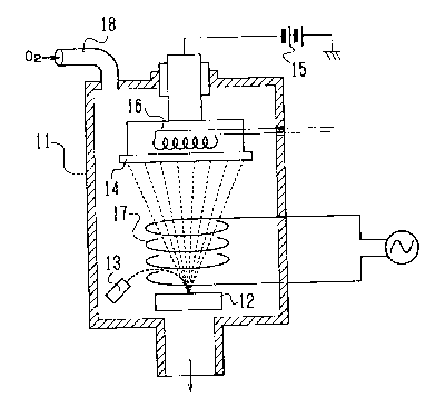
An apparatus illustrated in Figure 2 shows an ion
plating machine which can be used for carrying out the
process according to the present invention and includes a
vacuum chamber or bell jar 11, a material target 12 placed in
the vacuum chamber 11, an electron gun 13 placed in the
neighborhood of the target 12 for melting and evaporating
material of the target 12, and a substrate 14 on which the
thin film is deposited and being faced to the target 12. A
vacuum pump (not shown) connected to the interior of the
chamber 11 functions to create vacuum therein.
Bias voltage is impressed on the substrate 14 from a
source of high-voltage 15. The substrate 14 is heated by a
heater 16 so that the temperature of the substrate is
adjustable. A high-frequency coil 17 is arranged in the bell
jar 11 between the target 12 and the substrate 14 in such
; manner that evaporated particles are enclosed by the coil.
The bell jar 11 has a gas inlet 18 for introducing oxygen
gas.
Now, embodiments of the process according to the present
invention will be described with reference to illustrative
Examples, but the scope of the present invention should not
be limited thereto.
ExamPle 1 . ;;
A superconducting thin film was produced in a sputtering
machine illustrated in Fig. 1.
_. -
1331868
At first, powders of BaC03, Y2(C03)3, and CuO are mixed
uniformly in such proportions that the atom ratio of
Ba/(Ba+Y) is 0.4 and the atom ration of Ba/Cu is 2/3 and then
compacted. Then, the resulting compacted powder mixture is
subjected to a preliminary sintering at 820 C for 12 hours.
The resulting preliminary sintered mass is pulverized and
then compacted again. The resulting compacted mass is
further sintered finally at 1,080 C to obtain a target of a
sintered body. Sputtering is carried out on a substrate of
silicon crystal under the following conditions:
Partial pressure of oxygen 4 x 10⁻² Torr
Partial pressure of argon 3 x 10⁻² Torr
Temperature of the substrate 700 C
Bias voltage imposed on the substrate - 60 V
High-frequency power 25 W/cm 2
Distance between substrate and target 40 mm
A film of about 1 micron thick is obtained at a
deposition rate of 3 Angstrom/sec. For comparison, the same
operation as above is repeated but no oxygen is introduced in
~- 20 the chamber.
To determine electric resistance of the resulting thin
film, a pair of electrodes of aluminum are vacuum-deposited
on a surface of the thin film at opposite ends of the surface
and a pair of lead wires are soldered to the deposited
alumlnum electrodes.
The result was that the thin film prepared under the
partial pressure of oxygen of 4 x 10⁻² Torr according to the
present invention showed the onset temperature (from which
1 9
..
,.. - - -- .,
. .
. -
'; .
,~
. ~
-` 13318~8
superconducting phenomenon started to be appeared) of 98 K
and the critical temperature (at which the complete
superconductor is obtained) of 94 K. On the other hand, in
the comparative example in which a thin film is prepared
without introducing oxygen, although the resulting thin film
showed almost same onset temperature, the electric resistance
dropped rather qradually before it became zero at about 9 K.
This fact revealed that introduction of oxygen into the
chamber for controlling oxygen contents in the thin film
during the film formation was critical to obtain a desired
superconducting thin film.
Exam~le 2
In this Example, a powder prepared from the finally
sintered body is used as a target. Namely, the finally
sintered body obtained in Example 1 is pulverized to prepare
the powder having a average particle size of 0.3 mm and
sputtering is repeated under the same operation conditions as
Example 1 to obtain a superconducting thin film.
In this Example, higher deposition rate of
14 Angstrom/sec. than Example 1 is achieved.
The thin film prepared in this Example 2 in which a
target composed of a sintered power showed the onset
temperature (from which superconducting phenomenon started to
be appeared) of about 97 K and the critical temperature (at
which the complete superconductor is obtained) of 92 K.
This fact revealed that the efficiency of film formation
.,~ ~ 20
_ .
1331868
,
can be improved without spoiling the properties of a
superconducting thin film substantially.
Example 3
The same operation as Example 1 is repeated except that
proportions of material powders are changed and a preliminary
sintered mass is used as a target. Namely, powders of BaCO3,
Y2(CO3)3, and CuO are mixed in such proportions that the atom
ratio of Ba:Y:Cu becomes 0.9:0.25:1 and then, the mixture is
compacted and sintered preliminary at 400 C for 12 hours.
A thin film obtained by using a target of the-
abovementioned preliminary sintered mass showed the onset
~- .
temperature of about 95 ~. r.
This fact revealed that a superconducting thin film can
be produced when a preliminary sintered oxide is used as a
target.
Example 4
The thin film obtained in Example 1 is annealed at
550 C for 20 minutes under oxygen atmosphere of the partial
oxygen pressure of 0.9 x 10~1 Torr.
The superconducting transition temperatures of the
resulting annealed thin film were measured by the same method
as Example 1. The result showed that electric resistance
dropped much sharply than the case of Example 1 and the
difference between the onset temperature and the critical
temperature was 2 ~.
21
, . ~,,;
. ~, . ~ , ........ ... . .
1331868
ExamPle 5
The same operation as Example 1 is repeated except that
the final sintering temperature is changed to 920 C, the
high-frequency power is changed to 2.0 W/cm 2 and a
substarate of magnesia (MgO) is used.
The onset temperature and the critical temperature of
the resulting thin film measured by the same method as
Example 1 were 98 K and 95 K respectively.
Example 6
A superconducting thin film was produced in a sputtering
machine illustrated in Fig; 1.
At first, powders of BaCO3, La2(CO3)3, and CuO are mixed
uniformly in such proportions that the atom ratio of
Ba/(Ba~La) is 0.2 and the atom ration of Ba/Cu is 2/3 and
then compacted. Then, the resulting compacted powder mixture
is subjected to a preliminary sintering at 810 C for 12
hours . The resulting preliminary sintered mass is pulverized
and then compacted again. The resulting compacted mass is
further sintered finally at 1,070 C to obtain a target of a
sintered body. Sputtering is carried out on a substrate of
silicon crystal under the following conditions:
Partial pressure of oxygen 1 x 1o-2 Torr
Partial pressure of argon 1 x 10⁻² Torr
Temperature of the substrate 690 C
Bias voltage imposed on the substrate - 150 V
High-freguency power 20 W/cm 2
Distance between substrate and target 50 mm
-` 133~8~8
A film of about 1 micron thick is obtained at a
deposition rate of S Angstrom/sec. For comparison, the same
operation as above is repeated but no oxygen is introduced in
the chamber.
To determine electric resistance of the resulting thin
film, a pair of electrodes of aluminum are vacuum-deposited
on a surface of the thin film at opposite ends of the surface
and a pair of lead wires are soldered to the deposited
aluminum electrodes.
The result was that the thin film prepared under the
partial pressure of oxygen of 1 x 10⁻² Torr according to the
present invention showed the onset temperature (from which
superconducting phenomenon started to be appeared) of about
60 X and the critical temperature ~at which the complete
superconductor is obtained~ of 51 K. On the other hand, in
the comparative example in which a thin film is prepared
without introducing oxygen, although the resulting thin film
showed almost same onset temperature, the electric resistance
dropped rather gradually before it became zero at about 4 K.
This fact revealed that introduction of oxygen into the
chamber for controlling oxygen contents in the thin film
` during the film formation was critical to obtain a desired
superconducting thin film.
Exam~le 7
In this Example, a powder prepared from the finally
sintered body is used as a target. Namely, the finally
sintered body obtained in Example 6 is pulverized to prepare
23
. ., ~ ~.
.~...,.. t'.
- 1331868
the powder having a average particle size of 0.2 mm and
sputtering is repeated under the same operation conditions as
Example 1 to obtain a superconducting thin film.
In this Example, higher deposition rate of 9
Angstrom/sec. than Example 6 is achieved.
The thin film prepared in this Example 7 in which a
target composed of a sintered power showed the onset
temperature (from which superconducting phenomenon started to
be appeared~ of about 55 K and the critical temperature ~at
which the complete superconductor is obtained) of 49 X.
This fact revealed that the efficiency of film formation
can be improved without spoiling the properties of a
superconducting thin film substantially.
ExamPle 8
The same operation as Example 6 is repeated except that
proportions of material powders are changed and a preliminary
sintered mass is used as a target. Namely, powders of BaCO3,
La2(CO3)3, and CuO are mixed in such proportions that the
` 20 atom ratio of Ba:La:Cu becomes 0.7:0.85:1 and then, the
mixture is compacted and sintered preliminary at 400 C for
12 hours.
A thin film obtained by using a target of the
abovementioned preliminary sintered mass showed the onset
temperature of about 58 K.
This fact revealed that a superconducting thin film can
be produced when a preliminary sintered oxide is used as a
; target.
,
~-i 24
~ j t"-"'
1331868
Example 9
The thin film obtained in Example 6 is annealed at
610 C for 20 minutes under oxygen atmosphere of the partial
oxygen pressure of 1.3 x 10~1 Torr.
The superconducting transition temperatures of the .,
resulting annealed thin film were measured by the same method
as Example 6. The result showed that electric resistance
dropped much sharply than the case of Example 6 and the
difference between the onset temperature and the critical
temperature was 1 K.
Example 10
The same operation as Example 6 is repeated except that
the final sintering temperature is changed to 930 C, the
high-frequency power is changed to 1.8 W/cm 2 and a
substarate of magnesia ~MgO) is used.
The onset temperature and the critical temperature of
the resulting thin film measured by the same method as
Example 1 were 62 K and 53 K respectively.
ExamDle 1 1
A superconducting thin film was produced in a sputtering
machine illustrated in Fig. 1.
At first, powders of BaC03, Ho2(C03)3, and CuO are mixed
uniformly in such proportions that the atom ratio of
Ba/~Ba+Ho) is 0.55 and the atom ration of Ba/Cu is 2/3 and
then compacted. Then, the resulting compacted powder mixture
is subjected to a preliminary sintering at 830 C for 12
; . ... . .
i _ ....
~_ .. . . ,, , , ,, . ~
~--~ ;..:, --~
.'~
1331868
hours . The resulting preliminary sintered mass is pulverized
and then compacted again. The resulting compacted mass is
further sintered finally at 1,000 C to obtain a target of a
sintered body. Sputtering is carried out on a substrate of
I silicon crystal under the following conditions:
! Partial pressure of oxygen 1 x 10⁻² Torr
Partial pressure of argon 2 x 10⁻² Torr
Temperature of the substrate 890 C
Bias voltage imposed on the substrate - 35 V
High-frequency power 8 W/cm 2
Distance between substrate and target 20 mm
A film of about l micron thick is obtained at a ~1
deposition rate of 2 Angstrom/sec. For comparison, the same
operation as above is repeated but no oxygen is introduced in
the chamber.
To determine electric resistance of the resulting thin
film, a pair of electrodes of aluminum are vacuum-deposited
on a surface of the thin film at opposite ends of the surface
and a pair of lead wires are soldered to the deposited
aluminum electrodes.
The result was that the thin film prepared under the
partial pressure of oxygen of l x 10-2 Torr according to the
present invention showed the onset temperature (from which
superconducting phenomenon started to be appeared) of 106 K
and the critical temperature ~at which the complete
superconductor is obtained) of 100 K. On the other hand, in
the comparative example in which a thin film is prepared
without introducing oxygen, although the resulting thin film
26
,,
- 1331~6~
showed almost same onset temperature, the electric resistance
dropped rather gradually before it became zero at about 8 K.
This fact revealed that introduction of oxygen into the
chamber for controlling oxygen contents in the thin film
during the film formation was critical to obtain a desired
superconducting thin film.
Exam~le 12
In this Example, a powder prepared from the finally
sintered body is used as a target. Namely, the finally
sintered body obtained in Example 11 is pulverized to prepare
the powder having a average particle size of 0.2 mm and
sputtering is repeated under the same operation conditions as
Example 11 to obtain a superconducting thin film.
In this Example, higher deposition rate of
4 Angstromlsec. than Example 11 is achieved.
The thin film prepared in this Example 12 in which a
target composed of a sintered power showed the onset
temperature ~from which superconducting phenomenon s.arted to
be appeared) of about 105 K and the critical temperature (at
which the complete supercondùctor is obtained) of 98 K.
This fact revealed that the efficiency of film formation
can be improved without spoiling the properties of a
superconducting thin film substantially.
i~ ExamPle 13
The same operation as Example 11 is repeated except that
proportions of material powders are changed and a preliminary
27
I'' '```~ "
. , - . ,
, , : . . , ,.. :, : , ~ ., ~ . -. -
; - . . -
1331868
sintered mass is used as a target. Namely, powders of BaCO3,
Ho2(CO3)3, and CuO are mixed in such proportions that the
atom ratio of Ba:Ho:Cu becomes 0.9:0.85:1 and then, the
mixture is compacted and sintered preliminary at 400 C for
12 hours.
A thin film obtained by using a target of the
abovementioned preliminary sintered mass showed the onset
temperature of about 103 K.
This fact revealed that a superconducting thin film can
be produced when a preliminary sintered oxide is used as a
target. ~ ~-
Example 14
The thin film obtained in Example 11 is annealed at
780 DC for 20 minutes under oxygen atmosphere of the partial
oxygen pressure of 1.1 x 1 o-1 Torr.
The superconducting transition temperatures of the
resulting annealed thin film were measured by the same method
as Example 11. The result showad that electric resistance
dropped much sharply than the case of Example 1 and the
difference between the onset temperature and the critical
temperature was 3 R.
Example 15
The same operation as Example 11 is repeated except that
the final sintering temperature is changed to 940 DC~ the
high-frequency power is changed to 3.3 W/cm 2 and a
substarate of magnesia ~MgO) is used.
. , ~, ,
;~ , . .
1331868
The onset temperature and the critical temperature of
the resulting thin film measured by the same method as
Example 1 were 107 K and 102 K respectively.
Example 16 to 18
The same operation as Example 1 is repeated except that
Y2(C03)3 in the material powder is changed to Gd2(C03)3
(Example 16), Er2~C03)3 (Example 17), and Yb2(C03)3 (Example
18) respectively and that the conditions of sputtering
operation are changed or modified to the values shown in
Table 1.
The onset temperature (Tci) (from which superconducting
phenomenon started to be appeared) and the critical
temperature (Tcf) (at which the complete superconductor is
obtained) of the resulting thin film measured by the same
method as Example 1 are also summarized in Table 1.
`;t ~' ~
.," .,
1331868
Table 1
Example
16 17 18
Element "M" Gd Er Yb :~
Atom ratio :
Ba/(Ba+M) 0.6 0.4 0.55
Atom ratio
Ba/Cu 2/3 2/3 2/3
Preliminary sintering
Temperature (C) 810 840 850
Duration of Preliminary
sintering (hr) 12 12 12
Final sintering
Temperature (C) 1,000 1,040 1,050
Substrate Si Si Si
Partial pressure
of oxygen (10-2 Torr)
Partial pressure
of argon (10-2 Torr) 1 3 3
Temperature of
the substrate (C) 880 910 890
Bias voltage imposed
on the substrate (V) -90 -50 -70
High-frequency power
(W/cm~2) 5 12 30
Distance between substrate -~
and target (mm) 70 50 40 --
Deposition rate
(Angstrom/sec.) 4 3 3 - ~ -
Film thickness (micron)
Onset temperature (Tci) (K) 108 9B 95
Critical temp. (Tcf) (K) 101 92 85
. 30
,, ~ ',.
~.~....
:- . . :,, ,' :`: :,:, , ,' ' ',', ' ':: ' ' ' : '' ' ''
1331868
ExamPle 19 to 21
In these Examples 19 to 21, powders prepared from the
finally sintered body are used as respective target. Namely,
the finally sintered bodies obtained in Example 16 to 18 are
pulverized to prepare powders having average particle sizes
shown in Table 2 and sputtering operations are repeated under
the same operation conditions as Example 16 to 18 except
deposition rates are improved as are shown in Table 2.
The onset temperature (Tc) and the critical temperature
(Tcf) at which the complete superconductor is obtained of the
resulting thin films measured by the same method as Example 1
are also summarized in Table 2.
Table 2
Example
19 20 21
_
Element "M" Gd Er Yb
Average particle size
(mm) 0.2 0.3 0.3
20 Deposition rate
(Angstrom/sec.)9 5 10
Onset temperature (Tci) (K) 106 96 94
Critical temp. (Tcf) (K) 99 91 85
Example 22 to 24
The same operations as Example 16 to 18 are repeated
respectively except that proportions of material powders are
changed and targets are changed to preliminary sintered
'J_,, '.'
.~ .. . . . . . .. ... .~ .. .. .. .
. . . . - .
.~ .. . . ..
. ~ - . . . . . . . . .. .
.
. -
7. 1331868
masses. Namely, powders of BaCO3; Gd2(CO3)3, Er2(CO3)3 or
Yb2(C03)3; and CuO are mixed in such proportions that the
atom ratio of 8a : [Gd, Er or Yb~ : Cu becomes respective
values shown in the Table 3 and then, the resulting each
mixture is compacted and sintered preliminary at 400 C for
12 hours.
The onset temperature (Tci) of the resulting thin films
measured by the same method as Example 1 are also summarized
in Table 3.
Table 3
-
Example
22 23 24
Element " M " Gd Er Yb
Composition of target
(atom ratio)
Ba 0.7 0.9 0.85
Gd 0.85
Er 0.85
Yb 0-75
20 Cu 1.0 1.0 1.0
Onset temperature (Tci) (X) 105 95 92
Example 25 to 27
Each of the thin films obtained in Example 16 to 18 is
annealed at a temperature shown in Table i for 20 minutes
32
, ,~
1331868
under an oxygen atmosphere of the partial oxygen pressure
shown in the Table 4.
The superconducting transition temperatures of the
resulting annealed thin films were measured by the same
method as Example 16. The result showed that electric
resistance dropped much sharply than the case of Example 16
to 18 and the difference between the onset temperature and
the critical temperature of respective thin films were
improved as are shown in Table 4.
Table 4
Example
26 27
-
Element " M " in targets Gd Er Yb
Partial pressure
of oxygen ( x 10-1 Torr)1.2 0.9 1.1
Annealing Temperature (C) 770 710 680
Duration of annealing ~hr) 20 20 20
(Tci) - (Tcfl (X) 4 4 83
Example 28 to 30
The same operations as Examples 16 to 18 are repeated
except that the final sintering temperature, the high-
frequency power are changed to values shown in Table 5 and a
substarata of magnesia (MgO) is used for all Examples 28 to
30.
33
.~ "
':... , :: '~: . ' ' ,. , :
1331868
.
The onset temperatures of the resulting thin films
measured by the same method as Example 1 are also shown in
Table 5.
Table 5
Example
28 ~9 30
Element "M" in targets Gd Er Yb
Final sintering
temperature ~C) 960980 990
lO High-freguency power
(W/cm 2) 5 3 10
~Tci) (R) 109 99 96
' ' '' '
~y 34
.:
.
.~