Note: Descriptions are shown in the official language in which they were submitted.
-- 1 --
~3319so ~ '
1 TITLE OF T~E INVEWTION
_
III - V Group Compound Crystal Article and
...~:. ....
Process for Producing the Same ; ~ .
5 BACKGROUND OF THE INVENTION
Fleld of the Invention -
This invention relate~ to a III - V group
compound crystal article and a process for producing
the same, particularly to a III - V group compound ~ -
10 monocrystalline article or~a III - V ~roup compound
polycrystalline article controlled in grain size
prepared by utilizing the nucleation density
difference of the deposition materials depending on~
, ~
the kind of the materials for the crystal forming
15 surface and a process for producing the same. ~`;
The present invention may be applied for~ ~ :
formation of crystal sùch as monocrystal,
: .: , .
polycrystal, etc. to be used for, for example,
',': ~ .
sem1conductor integrated circuit, optical integrated
20 clrcuit, optical device, etc.
~ ~ . .....
Related Background Art
In the prior art, monocrystalline thin films
to be used for semiconductor electronic device,~
, , : ,
~` optical device, etc. has been formed by epitaxial `
; ~;
~:~ 25 growth on a monocrystal substrate. For example, on a
Sl monocrystal substrate (s~ilicon wafer), Si, Ge, ~:
,:
- w :
- 2 - 13319~0
1 GaAs, etc.have been known to be epitaxially grown from
liquid phase, gas phase or solid phase, and also on a
GaAs monocrystal substrate, monocrystals of GaAs,
GaAlAs, etc. have been known to be epitaxially grown.
5 By use of the semiconductor thin film thus formed,
semiconductor devices and integrated circuits,
~ emission devices such as semiconductor laser or LED
;~ are prepared.
Also, in recent years, researches and
10 developments have been abundantly done about ultra- -
high speed transi~tor by use of two-dimensional
~` electron gas, ultra-lattice device utilizing ~uantum
well, etc., and these have been made possible by high
precision epitaxial techni~ue such as MBE (molecular
15 beam epitaxy) by use of ultra-high vacuum, MOCVD : ~;
(organometallic chemical vapor deposition), etc.
In such epitaxial growth on a monocrystal
substrate, it is necessary to take matching in lattice
constant and aoefficient of thermal expansion between
~; 20 the monocrystal material of the substrate and the
epitaxlal growth layer. If such matahing is
insu~ficient, lattice defects will be generated in the
epitaxial layer. Also, the elements constituting the ~ ;
substr~te may be ~ometimes diffused into the epitaxial
25 layer.
::
;~ Thu~, it can be understood that the process
, .
.
- 3 - ~331950 :~
, ,,:`.~ ~.,
1 for forming a monocrystal thin film of the prior art ~ ~ -
according to epitaxial growth depends greatly on its
substrate material. Mathews et al examined the
combinations of the substrate materials with the - : :
5 epitaxial growth layers (EPITAXIAL GROWTH, Acdemic
Press, New York, 1375 ed. by J.W.Mathews). - :~
Also, the size of the substrate is presently ~ ~-
~` about 6 inches for Si wafer, and enlargement of GaAs, ` - -
~; sapphire substrate is further delayed. In addition,
10 since the production cost of a monocrystal substrate
.: :-, . ~,.:;.
is high, the cost per chip becomes high.
Thus, for forming a monocrystal layer capable
of preparing a device of good quality according to the
process of the prior art, there has been the problem :
15 that the kinds of the substrate material are limited
to an extremely narrow scope. ~ ;~
On the other hand, in recent years, reoearch
and development have been actively done about three~
d1mensional integrated circuits for accomplishing high ;~
20 lntegration and multi-functionality by forming
sem1conductor elements by lamination in the direction
, . ...
norma} to the surface of the substrate, and also ;~
research and development about a large area
semiconductor devlce such as a solar battery in which
.
25 elements are arranged in an array on an inexpensive
glass or switching transistors of liquid crystal
' ~ ~ . ::
~ .
~_ 4 _ 1 3319SO
1 picture elements, etc. are becoming more active year .
by year.
What is common in both of these techni~ues is
that the techni~ue to form a semiconductor thin film
5 on an amorphous insulating material substrate and form
an electronic element such as transistor, etc. in the
. . ,
semiconductor thin film is re~uired. Among them, it
has been particularly des1red to have a technique to
~ form a monocrystalllne semiconductor l~yer of high
; 10 ~uality on an amorphous insulating material substrate.
` Generally speaking, when a thin film is formed
on an amorphous insulating substrate such as SiO2,
etc., due to deficiency of long length order of the -
, ~
substrate material, the crystal structure of the
15 deposited ilm becomes amorphous or polyary~talline. ;
Here, "amorphous film" refers to one with the state in
,
which short l~ngth order to the minimum extent on the :
order of atom may be maintained, but there i5 no
longer length order, while "polycrystalline film"
20 refers to one in which monocrystal grains having no
;
specific crystal orientation are gathered as separated
with grain boundaries.
For example, when Si is formed on SiO2 by the
CVD method, if the deposition temperature i~ about 600
25 C~or lower, amorphous sllioon is formed, while at a
;~ temperature higher than that, polycrystalline silican
'~ ; ` : :~ :
~: . ,,:
:
- 5 - 1 3319~0 ~:
"'
1 with grain sizes distributed between some hundreds to ~ -
some thousands A iS formed. However, the grain size
and its distribution will vary greatly depending on
the formation method.
,:, , ~. .
Further, a polycrystailline thin film with a
: ~, .: .
large grains size of about micron or millimeter i9 .
obtained by melting and solidifying an amorphous or
~; polycrysta11ine f1lm with an energy beam such as
laser, rod-shaped heater, etc. (Single-Crystal si1icon ~-~
10 on non-single-crystal insulators, Journal of Crystal
Growth vol. 63r No.3, October, lg83, edited by G.W. -
Cullen).
When transistors are formed in thin films of
various crystal strUQtUres thu~ formed, and electron
15 mobility is measured from its characteristics, a
mobility of ca. O.l cm2/V-sec i~ obtained for
amorphous silicon, a mobility of l to lO cm2/V-sec for
polycry~talline ailicon having a grain size of some
hundred A. and a mobility to the ~ame extent as in the
~:; 20 case of monocrystal silicon fcr polycrystalline
silicon with a large grain size obtained by melting
,i , and solidification.
Fro= these re~u1to, it can be~understood that
there i9 great difference iDi eIectrical
25 characteristic~ between the element formed in a
monocrystal region within the crystal grain and the ~ ~
~; , -, :
~ . .
~,: : . . :. , ~:
- 6 - 1331950 :
1 element formed as crossing over the grain boundary.
In other words, the semiconductor deposited film on an
amorphous substrate obtained according to the prior - -
art method has an amorphous structure or a
5 polycrystalline structure having grain size
distribution, and the semiconductor electronic element
prepared In such deposited ~ilms is greatly inferior
in performance as compared with a semiconductor
electronic element prepared in a monocrystal layer.
10 For this reason, uses are limited to simple switching
element, solar battery, photoelectric transducing `~
element, etc.
Also, the method for forming a palycrystalline
thin film with a large grain size by melting and
15 solidi~ication had the problem that enormous time is
required for making grain size larger, because each
wa~er is scan~ed with an energy beam to convert an`~
amorphou~ or polycrystalline thin ~ilm to a
po1ycrystalline thln ~ilm wlth a large grain size,
20 whereby bulk productivity is poor and the method is
not suited for enlargement of area.
, On the other hand, III - V group compound
~ semiconductors are expected to be a material capable
; af realizing a new davice not realized by Si, such as
25 ultra-high speed device, optical element, etc., but
III - V group compound crystal can be grown anly on Si
,~
. ~ .
' ~'.-'
!: :
~ 1331~s~
- 7 -
' '''. ~,
1 monocrystal substrate or a III - V group compound
monocrystal substrate, which ha~ been a ~reat obstacle
in preparation of a device. ~ .
As described above, in the crystal growth :~:
5 method of III - V group compound crystal of the prior . .
art and the crystal formed thereby, three-dimensional
integration or area enlargement cannot be easily done
and practical application for a dlevice has been
difficult,~ whereby a crystal such as monocrystal,
10 polycrystal, etc. required for preparing a device :~
having excellent characteristics cannot be formed
easily and at low cost. . ~-
';' '' :-
SUMMARY OF T~E INVENTION
: 15 An ob~ect o~ the pre~ent inventlon ia to solve
such drawbacks o~ the prior art and to provide a III -
V group compound crystal article of good qiuality grown ;:
on a large area, a III - V group co~pound article
well controlled in crystal grain size and located :
20 position of crystal ~rain and a III - V group compound
article formed on an amorphous insulating sub~trate
, ; ~uch as SiO2.
Another ob~ect of the present invention is to -~
provide a proce~s;~or forming the III - V ~roup
,
25 compound crystal article as described above
accordingto simple steps with ~ood e~ficiency without
`'~ ''' ~" '.," '
- 8 - ~3313so :;
1 using a special device.
According to the present invention, there is
provided a III - V group compound crystal article,
which comprises a substrate having a non-nucleation
5 surface with smaller nucleation density (SNDS) and a
nucleation surfa e ~SNDL) which is arranged adjacent
to said non-nucleation surface (SNDS), has a
sufficiently small area for a crystal to grow only
:from a sing1e nucleus and~a larger nucleation density
10 (NDL) than the nucleation density (NDS) of said non-
nucleation surface (SNDS) and is comprised of an
amorphous material, and a III - V group compound
monocxystal grown from said single nucleus on said
substrate and spread on said non-nucleation surface
15 (SNDS) beyond said nucleation surface (SNDL).
Alsa, the present invention comprises ~ :~
applying, in a ga~ phase including a starting material
for supplying Group III atoms and a starting material
for supplying Group V atoms, crystal forming treatment
20 on a 3ubstratq having a free surface comprising a non~
; nucleation surface (SNDS) with smaller nucleation
density and a nucleation surface (SNDL) arranged .
ad~acent thereto having a sufficiently small area for
a crystal to grow only from a singlenucleus and a
;-25 larger nucleation density (NDL) than the nucleation
dénsity (NDS) of said non-nucleation surface (SNDs)
133195~
g
,
1 and comprised of an amorphous material, thereby
growing a III - V group compound monocrystal from said ~;
single nucleus. .
Further, the present invention comprises forming : ;~
5 with an amorphous material ,in a gas phase including a
starting material for supplying Group III atoms and a ~;
starting material for supplying Group V atoms, on a
; substrate having a non-nucleation surface (SND5) with
s~aller nucleation density at a desired position of
10 said non-nucle~tion surface (SND5) ,a nucleation ;
surface (SNDL) having a larger nu
(NDL) than the nucleation density (NDS) of; said non~
nucleation sur~ace (SNDS) and a sufficiently ~mall
: area for a crystal to grow only from a single nucleus
-
15 and then applying crystal ~orming treatment on said
substrate to ~orm a single nucleus on said nucleation
surface ~SNDL) to grow a III - V group compound
monocrystal from said single nucleus.
~ The III - V group aompound crystal article
- : 20 according to the present inventian i~ not restricted ~. :
with respect to the material of the base substrate a~
in the prior art, and therefore can accomplish easily
thrse-dimensional integration, area enlargement and
, ,.
~ - : law cost. For example, since a monocrystal or :~
~ . ~ , . ,:,
~ 25:polycrystal of a III - V group compound can be formed
~; ~, , i
-~ easily on an amorphous insulating sub~trate, a multi- ~ ~:
,. . , :,
o- 1331~5~
1 layer formation of an element with excellent
electrical characteristics can be accomplished to
realize a multi-functional integrated circuit not
found in the prior art.
Also, the process for forming the III - V
group co~poun~ crystal of the present invention, by
forming a nucleation surface (SNDL) of a material with
sufficiently larger nucleation density (ND) than the
material for formation of the non-nucleation surface
10 (SNDS) sufficiently finely so that only a single
nucleus may grow, permits a monocrystal to gro~
selectively corresponding one by one to the site where
the fine nucleation surface (SNDL) exists, whereby a
monocrystal with necessary size, monocrystals in shape
15 of a plurality of islands, a polycrystal with
controlled grain size and grain size distribution,
eta. can be formed easily on the base substrate of any
. . .
de~ired material. Besides, it can be formed hy use of
; a devlce used in conventional semiconductor process,
~; 20 without re~uiring any special new preparation device.
, BRIEF DESCRIPTION OF THE DRAWINGS ~ ~
Fig. 1 illustrates the relationship between ~ E
nucleus ~ize rc and free energy G in the thin film i~
25 ~orming process. ~-
Figs. 2A and 2B illustrate the selective
,~: .
,:
3319~0
1 deposition method.
Figs. 3A - 3D illustrate the formation ~teps
showing a first embodiment of the process for forming
a crystal according to the present invention. -
Figs. 4A and 4B are perspective views of the
substrate in Figs. ~A and 3D.
Figs. 5A - 5D illustrate the formation steps
showing a second embodiment of the process for forming
a crystal according to the present invention.
Figs. 6A - 6D illustrate the formation steps
showing a third embodiment of the process for forming
.,: .: :
a crystal according to the present invention.
Figs. 7A and ~B are perspective views of the
substrate in Figs. 6A and 6D.
Figs. 8A - 8D illustrate the formation steps
. .~, .
showing a fourth embodiment of the process for forming
a crystal according to the present inventlon.
Figs. 9A - 9C illustrate the formation steps
showing a fifth embodiment of the process for forming
20 a cr.ystal according to the present invention.
Figs. lOA and lOB are perspective views~of the ~-~
li , substrate in Figs. 9A and 9C.
- ~ Figs. llA - llC illustrate the formation steps
: , .. ..
showing a sixth embodiment of the process for forming
25 a~crystal according to the present invéntion.
Figs. 12A - 12C illustrate the formation ~teps
. ~
..
':
: ~ ,1 .
- 12 - ~3319
1 showing a ~eventh embodiment of the process for
forming a crystal according to the present invention.
Figs. 13A - 13D illustrate the formation steps
showing an eighth embodiment of the process for
5 forming a crystal according to the present invention. ~ -~
Figs. 14A - 14D illustrate the steps of
formlng a crysta1 showing an example of the present
~; invention.
10 DESCRIPTION OF THE PREFERRED EMBO~IMENTS
First, for better understanding of the present
invention, general thin film forming process of metal
or semiconductor is to be explained.
When the deposition surface (crystal growth
15 sur~ace) is of a material dif~erent from the flying
atoms, particularly an amorphous material, the flying
: atoms will be free1y di~fused on the substrate and
reevaporated ~eliminated). And, as the result of
co1lision mutually between the a-toms, a nucleus is
20 ~ormed, and when the nu¢leus reaches the size rc
200/gv) at which its ~ree energy G becomes the
maximum ~critical nucleus), G is reduced and the
nucleus continues to grow three-dimensionally and
become shaped in an Island. The nucleus with a size
25 excseding rc i5 called "stable nucleus" and in the~ ;
basic description o~ the prescnt invention
- 13 - 133~9~0
1 hereinbelow, "nucleus" unless otherwise specifically
noted indicetes the "stable nucleus". -
Also, of the "stable nucleus", one with small
r is called "initial nucléus". The free energy G
5 former~ by formation of the nucleus is represented by:
G=4~f~ 0r2 + 1/3-gv-r3)
f(~)=1/4~2 - 3 cos H+ cos2 ~
where r: radius of curvature of nucleus
; ~: contact angle of nucleus
gv: free energy per unit volume
: .:
~0: surface energy between nucleus and ~-
;~ vacuu~. - ,'''':'t
~ The manner in ~hich G is changed is shown in Fig. 1.
,:.~ :::, . ..
In Fig. 1, the curvature of radius of the st~ble
15 nucleus when G is at the maximum value is rc.
.:,....
Thu~, the nucleus grraws to become shaped in an
i~land, and further grows until contact mutually
, :;: ,.
between islands proceeds, glvlng rise to coalescen¢e
in some ¢ases, Pinally forming via a network structure
20 a ¢ontinuous ~ilm to cover completely the substrate
: .
surPa¢e. Through such process, a thin film is
deposited on~the substrate. ;~
; In the deposition process as described above, :
the density of the nucleus Pormed per unit area of the
:
~ 25 substrate surface, the ~ize of the nucleus and the
;, :
~ nu¢leation speed are determined depending on the ~tate
,~ ' ', "
- 14 - 13319~0
1 of the system of deposition, and particularly the
interaction between the flying atoms and the substrate
surface substance is an important factor. Also, a
specific crystal orientation grows in parallel to the
5 substrate depending on the anisotropy relative to the ~ -
crystal face of the interfacial energy at the
interface between the deposited substance and the
substrate, and when~the substrate is amorphous, the
.
crystal directions within the substrate plane are not
10 constant. For this reason, a grain boundary is formed
by tollision mutually between nuclei or islands.
Particularlv, if it is collision mutually bet~een
islands with aertaln size~ or greater, coalescence
will occur, leading directly to formation of a grain ;~
15 boundary. The grain boundary formed can be migrated
:
with difficulty in the solid phase, and therefore the
grain size i~ determined at that point.
Next, the ~elective deposition method for
~orming ~electivèly a depo~ited film on the depo~ition
20 ~urfaGe i9 to be deæcribed. ~he æelective depo~ited
~ilm forming method is a method in which a thin film
is selectively formed on the subætra~e by utilizlng
the difference between~the material~ in the factors -
. , ,
influencing nucleation~in the thln film forming
25 procesæ such as~urface energy, attachment
coefficientt el~mination coefficient, surface
: .~
: `~
- 15 - 13319~0
1 diffusion speed, etc.
Figs. 2A and 2B illustrate schematicaIly the ~
selective deposited film forming method. First, as ~-
shown in Fig. 2A, on the substrate 1, a thin film 2
5 comprising a material different in the above factors
from the substrate 1 is formed at a desired portion.
And, when deposition of a thin film comprising an -~
appropriate material iæ performed according to
appropriate deposition conditions, it becomes possible
10 to cause a phenomenon to occur such that the thin film
~:,-: - ~ :.
3 will grow only on the free surface of the thin film ~
2 without growth on the substrate 1. By utilizing ; ~ ;
this phenomenon, the thin film~3 formed self~
matchingly can be permitted to grow, whereby the
15 lithography step by use of a resist as practiced in
.: :::
the prior art can be omitted.
As the materials which can be deposited by
3uch ~elective deposited film formation method, there
may be included, ~or example, SiO2 as the ~ubstrate 1,
20 Si, GaAs, qillcon nitride as the thin ~ilm 2, and Si,
W, GaAs, InP, etc. as the thin ~ilm 3 to be deposited.
, The III - V group compound crystal can be
grown on a Si aubstrate, a III - V group compound
substrate, and cannot be ea ily ~rown on a SiO2
; 25 substrate as is known in the art. However, by
implantin~ ions o~ the group III elements, the group V
33~g~o
- 16 -
1 elements of Periodic Table, or ions of the group II
elements, the group VI elements o~ Periodic Table in a
SiO2 substrate, the nucleation density (ND) at the ion
implanted portion can be enhanced to make the
: 5 difference (~ND) in nucleation density from the SiO2
substrate sufficiently large, whereby selective
deposition of the group III - V group compound can be
effected.
: Also, it is possible to add a different
10 material havlng larger nucleation density (N~L) to the
material surface having smaller nucleation density
~ND5) such as SiO2 and selectively effect deposited i~
~i film formation by utilizing the nucleatlon den~ity
difference (~ND).
The present invention utilizesi the selective
deposition method ba~ed on such nucleation density :: . :
difference (AND), and a nuclcation sur~ace comprising
a material which is suf~iciently larger in nucleation
density than and is different than the material
20 ~orming the depo~ition surface ~crystal forming
surface) is formed sufficiently finely so that only a
singly nucleus may grow, whereby a monocrystal is :~
grown selectively only at such fine nucleation
,
urface.
Since the selective growth of monocrystal is ;~
determined depending on the electron state of the ~-;
~` ''',','' ,:',''''''
- 1~- 133195~ ~
1 nucleation surface, particularly the state of dangling
bond, the material with lower nucleation density
forming the nucleation surface (e.g. SiO2) is not
required to be a bulk material, but the nucleation -
:. , :,:: - ~
5 surface may be formed on the surface of a substrate of
any desired material.
: ~ "
In the following, the present invention is
described in detail by referring to the drawings.
Figs. 3A - 3D illustrate diagramatically the
10 steps of formation process~of the crystal ~howing a
first embodiment according to the present invention, ~;
and Figs. 4A and 4B are perspective views in Figs. 3A
and 3D.
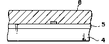
First, as shown in Fig. 3A and Fig. 4A, on the
15 substrate 4, which is made of a high temperature
resistant material such as hi~h-melting point glass, .
quartz, alumina, ceramias, etc. ,a thin film with
small nucleation density enabling selective nucleation
5 ~non-nucleation surface (SNDs)] i9 formed, and a
20 material dif~erent from the material forming the thin
~ilm 5 with small nucleation density is thin}y
deposited thereon, followed by patterning by
lithography, etc. to form sufficiently finely a
nucleation surface comprising a different
. .
25 material~SN~L) (or called "Seed") 6, thereby obtaining
~ a substrate for crystal formation. However, the size,
:: ,.,.. ~ ,
:, ~ : ..:
: . .
. :....
: ` :
- 18 - 13319~
1 the crystal structure and the composition of the
substrate 4 may be as desired, and it may be also a
substrate having a functional element already ~ormed
thereon according to conventional semiconductor
5 techni~ue. Also, the nucleation surfaces (SNDL) 6
comprising a different material is inclusive of -
modified regions formed by ion implantation of Ga, As,
etc. on the thin film S, as described above. -'~`~
Furthermore, the nucleation surface (SNDL) may be a
10 surface on which a nucleus can be substantially
formed, and is constituted of an amorphous material.
Next, by selecting appropriate ~eposition
conditions, a monocrystal of a thin film material is
formed only on the nucleation surface (SNDL) 6. That
15 is, the nucleation surface (SNDL) 6 is re~uired to be
formed sufficiently fine to the extent that only a
single nucleuæ may be formed. The size of the
; nucleation surface (SNDL) 6, which depends on the kind
o~ the material, may be several micrometers or less.
20 Further, the nucleus grows while maintaining a
monocrystal structure to become a monocrystal grain 7
shaped in an~island as shown in Fig.;3B. For the ;;~
island-shaped monocrystal grain 7 to be formed, the -
conditlons for crystal formation treatment are -~;
25 desirable to determine the conditions so that no ~ -
nucleation may occur at all on the free surface of
, ~ ' ., ,", '' ' ".',
''"~;',"' '~
- 19- ~3319$0 ~ :~
~ ~ :".,
1 the thin film 5.
The island-shaped monocrystal grain ~ further~:~
grows while maintaining the monocrystal ~tructure with
the nucleation surface ~SN~L) 6 as the center (lateral
5 overgrowth), whereby the thin film S can be partially
or wholly covered therewith as shown in Fig. 3C ;~
(monocrystal IA~
Sub~e~uently, the surface of the monocrystal
~A is flattened by etching or polishing to form a
10 monocrystal layer 8 on the thin film 5, by which a
- ,,:
- desired element can be formed, as shown in Fig. 3D or .
Fig. 4B.
Thu~, since the thin film 5 constituting the
non-nucleation surface (SNDs) is formed on the
15 ~ubstrate 4, any desired material can be used for the
substrate 4 which i9 the supporting member. Further,
in such case, even if the substrate 4 may be one
having a functional element, etc. formed by
semiconductor technique, a monocrystal layer 8 can be
20 ea~ily formed thereon.
In the above embodiment, the non-nucleation ~ ;
surface (SNDs) was formed with the thin film S.
However, as shown in Figs. 5A - SD, a substrate
comprising a material with small nucleation density
25 (ND) enabling selectiva nucleation may be used as
such, and a substrate for crystal formation may be
' ~:':' :
i . `
~ 20 - 1331950 ~ :
1 prepared by providing a nucleation surface (SNDL) at -~
any desired position thereof.
Figs. 5A - 5D are diagrams of the formation
steps of the crystal showing a second embodiment of
5 the present invention. As shown in Figs. 5A - 5D, by
forming a nucleation surface (SNDL) 6 comprising a
material with larger nucleation density (ND)
sufficiently finely on a substrate 9 comprising a
material with smaller nucleation density ~ND) enabling
10 selective nucleation to provide a substrate for
crystal formation, a monocrystal layer 8 can be farmed
thereon simil~rly as in the first embodiment.
Figs. 6A - 6D are diagrams of the formation
steps showing a third embodiment of the process for
15 ~orming the c~rystal according to the present
: ~ .
invention, and Figs. ~A and 7B are perspectiva views ~;
of Fig~. 6A and 6D,
As shawn in Flgs. 6A and Fig. ~A, on an
amorphou~ insulating material ~ubstrate 11, nucleation
20 surface9 (SNDL) 12-1, 12~2 are arranged su~ficiently
~inely with a material different from the material of
, the substrate 11 with a distance Q therebetween. The
distance Q may be set equal ta or greater than the
: ~ ,, :. .::
ize of the monocrystalline region required for ~-~
25 formation of, for example, a semiconductox element or ~ ;
~;~ a group of semiconductor elements.
: , . .:
:. :
~` : .. .
. .
- 21 - 1331950
1 Next, by selecting appropriate crystal forming
conditions, only one nucleus of the crystal forming
material is formed on only the nucleation surfaces
(SNDL) 12-1, 12-2, respectively. That is, the
5 nucleation surfaces (SNDL) 12-1, 12-2 are re~uired to
~: :
be formed to sufficiently fine sizes (areas) to the
extent that only a single~nucleus may be formed. The
sizes of the nucleation surfaces (sNDL) 12-1, 12-2,
which may differ dependin~ on the kind of the
10 material, may be preferably lO~m or less, more
preferably 5~m or less and =ost preferably l~m or
less. Further, the nucleus grows while maintaining a
monocrystal structure to become island-shaped ~rains
13-1, 13-2 as ~hown in Fig. 63. For island-shaped
15 monocrystal grains 13-1, 13-2 to be formed, as already
mentioned, it is desirable to determine the conditions
for crystal ~orming treatment so that no nucleation
will occur at all on other surfaces than the
nucleation sur~aces ~SNDL) on the substrate 11.
The crystal orientations of the island-shaped
monoarystal grains 13-1, 13-2 in the normal direction
of the substrate 11 are constantly determined so as to
make minimum the interface energy of the material of
. , ~: ...
:~ . . . .
the substrate 11 and the material formin~ the nucleus.
25 This is because, the surface or the interface energy
has anisotropy depending on the crystal face.
: .
.
~` ; ":
- 22 - 133~
1 However, as already mentioned, the crystal orientation
within the substrate plane o~ ~n amorphous substrate
cannot be determined.
The island-shaped monocrystal grains 13-1, 13-
5 2 further grow to become monocrystals 13A-1, 13A-2,
whereby adjoining monocrystals 13A-1, 13A-2 contact
mutually each other as shown in Fig. 6C t but since the
crystal orientation within the substrate plane is not
constant, a crystal grain boundary 14 is formed in the
10 middle portion between the nucleation surfaces (SNDL) -
12-1 and 12-2. ~ ~;
Subsequently, monocrystals 13A-1, 13A-2 grow
three-dimensionally, but the crystal face with slower
growth speed will appear as facet. For this reason,
15 flattening of the surfaces of monocrystals 13A-1, 13A~
2 is performed, and further the portion including the
grain boundary 1~ is removed, to form the thin films
15-1, 15-2 of monocrystals each containing no grain
boundary in shape of lattice as shown in Figs. 6D and ~ ;
20 73. The sizes of the monocrystal thin-films 15-1, 15-
2 are determined by the distance Q of the nucleation
surface ~SNDL) 12 as described above. That is, by
.:. - .
de~ining appropriately the ~ormation pattern of the
nucleation surface ~SNDL) 12, the position of the
25 grain boundary can be controlled to form monocrystals
. .
~ w~th desired sizes at a desired arrangement. ~
~: ,: ., .: .
~ ~ ' " ", ~ ' " ' ,,~:
~3~
1 Figs. aA - 8D illustrate the steps of forming
a crystal showing a fourth embodiment of the present
invention. As shown in the same Figures, similarly as
in the first embodiment is formed on a desired
5 substrate 4 a thin film non-nucleation surface (SND5)
5 comprising ~ material with smaller nucleation
density (ND), and a nucleation surface (SNDL) 12
comprising a different material with larger nucleation
:~ density thereon with a distance of Q to provide a .
10 substrate, whereby a monocrystal layer 15 can be
formed thereon in the same man~er as in the above
third embodiment.
Figs. 9A - 9C illustrate the steps of forming a ~ ~-
crystal according to the process of the present
15 invention showlng a fifth embodiment, and Figs. lOA
and lOB are per pective views in Figs. 9A and 9C.
Fir~t, a~ shown in Figs. gA and lOA, a
concavity 16 with desired size and shape i9 formed on
an amorphous insulating substrate 11, and a nucleation
20 surface (SNDL) 12 with sufficiently fine area size
capable of forming only a single nucleus i9 formed
therein.
Sub~equently, as shown in Fig. 9Br an isl~nd-
` shaped monocrystal grain 13 i5 grown in the same
25 manner as In the first embodiment. ~ ~:
And, ag shown in Figs. 9C and lOB~ the
~ :
- 24 - 1 331 9~o
1 monocrystal grain 13 is grown until embedding the
concavity 16 to ~orm a monocrystal layer 1~. -
In this embodiment, since the monocrystal
grain 13 grows within the concavity 16, the steps of
5 flattening and removing the grain boundary portion
become unnecessary.
Figs. llA - llC illustrate the steps of
forming a crystal showing a sixth embodiment of the ;-
present invention. As shown in the same Figures, on
10 any desired substrate 4 similar to the first . :~
embodiment, a thin film non-nucleation surface (SNDs)
18 comprising a material;with smaller nucleation -:-
density (ND) is forme~, and a concavity 16 with `~
desired size and shape is formed thereat. And, in the
~ ,, .: .
15 concavity is farmed in a fine area a nucleation
surface (SNDL) 12 comprising a material which is
different fram the material farming the non-nucleation
; surface (SNDs) and having larger nucleation density -
(ND), and a manocryctal layer 1~ is formed similarly
20 as in the fifth embodiment.
: ...~ :
Figs. 12A - 12C illustrate the steps forming a
crystal showing a seventh embodiment of the present
invention. A~ter a concavity is formed on a desired ~ :
bgtrate l9r a thin film non-nucleation surface -
25 (~SNDs) 20 comprising a material with cufficiently
small nucleation density (ND) is formed, and
.~ .
: ~ .
';~ ':'
f~ ^ 25 - 331 9S~ ~
1 following the same procedure as in the above
embodiments, a monocrystal layer 1~ can be formed.
Figs. 13A - 13D illustrate the steps of
forming a crystal showing an eighth embodiment of the
5 present invention.
Figs. 13A - 13C are the same as Figs. 6A - 6C. .
That is, a plural number (two in the Figures) of
nucleation surfaces 12 are formed with an interval of
Q to form monocrystal grains 13 subjected to
10 overgrowth on the nucleation ~urface 12. By growing - -~
further the monocrystal grains 13 to form monocrystal~
:: .
13A, a grain boundary 14 is formed at approximately
the center oP the nucleation surfaces (SNDL) 12, and
by flattenlng the surface of the monocrystal 13A, a ;-
15 polycrystalline layer 21 with grain sizes being -~
sub3tantially regularly Q as shown in Fig. 13D can be
obtained.
Since the grain size o~ the polycrystalline
. . .
layer 21 is determined by the interval Q between the
20 nucleation surfaces ~SNDL) 12, it becomes possible to
control the grain si2e of the polycrystal. In the
prior art, the grain size of a polycrystal was changed
depending of a plurality of factors such as the
formation method, the formation temperature, etc., and
25 when a polycrystal with a large grain size is to be
: . : . : .
~; prepared, it had a grain size distribution with a
:` :
,
- 26 - 1 331 950
1 considerable width. According to the present .-
invention, the grain size and the grain size
distribution can be determined with good
controllabilitv by the interval Q between the :~:
5 nucleation surfaces 12. :. -
, -,::
Of course, as shown in Fig~. 8A - 8D, the - ~ -
~; above polycrystalline layer 21 may be formed by `~--
forming a non-nucleation surface (SNDS) 5 with 9maller
nucleation denslty and nucleation surfaces (SNDL) 12-
10 1, 12-2 on a desired substFate 4. In this case, as ::~
..
already described, the polycrystalline layer 21 can be
formed with controlled grain slze an~ grain size -~
distribution without restrictions with respect to the ~ ~
material, structure, etc. of the substrate. - ~-
In the ~ollowing, specific processes for
forming the monocrystal layer or polycrystal layer in
the above embadimqnts are de~cribed in more detail. ~ : :
Example 1
, .
Referring to Fig. 14, the process for forming ~:
: 20 ~aAs film on 5iO2 is described as a first example of - ~
. ~ .
the present i~vention. :;` .
, First, on a substrate 4 made of a hi~h melting
glass, a SiO2 film 5 was deposited to about 1000 A by
the conventional CVD (chemical vapor deposition) by :;
25~use of silane ~Si~4) and oxygen~(02). The nucleation
~; density (NDs) of GaAs on the SiO2 film i5 small, and
,~, ,: .
..
:
~ ~ 27 - 1 9 ~ o
1 the SiO2 film 5 forms the non-nucleation surface
(SNDS). In place of forming a SiO2 film on the -
substrate 4, the substrate 4 per se may be constituted
of a material such as SiO2, alumina, etc.
Next, the surface of the SiO2 film 5 was
masked with a ph~toresist to a desired pattern.
By use o~ an ion implanter, As ions were
implanted to the side of the photoresist-masked SiO2
film. The As ions were implanted only on the surface
10 of the SiO2 film exposed CFig. 14A]. The amount -
implanted was 2.5 x 10¹⁶/~m2 or more. At the SiO2
: film surface where no As is implanted, the nucleation
density (NDs) o~ GaAs is small, and thi~ portion
becomes the non-nucleation surface ~SNDs). On the
15 other hand, the re~ions 12-1, 12-2 where As ions are
implanted have larger nucleation den~ity (NDL) than
the non-nucleation surface ~SND5), which portions
become nucleatlon surfaces ~SNDL). At this time, when
the size of the ion implantod portion was made 1.2 ~m
20 square. Thus, the substrate for formin~ a crystal was
prepared.
After the photoresist was peele~ off from the ~ ;;
SiO2 film, the substrate was subjected to he~t
~ .
treatment in a H2 atmosphere at ~bout 900 C for about
~; 25 lO minutes to clean the sur~ace.
Subsequently, while the substrate was heated
~: :
;- 28 -
: :. ,
1 to 600 oC, trimethyl gallium (Ca(CH3)3, hereinafter
referred to as TMG) and arsine (AsH3) at a molar ratio
of 1:60 were flowed together with a carrier gas H2 - i-
onto the substrate surface to grow a GaAs crystal ; ~-
5 thereon according to the MOCVD (organometallic ~ `~
chemical vapor deposition) ~ethod. The reaction
pressure was made about 20 Torr. This state was
maintained for a certain period, and then a single
nucleus was formed on each of the regiono 12-1, 12-2 ~ ~-
10 surfaces, and in each single nucleus the growth of a
single crystal started. Thus, as shown in Fig. 14B, ~. -
GaAs crystals 13-1, 13-2 was grown on the nucleation
sur~aces (SNDL) 12-1, 12-2 ~ormed by implantation of
As ions, and no GaAs cry~tal was grown on the non-
15 nucleation sur~ace ~SNDs), namely the SiO2 film
sur~aae where no As wa~ implanted.
Grawth of the GaAs cry~tals 13-1 and 13-2 were
~urther continued, and the GaAs crystals 13A-1, 13A-2
beaame to aontact each other as shown in Fig. 14C. At
20 that stage, the growth of the çrystals (interruption
of crystal forming, operation) was stopped. The
~ surfaces o~ the GaA~ crystals 13A-1 ahd 13A-2 were
; polished and the grain boundary was etched, and then `~
i
; GaAs crystals 15-1, 15-2 as shown in Fig. lgD were
25 obtained. A substrate temperature was 600 C and a
reaction pressure was 50 Torr.
. , :
`' ` ~'
i : ~
: ;.
/ - ~
^- 31950 ~ ~
. ~
1 The GaAs monocrystal 15-1, 15~2 thus obtained ~-
were evaluated by observation with an electron
microscope and X-ray diffraction. As the result, for
each of the monocrystals 15-1, 15-2, 50 x 100 GaAs
5 monocrystal, with grain size of 80 ~m and subtantially
without grain size distribution, were found to be
.. .::
formed on the substrate
All of these GaAs monocrystals are shown to :~
have monocry~tal characteristics of extremely good
10 guality.
..:
Example 2 ~:
Referring to Fig. 8, a second example of the
present invention i5 described
Fir~t, on the surface of a substrate 4 made of
16 ceramics, an SiO2 film 5 was deposited to about 1000 A
-
according to the thermal CVD method by use of SiH4 and
2'
. Next, by means of an arc di~charge type ion
platin~ device, on the SiO2 ~ 5 was deposited an
20 Al203 film. ~pon the deposition, after the device was
internally evacuated to 10 5 Torr, 2 gas wa~
introduced to 3 x 10 4 Torr in partial pressure, and
an ionization voltage was set at 50 V, a substrate -~
potential at 50 V and an output at 500 W. Thus, an
25 Al203 fllm was deposited to about 300 A on the SiO2
film 5. According to the electron ray diffraction
~ .
. .
.
~-~ 1 3 3 1 9 ,$ ~
- 30 - ~ ~-
1 analysis, the Al2O3 film was found to be amorphous.
With a photoresist masked to a desired pattern
on the Al203 film, the portion with the Al2O3 film ;~
exposed was etched with an etchant of ;~
5 H3PO4:HNO3:CH3COOH:H2O=16:1:2:1 to form nucleation ~-
surfaces 12-1, 12-2 (see Fig. 8A). At this time, the -~
substrate 4 was heated to abou~ 40 C. The si2e of . ~
the nucleation surface 12-1, 12-2 was made 1.2 ~m ~ -
square. Thus, the substrate for forming a crystal w~s
10 prepared.
Then, after the photoresist was peeled off, `
the substrate was subjected to heat treatment in a H
atmosphere at about '~00 C for about 10 minutes to
cle~n the surface. On the SiO2 sur~ace S, nucleation ~ ;
15 density tNDs) o~ GaAs is small, which portion becomes
the non~nucleation surface (SNDs). On the other hand, ~ ~
Al203 films 12-1, 12-2 have larger nucleation density ; ~;
~NDL) than the non-nucleation sur~ace ~SNDs) 5, which ~ ~;
portion become~ the nucleation sur~ace (~NDL)' -~
Subsequently, while the substrate was heated
to 600 C, trimethyl gallium (TMG) and arsine (AsH3)
at a molar ratio of 1:60 were flowed together with a
carrier gas H2 onto the substrate surface to grow a
GaAs ~ilm according to the MOCVD (organometallic
25 chemical vapor deposition) method. The reaction
pressure was made about 20 Torr. GaAs crystals 13-1,
~ 31 - 13~195~
1 13-2 were grown only on the Al2O3 nucleation surfaces
~SNDL) 12-1, 12-2, and no nucleu~ sufficient to grow a
crystal was formed on the non-nucleation surface
(SN~s) 5, namely the SiO2 surface.
Whe~n the crystal-growlng operation was further
continued, GaAs cr~ystals~of good ~uality were obtained
similarly as in Example l; A substrate temperature
was 600 C and a reaction pressure was 50 Torr.
Example 3
On the surface of a ~ubstrate resistant to
high temperature comprising ceramlcs, etc., an Al20
film was deposited to about 300 A by means of an arc
discharge type ion plating;device.
..: :
Next, a SiO2 film was deposlte~ to about 1000
15 A according to the thermal CV~ method by u~e of SiH4
and 2
With a photoresist masked to a desired pattern
on the SiO2 film, the portion of the SiO2 film exposed ~`
was etched according to reactive etching by use of
20 CHCl2F to form a nucleation sur~ace having a part of
the A1203 partially exposed. At this time, the
~ubstrate was heated to about 400 C. The size of the ~ ;
`;~ nucleation surface was made 1.~ ~m s~uare. Thus, the
sub trate for ~orming a crystal was prepared.
` ~ After the photoresist wao peeled off, the
. , .
~ substrate was ~ubjected to heat treatment in an H~ ~
~ 2 - 1 3 3 1 ~ 5 0 ::
1 atmo~phere at about soo C for about 10 minutes to
clean the surface. On the SiO2 film surface,
nucleation density (NDs) of GaAs is small, which
portion becomes the non-nucleation surface (SNDS). On ;
5 the other hand, Al203 film has lar~er nucleation ~-
density (NDL) than the non-nucleation surface (SNDS), ;
which portion becomes the nucleation surface (SNDL).
Subsequently, whlle the substrate was heated
to 600 C, trimethyl gallium (TMG) and arsine (As~3)
10 at a molar ratio of 1:60 were flowed together with a
carrier ~as ~2 onto the substrate surface to grow a
GaAs monocrystal according to the MOCVD
(organometallic chemical vapor deposition) method.
The reaction pres~ure was made about 20 Torr. A GaAs -
15 crystal was grown around its single nucleus formed ;~
.
only on the A1203 nucleation surface (SNDL), and such
a growth of a GaAs crystal was not found on the non~
nucleatlon surface (SNDs), namely the SiO2 film
surface.
0 When the crystal-growing operation was further
contlnued, GaAs crystals of good quality were obtained ;~
similarly as in Example 1. ~ -
xample 4
, ~
on a quartz sub~trate, a silicon nitride film
;~ ~ 25 w~o deposited to about 300 A thick according to the
;~ plasma CVD method. At this time, H2, SiH4 and NH3
~ ::
~: ".. . :,
~331950
- 33 -
1 were flowed at the ratio of 8:2:5, and a reaction
pressure was 0.16 Torr, RF power was lOW and a
substrate temperature was 300 C.
Then, patternin~ was performed with a -
5 photoresi~t. The slze of the silicon nitride film was
made 1.2 ~m s~uare. Remainlng small area of the
silicon nitride film becomes ~ nucleation surface and
, ~,
-~ the surface of the quartz substrate exposed becomes a ~.~
: ~
non-nucleation surface.
After the photoresist wa~ peeled off, the
substrate was subjected to heat treatment at about 900
~; C for 10 min. under H2 atmosphere to clean the
surface. Thus, the substrate ~or forming a crystal
was prepared.
While the ~ubstrate was heated to ~00 C,
trimethyl gallium ~TMG) and arsine (ASE3) at a mole
ratio o~ 1:60 were flowed together with a carrier gas,
~2 onto the ~ubstrate sur~ace~to grow a GaAs~film
according to the MOCV~ ~organometallic chemical vaper
20 deposition). The reaction pressure was about 20 Torr.
~aAs crystal was grown around its sing1e nucleus only ;~;
I , formed on the sllicon nitride nucleation surface
~SNDL). No nucleu~ for the growth~of a crystal was
not formed on the non-nucleation sur~ace,~ namely the
25 ~uartz ~urface. ~ ~
,, . ::
~; Example 5 ~
~:. .' '
~33195~
- 34 -
' ', ' ' ~
1 A GaAlAs mixed crystal III - V group compound
monocrystal was selectively formed as below.
After deposition of SiO2 film 5 to about 1000
A on a substrate 4 (hi~h melting glass) according to
5 the thermal CVD method by use of SiH4 and 2 in the
, .
same manner as iIl Example 1, with a photoresist masked -
to a desired pattern on the SiO film sur~ace, A3 ions
were implanted into the exposed SiO2 film at 2.5 x
.
1016/cm2 by use~of an ion~lmplanter. The slze of each i~
10 of the implanted regions 12-1, 12-2 was made 1.2 ~m ~ -
square. Thus, the substrate for forming a crystal was
prepared. -~
Next, the resist film was peeled off, and the
substrate was subjected to heat treatment in a H2
j 15 atmosphere at about 900 C for about 10 minutes to
clean the surface. ~ ;~
Also ~or the GaAlAs mixed crystal, the SiO2
portion implanted with no As ions has smalIer ` ~-
nucleation density ~NDs) to become the non-nucleation
j 20 surface (SNDs). On the other~hand, the portions 12
~; ~ 12-2 implanted with As ions have lar~er nucleation ~ `~
density (N~L) to become the nucleation surface (SNDL).
Onto the surface where the~nucleatlon surfaces
(SN~L) 12-1, 12-2 and ths non-nucleation surface
25 ~SNDs) thus havin~ a nucleation;~density dif~erence
ND) exist, by use of H2 as the carrier gas, TMG,
,~ :
: .
~: , : ,
3 3 1 9 ~ ~
- 35 -
1 trimethylaluminum (TMAQ) and AsH3 were ~lowed at a
ratio of (TMG+TMAQ):AsH3 of 1. 10 - 20 (molar ratio).
The substr~te temperature was made 800 C by heating.
The reaction pressure were made 30 Torr. Similarly as
5 shown in Fig. 14B, only on the nucleation surfacP
(SNDL) formed by implantation of As ions, the ternary
mixed crystal III - V group compound GaAlAs
monocrystal was formed selectively. When the crystal-
growing operation was continued, the monocrystals 13A-
10 1, 13A-2 were grown as shown in Fig. 14C. The slze of
each of the monocrystals was about 80 ~m, an~d the
crystallinity wao good. The~substrate temper~ture was
~50 C and the reaction pressure was 40 Torr. ~-
In this case, the ratio of Ga and As in GaAlAs ~ ~
15 can be freely controlled by vary~ng the ratio of the -
reactive gases TMG and TMAl.
As shown above in Examples, according to the
present invention, a s1ngle nuoleus is formed on a
nucleation surPace ~S~DL) of several ~m or less having
20 larger nucleation density (NDL), and a compound
semiconductor monocrystal belonging to the group III -
V of the periodic table can be grown only from the
single nucleus.
~ In the above Example~, there are shown ~ ;
; 25 examples in which SiO2 ~ilm~is formed by the GVD
.
~ method, but SiO2 film can be a1so formed according to .~ .:r;.~,,.~
:~: .:
~ ' ''~""
: ~ .
~331950
- 36 -
1 the sputtering method. Further, ~uartz itself with
its surface well flattened can be also used as the
surface on which a crystal is formed.
The ion species to be implanted for formation
5 of the nucleation surface ~SN~L) is not limited to As, -
:.
but ions of the group III elements, ions of the group
V elements, and further ions of the group II elements
and ions of the group VI elements can be also used.
As the III - V group compound, InP monocrystal
.
10 can be selectively formed on an amorphous substrate by ~
~,
use of trimethyl indium In(CN3)3 and phosphine PH3 as
the reactive gases, and AlSb monocrystal by uæe of
; :: :
trlmethylaluminum Al(CH3)3 and stibine SbH3.
According to combinations of the reactive gaseo as -
15 de~cribed above, monocrystals o~ GaP, GaSb, InAs, ~ ~
InSb, AlAs, AlP can be selectively grown, and further - '
mixed crystal III - V group compound monocrystal
according to any desired combination can be
selectively grown.
Also, the reactive gas o~ the group III
.
element is not limited to compounds having methyl
i ~ groups as described above, but compounds having ethyl
group~, propyl groups, butyl group~, isobutyl groups
such as triethylgallium Ga(C2H5)3, tripropyl indium
25 In(C3H7)3, tributyl gallium Ga(C4Hg)3,
triisobutylaluminum ~l~CH3)2CHCH2, etc. can be also
~:
`-` 13319~0 -
- 37 -
1 used.
The mixed crystal compound semiconductor can -
be selectively grown on the Al203 provided on SiO2
similarly as in Example 2 as the nucleation surfaae
5 (SN~L), as a matter of course.
Further, in the respective Examples as
described abo~:~e, there are shown examples in which the
MOCVD method i9 used in the stsp of selective growth -
of GaAs and G~AlAs monocry~tals, but selective growth
10 of the III - V sroup compoun~monocrystal can be
performed also according to the same principle by use
of the MBE (molecular beam epitaxy~ msthod, etc.
As de~cribed In detail above, the III - V ~ ;
group compound crystal article and the process for
15 forming the same according to the pre~ent invention,
by ~orming a nucleation sur~ace ~SNDL) of a material
having sufficlently larger nucleation density (ND)
than the material for ~ormation of non-nucleation ;
surface tSNDS~ ~u~ficiently finely so a g
20 a single nucleus, a monocrystal i9 grown selectively
at the site where the fine nucleation surface ~SNDL~) , r
exists, whereby a crystal such as a monocrystal with
necessary size, monocrystals shaped in a plurality of .
islands, a polycrystal with controlled grain size and
25 grains ~ize distribution, etc. can~be easily ~ormed on
: .
a base su~strate o~ any desired material. ~esid~s, no
:':` " ; ' ' ~`
13319~0
- 38 -
1 special new preparation device i5 re~uired, but it can
be forme~ by use of a device used in conventional
semiconductor process.
Also, the crystal according to the present
5 invention is not restricted with respect to the
material of the base substrate as in the prior art,
and therefore can accomplish easily three-dimensional
integration, are~ enlargement and lo~ cost. For
,:
example, since a monocrystal or polycrystal of III - V
10 group compounds can be easily~formed on an amorphous
insulating material, a multi-layer formation of an - ~,s
element with excellent electrical characteristics can ~ ;
be accomplished to realize an i~tegrated circuit of
multi-functions not found in the prior art. ~ ;
15 Specifically, it becomes poDsible to obtaln optical
element, surface acoustic element, piezoelectric
element, etc., and integration of each of them with
~ .... .
surrounding circuit IC, etc. Also, the present
:
Invention, when an inexpensive glass or ceramia is
20 used as the base material, can be applied for a large
area electronic device such as a large scale flat
panel display having the driving circuit integrat~ed on
one sheet o~ glass, etc.
Further, the present invention can form
.
25 monocrystals with necessary sizes~ at a plural number
of sites by forming ~he above nucleation surfa~es
: -
'~ ~ ` ;'
~' ' ' , ' '
l~3l~5~o
1 (SNDL) with desired sizes and desired intervalstherebetween on the non-nucleation surface (SND5),
whereby the formation steps can be simplified to a
great extent and also the formation time shortened, as
5 compared with the melting solidification method in
which monocrystal is formed by irradiation of laser or
electron beam.
~:~ AIso, by controlling the interval between the :
nucleation surfaces (SNDL) to be formed on the above ~ ~
10 non-nucleation surface (SN~S), a polycrystal .
controlled in its grain size through the interval can --~
be formed. The process for forming the polycrystal is ~ --
better in controllability of grain size and grain size
: .. , ~. -.. :. ~
distribution as compared with the process of the prior
15 art in which a polycrystal of a large grain size i9
~ormed accord~ng to the above melting solidificatian -~:r~
process, and also the ~ormation time can be shorte~qd
: to a great extent.
: "'~' '
'.: ,:
: 20 . :
,:,
.
,: . .
. . ~
~ : 25
~: -
: ~'"~'.' '