Note: Descriptions are shown in the official language in which they were submitted.
1332~
, ~ .
1 20104-8503
Switching network and switching network control
for a transmission system.
The invention relates to a switching network and a
switching network control for a transmission system.
In communication networks the portion of the data to be
transferred is ever increasing. To cope with the data traffic,
switching systems have been arranged separately for the data
traffic and the telephone traffic. Since the data rate of the
data signals to be transferred can assume a multiplicity of
different values, it is difficult ~o combine data and telephone
switching in one network node.
In the scope of the development of future, integrated
wideband networks discussions are held according to which method -~
the digital or analog information - partly requiring a large
bandwidth - is to be transmitted in digital networks. Packet
switching, in which the (digital) messages are segmented into
packets, have been known for a long time. Each packet contains
extra information in addition to the useful information; among
~ other things indications about the destination (address). On the -~
basis of their packet addresses the messages consequently allow to
be conveyed to the partner sharing the connection, which requires
transmission capacity only when a message is actually to be
! ' ' transmitted.
Furthermore, circuit switching has been known for a long
time, which requires transmission capacity for the total duration -;~
of the connection, irrespective of the fact whether messages are `~
just being transmitted or not. Specifically in the telephone
network, two-way transmission paths are made available, although
B
1~32~
la 20104-8503
in general only either one of the two telephone suhscribers is
speaking.
So far, the implementatlon of packet switching in data
traffic has led to transfer rates of the order of 1000 packets per
second and over. For future services that implement the method of
packet switching, for example in picture communication, a thousand
times this number is already calculated with nowadays. In order
to attain such transfer rates, the time consuming operation of
logging is separated
, :
' ;,'"'.'.''"
's' ' ~
; .,
:
1332~
PHD 87 289 2 15-11-1988
from the actual switching process in the case of Fast Packet Switching,
and the packets are divided over the transmission links according to
their destination addresses. Highly simplified logging that allows to be
rapidly evaluated is used to accelerate the switching process and the
switching networks. At the input of the switching node the arriving data
packets are processed decentralized, as they contain internal addressing
information which is in accordance with their destination, switched
through the central switching network and then transferred at the output
without the internal addressing information.
Embodiments for the UFast Packet Switching" are
~Asynchronous Time Division~ and ~Frame Relaying~. With respect to the
transfer mode a distinction is made between ~Synchronous Transfer Mode~
¦ and ~Asynchronous Transfer Mode~ as well as the mixing form ~Hybrid
Configurationc~. In the Synchronous Transfer Mode a specific
transmission channel is identified only on account of its distance in
I time from a synchronizing word. In the Asynchronous Transfer Mode each
channel is identified by the addresses ~headers) of its packets
I (blocks), especially the beginnings of the blocks can be recognized, so
that the headers can be evaluated. Flags or an inferior synchronous
structure are used supposing a constant block length. An example thereof
¦ is ~Asynchronous Time Divisionh, in which synchronizing words arerepeatedly blended into the bit stream as ~empty blocksH.
Especially hybrid configurations with a combination of
Synchronous Transfer Mode and Asynchronous Transfer Mode might gain
practical importance, because the network user wishes to continue to use
the already existing networks arranged in the Synchronous Transfer
Hode as long as possible on account of the high amount of the investment
costs.
In the European Patent Specification No. 0 183 592 a
30 wideband transmission system has been proposed, in which the message is `~
segmented into blocks (cells) and transmitted through wideband
transmission links according to an asynchronous time-division multiplex
method. The blocks (cells) can have the same or different lengths. The
blocks comprise useful as well as address lnfor~ lQn,~ whereas the
address information is accommodated in a so-called-header. The number of
bits of a block is designated as the block length, whereas the
standardization proposals in this context provide values between 120 and
`` 1 3 3 2 ~ O ~- !
3 20104-8503
256 blts for the useful informatlon and 32 or 16 blts for the
header. The tlme intervals, ln whlch the blocks are transmltted,
are designated as frames. A frame can comprlse a valld block or
be empty. Between two subscribers of the wideband transmission
system there ls a virtual connectlon whlch ls maintalned ln that
the blocks transmitted from the subscriber statlons are provlded
wlth unique header codes, which allow the switchlng nodes of
correctly conveying the blocks. The blocks arriving at the
swltchlng node of an incomlng line are transferred onto an out-
¦ 10 going llne after a conversion of the header. Since two or a
plurality of blocks may arrive for the same outgoing line durlng ~;
"
one frame, so-called queue buffers are to be provided in the ~'
swltchlng node. In the ~ueue buffer one or a plurallty of these
. ,,
blocks are temporarlly stored untll an empty frame is avallable
for them.
With respect to the buffer arrangement the swltching
nodes can be centrally buffered systems (for example, known from
the European Patent Speclflcatlon No. 0 183 592) or decentrally -
buffered systems. In centrally buffered systems there ls only one
buffer, ln whlch each incoming line dellvers lts arriving blocks
and whlch ls read agaln for these blocks by each outgolng line.
Systems havlng a decentralized buffering are further distinguished ;
! ~ ` , , .
by the fact whether a bufferlng of blocks takes place only on the
input slde or whether the buffers are excluslvely arranged for the ;
outgolng lines (compare, for example, IEEE, B 10.2.1, 1987, "The
Knock-out Switch: A Simple, Modular Archltecture for High-
Performance Packe~ Swltchlng" by J.S. Yeh et al) or whether
''~
':
':
3 ~
... .
.. ij 4 20104-8503
~ systems are concerned having an input and output bufferlng. In
~i?
; thls connectlon the term of Swltchlng Network Bufferlng ls also
~,~
used when a buffer is asslgned to each swltchlng point of a
swltching matrlx.
As shown ln the above embodlments, the arrangement of
~, the swltchlng network requlres extenslve lnvestlgatlons and care-
ful conslderatlon for a swltching node of a wldeband transmlsslon
system, ln order to take account of the multlfarlous dependence
and mutual lnfluences. In additlon, lt should be observed that
the swltchlng technlque for the swltchlng networks under dlscus-
slon verges on the llmlts of the present seml-conductor swltch
tlmes. Bottle-necks ln the performance can occur when various
blocks are slmultaneously transferred through the swltchlng
network of an exchange. The blocks can lnfluence each other when
ln the swltchlng network only few llnks are available as necessary
llnks. Two types of influenclng are especlally lmportant ln thls
connection: the conflict and the obstruction.
~` ~ Two blocks (or the circults transferrlng them) are ln a
mutually confllct~ng situatlon, when for the transmlsslon the same
~; 20 clrcuit components are to be used. As a rule, one of the blocks
~-~ wlll have prlorlty over the other, and the other block elther ls
to walt or be lost.
In case of obstruction, a block V ls to walt for the
¦~ processlng of a biock U, whereas simultaneously, however, U ls not
l~ processed because there ls a confllctlng sltuation between block U
~ ~.
and a thlrd block W. Consequently, a normal queulng sltuatlon ln
a queue buffer is no ob~ection, as long as the first block ln the
,":
X
~
13320~
4a 20104-8503
~;~ buffer i5 transferred at each frame clock Only when this buffer
,~ . .
ls in a conflicting situatlon and is not served, as a result of
which, however, no other block can be slmultaneously transferred
in this queue buffer, will there be an obstructlon.
The idea of obstructlon ls important for the evaluatlon :J
of the performance of such systems. Because, when a queue buffer
which ls not empty cannot be finished during a frame perlod, one
.can imaglne that an additlonal "vlrtual" block wlll be processed
instead. The sum of the virtual and real load is then the overall
load of the system. The virtual load in several switching
networks can nearly become as large as the real load. Thls ls
especlally true for the switchlng networks utlll~ing input
bufferlng.
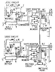
In Flg. 1 ls represented a swltchlng network havlng
lnput bufferlng.
From the hlghway system wlth supply llnes Z and trunk
: ` :
~`lines A a swltchlng network is structured ln the form of a space- ;
dlvislon multlplex swltching network. Each switchlng polnt CP
comprlses lts own evaluatlon loglc for the lnformatlon contalned
in the header. The blocks supplied through the supply line Z are
accepted on the lnput side to an lnput buffer B in the switchlng
network. The frames recelved
: . !
`,: ~.:.'
. ,
1332001
PHD 87 289 5 15-11-1988
from the subscriber or the preceding switching node are right-aligned in
the input buffer B By means of a comparator C assigned to each
switching point CP the addresses of the trun~ lines A arranged column-by-
column, which addresses are stored in the emfory SCA, are compared to
the routing information contained in the header To each of the trunk
lines A a decision circuit CA is assigned, which determines the order in
which the supply lines Z arranged line-by-line are to be switched in the
case of equal routing messages The order is determined by the spatial
arrangement of the supply lines Z, whereas each decision circuit CA
cyclically queries all its assigned comparators C
A number of shift registers SR corresponding with the
number of trunk lines A is connected to an input buffff~fr B, in which
registers the routing information is stored Each shift register SR is
connected to the switching point CP and also to the comparator C The
activating input of the assigned switching point is connected to the
comparator C through the decision circuit CA The decision circuit CA
~ controls, by eans of a signal provided by a logic circuit L, then ~ acceptance of a new routing message by the shift register SR The
signal is released by a release signal ALE applied to the logic circuit
L
The logic circuit L connected to the input buffer Bf
comprises a first AND gate U1 and a first OR gate 01 The first input of
the first AND gate U1 and of the first OR gate 01 of the logic circuit L
is connected to the decision circuit CA A start signal I produced in
the sffwitching node is applied to the second input of the first OR gate
01, whose output is connected to a reset input R of a bistable element
RS A data clock signal DC produced in the switching node is applied to
the second input of the first AND gate U1, whose output is connected to
the first input of a second OR gate 02 The inverting output of the
f i 30 bistable element RS is connected to a first input of a second AND gateU2, at whose second input a frame clock signal HC is present produced in
the switching node The output of the second AND gate U2 is connected to -~
the second output of the second OR gate, whose output is connected to
the input buffer B as well as the shift register SR An inhibit signal
f~ 35 DNH derived in the switching node from the frame clock signal
; NC is present at the set input S of the bistable element RS
; When the bistable element RS produces a switching signal
' .
~ :` 1 3 ~
6 20104-8503
at the invertlng output and the frame clock slgnal HC ls present
at the second input of the second AND gate U2, the header of the
flrst frame ln the lnput buffer B is read into the shift reglster
SR. The comparator C compares the routlng lnformatlon contalned
ln the header to the addresses of the trunk llnes A arranged
column-by-column contalned in the memory SCA.
.:,
In the case of correspondence the comparator C applles a
signal to the decislon circult CA and, on the basis of the recel-
ved slgnals, thls decislon clrcuit CA determlnes the order of the
supply llnes Z, arranged llne-by-llne which are to be swltched.
For thls purpose the decision circult CA applles the release slg-
nal ALE to the lnput buffer B and swltches the selected swltchlng
j polnt CP through. Wlth the ald of the data clock slgnal DC the
data D are swltched through the swltchlng polnt CP onto the trunk
llne.
For the case ln whlch no routlng lnformatlon ls contaln-
~ ed ln the header, the routlng lnformatlon stored in the shlft
j~ register SR ls not transferred to the trunk llne A.
~ Each swltchlng polnt CP comprlses a comparator C, whlch
¦; 20 compares the address of the trunk llne A, arranged column-by-
column, to the routlng lnformation. When there is multlple
correspondence ln one column, a decision circult CA asslgned to
the trunk line A determines the order in which the switching
polnts are tO swltch (Flg. 1).
For thls purpose an lnput buffer B is connected to each
supply line Z ln which buffer the blocks are temporarlly stored
untll they reach one of the trunk llnes A.
.
1332~
6a 20104-8503
As shown by extenslve experlments, hlgh loads may lead
to buffer overflow. Thls wlll be explalned herelnafter whlle
reference ls made to Flg. 2a for the sake of completeness. The
case wlll be consldered of an access confllct of a number of _
supply llnes Z and one trunk llne Al. The declslon clrcult CA
determlnes in whlch order the flrst blocks of the _ lnput buffers
B concerned reach the trunk llne Al. There ls one lnput buf~er Bk
(supply llne Zk) havlng the longest queue tlme: here the flrst
block Plk ls to walt ln the lnput buffer
1~ -
:: :
. ~ .,
'.:
.''''':
',''~',.
~ ~,
~332~1
7 20104-8503
il Bk for (n-1) block transfer times, until it reaches the line Ai
The second block P2k is to wait in this input buffer Bk for _
block transfer periods until it reaches its desired output line
Aj. This queue time specifically occurs when the output line A
was free for the duration of _ block transfer periods. In this
example it will become evident that free channel capacities remain
unused, which is then clearly noticeable at high loads.
! The invention has for its object to provide a switching
network as well as a switching network control for a transmission
¦ 10 system such that the occurrence of bottle-necks in the performance
i of the switching network is largely avoided.
~ The switching network is advantageous in that no rather
1~ large delays occur when the blocks are switched through the
switching network and conflicts are largely avoided.
The switching network control largely avoids the
disadvantages depicted above, because an input buffer is assigned
to each switching point. In the situation described with
reference to Figure 2b the input buffers Bik and Bjk both contain
the blocks P1k and P2k. The block P2k intended for the line Aj is
to wait for only one block transfer period before it can arrive at
the free line Aj, irrespective of the type of access conflict on
the line A..
According to a broad aspect of the invention there is
provided-an asynchronous time-division switching network, in which
network, blocks which include headers and data are routed to trunk ;
lines (Al...An) from supply lines (El...Em), based on routing
information in the headers, ~he network comprising~
a) a global clock source; ;~
~ ~32~
7a 20104-8503
b) a first number of interface units, which first number is
equal to a number of supply lines, each interface unit including
i) input means for receiving blocks as serial data;
ii) means for converting at least a portlon of the
serial data in a block to parallel form;
iii) means for providing a frame clock;
iv) means, coupled to the global clock source, for
elastically buffering the parallel form under control of the frame
clock; and
j~ 10 v) means for outputting contents of the means for
elastically buffering to an associated internal supply bus
(Zl...Zm) in parallel, frame-synchronized form;
c) the first number of the associated internal supply -
buses; and
d) a second number of concentrators, each for switching -~
data from a respective plurality of the internal supply buses to a
i respective one of the trunk lines, which second number is equal to ~
a number of the trunk lines, each concentrator comprising -`
i) the first number of input buffers for receiving ~j
~; 20 blocks from associated ones of the respective plurality of
internal supply buses in a form in which at least a portion of
~` each block is in parallel; ;
ii) the first number of means for comparing routing -
information in respective ones of the input buffers with an
~` address of the single trunk line;
iii) a decision circuit for determining an order of
transfer of data from the internal supply buses to the respective
trunk line, based upon results produced by the means for ;
d ~
7b 20104-8503
comparing;
iv) a multiplicity of junction points, so that when the
decision circuit determines transfer from a given supply bus,
bits, that are stored in parallel in the lnput buffer associated
with the associated internal supply bus, are transferred in
parallel from the input buffer to an internal trunk bus; and
v) means, having an output coupled with the single
trunk line, for converting data on the internal bus from parallel
to series for transmission to a respective trunk line.
According to another broad aspect of the invention there
is provided an asynchronous time-division switching network in
; which network, blocks which include headers and data are routed to
trunk lines (Al...An) from supply lines (El...Em), based on
routing information in the headers, comprising: ;
a) a global clock source; ~`
b) a first number of interface units, which first number is
equal to a number of supply lines, each interface unit including
i) input means for receiving blocks as serial data;
ii) means for converting at least a portion of the
serial data in a block to parallel form;
:
iii) means for providing a frame clock;
iv~ means, coupled to the global clock source, for
elastically buffering the parallel form under control of the frame ;`
clock; and
v) means for outputting contents of the means for ~;~
elastically buffering to an associated internal supply bus
(Zl...Zm) in parallel, frame-synchronized form;
c) the first number of the associated internal supply
~332Q~
`i`:
7c 20104-8503
buses; and
d) the first number of deconcentrators, each for
distributing data from a respective one of the internal supply
buses to a respective plurality of internal trunk buses, each
deconcentrator comprising
i) an input buffer for receiving blocks from the ~
respective supply bus in a form in which at least some of the bits :.
from each klock are in parallel;
ii) a plurality of comparators, one assoclated with
each internal trunk bus, for comparing routing information in the ~.
input buffer with an address of the trunk bus associated with that
internal trunk bus; and
iii) a multiplicity of junction points, such that there
is a junction point for each bit of each internal trunk bus, and
~ ...
so that when one of the comparators detects an address match, bits .;:;
; which are stored in parallel in the input buffer are transferred :
in parallel to the associated trunk bus. ~
The invention will be further described and explained~:
with reference to various embodiments shown in the drawing
Figures, in which~
Figure 1 shows an embodiment for a switching network
having input buffering, :
; Figure 2a and Figure 2b show for caparison the -:~
1- allocation of input buffers and switching network as shown in
: Figure 1 and Figure 3, :i;
Figure 3 shows an embodiment for a switching network :~
having switching network buffering, ;
Figure 4 shows a further embodiment for a switching
',"~.
d'~
~332~
. . .
7d 20104-8503
network having switching network buffering and
Figure 5 shows a further embodiment for a switching
network having input buffering when used as a concentrator.
,. ~
~ .
~ 1332~
PHD 87 289 8 15-11-1988
The embodiments for switching networks having an
expansion stage (deconcentrator) as shown in the Figs. 1 and 2a have
already been extensively discussed. These switching networks can be
built up of identical structural elements B~ so that the switching
S network is segmented ~column-by-columnH. The data of the supply lines Z
are preferably offered to all units BE in parallel with a bus-like
cabling (see Fig. 3~. The transfer from the supplyline Z to the bus-like
cabling is performed by interface circuits IM.
Each interface circuit IM comprises, besides functions
for a serial-to-parallel conversion of the data, a buffer circuit P
with which all incoming data are synchronised with a header. The ~
interface circuit IM and structural elements E are preferably designed ~;
as plug-in cards for a back wall wiring, with which the bus-like cabling
can be realised in a very advantageous way.
Fig. 4 shows for a switching network with switching
network buffering (structural component having input buffering) a
switching network control, in which the function of the circuit
components used was already extensively discussed with reference to
Fig. 1. In the highway system arranged in the way of a space-division
multiplex switching network a number of input buffers B corresponding
with the number of trunk lines (A) are connected to each supply line Z,
in which buffers the supplied blocks are temporarily stored. To the bus
line on the output side of an input buffer B is connected a comparator C
assigned to the switching point, which comparator compares to the
routing information the addresses of the trunk lines A arranged column-
by-column and stored in the memory SCA. In the case of multiple
correspondence the decision circuit CA, connected both to the
comparators C and to the switching points CP, determines the order of ;~
the supply lines Z arranged line-by-line which have to be switched
through.
Each comparator C is connected to a flipflop FF to whose
inverting output the switching point CP and to whose non-inverting
output the decision circuit CA is connected. ~
, ~ - .,
After the evaluation of the routing inf~rmat;ionby the
comparator three cases are to be distinguished:
1. The block P1k is intended for the trunk line Al and the trunk -~
line Al is assigned thereto by the decision circuit CA. In this case ~
'~,: .;;
3 2 ~
PHD 87 289 9 15-11-1988
the switching point CP switches and the block P1k is read from the
input buffer ~ (triggering of line ALE).
2. The block P1k is intended for the trunk line Al and the line Al
has not yet been assigned thereto by the decision circuit CA. This is a
5 condition of queueing until the trunk line Al is assigned ~compare 1). -
3. The block P1k is not intended for the trunk line Al. There is no
signal from the decision circuit CA. The line ALE is triggered via the
inverting output of the flipflop FF. The block P1k is read out but
does not reach the trunk line Al via the switching point CP.
The decision circuits of the Figs. 3 and 4 define a
declining priority of the supply lines 1, 2, ... with buffers that are
not empty.
In order not to implement the decision algorithm in an
unfair way, this establishing of priorities should be different for each
structural element BE, roughly in the following way:
Trunk line Declining priority of the supply lines
1 1, 2, 3,
2 2, 3, 4,
3 3, 4, 5,
A structural element BE can be advantageously used as a
concentrator: it then causes the data streams of _ lines to be
; concentrated on one line. For the opposite direction a further component
is then required, which is represented in Fig. 5. It allows to transfer
the data coming from a supply line Z to n trunk lines A according to
their routing information: This corresponds with the function of a
demultiplexer.
Since no access conflict can occur, the decision circuit
CA is cancelled. The components from Fig. 3 can also operate as a
statistical multiplexer: In this case the comparator C is to show that
one block anyhow is available in the supply line Z concerned.