Note: Descriptions are shown in the official language in which they were submitted.
~ 1332026
TITLE OF THE INVENTION
Superconducting Wire and Nethod of Manufacturing the
Same
BACKGROUND OF THE INV~NTION
Field of the Invention
The present invention relates to a method of
manufacturing a superconducting wire, and more
particularly, it relates to a method of manufacturing a
superconducting wire of a ceramic superconductive material.
Description of the Prior Art
Metal and ceramic superconductors have generally been
well known in the art, and have been studied for various
uses. A superconductor loses all resistance to electric
current when held at a temperatura below its critical
temperature. Through this property, attempts have been
made for generation of high magnetic fields and high
density transmission of large currents.
~;~ In order to use a superconductor for generation of a
high magnetic field or high density power transmission, it
is necessary to provide the same in the form of a thin ~``
wire. Also in applications other than the above,
~ superconductive wires are required. Although known metal
`! ~ , ; superconductive materials can be easily worked into wires,
the critical temperatures thereof are quite low, (e.g.,
lower than about 23 K), which restricts the cooling mediums
' ~
B ~
.
133~026
that can be employed, whereby their application is
extremely limited.
On the other hand, some ceramic superconductive ~-
S materials have high critical temperatures. However, it is -;
extremely difficult to work such ceramic superconductive
materials into wires. Even if the materials are worked
into wires, it is extremely difficult to provide stable
electrical properties over the entire length thereof.
In general, a wire rod of ceramics superconductor is
manufactured by:
(1) performing cold working at the normal ~-
temperature; or
(2~ heating the material to a temperature for
facilitating plastic working.
In the case of the method (1), wire drawing of the raw
material of the ceramic superconductor tends to be non-
uniform, causing disconnection of the superconductive
portion of the wire; hence the fineness of the wires is ;
restricted. Further, even if the superconductor is worked
into a wire of considerable thickness, the electrical
properties there of are degraded to some extent.
In the case of the method (2), a raw material for the
ceramic superconductor is generally placed in a metal pipe
to be heated to a high temperature and thereafter extruded
into the form of a wire, to be further subjected to wire
drawing by a die or the like, if necessary. Thus, the raw
- 2 - ~;
B ::~
1332026
material for the ceramic superconductor is sub~ected to
heat treatment in a state isolated from the external
atmosphere by the metal pipe, which prevents exposure to
elements required to form the superconductor, such as
oxygen. Thus, the superconductor cannot be provided with
the expected critical temperature and critical current.
Further, the degree of fineness of the wire rod is
, . .
restricted.
Ceramic superconductive materials have recently gained
prominence as they can perform at increased critical
~ .
temperatures. Such superconductive materials can be shaped
into elongated linear bodies, for example, to be applied to
uses such as power transmission/distribution, electric
connection of various devices or elements, winding for a
coil, and the like. ~-;
It i8 known that ceramic superconductive materials ~
. ~,
such as Y-Ba-Cu-O, for example, of perovskite or pseudo~
perovskite structure, superconduct at high critical
temperatures.
SUNMARY OF THE INVENTION
An ob~ect of the present invention is to provide a
method of efficiently manufacturing a superconducting wire
o$ a ceramics superconductive material composed in design,~ -
~ 25 which can be increased in critical temperature and worked
`~ 3 - -
"~
1332026 ~
into a wire rod with no degradation in electrical property, ~-and a superconducting fine wire obtained by the said
method.
Provided according to the present invention is a
method of manufacturing a superconductive wire composed of
a ceramic superconductive material of composition -
AaBbCucOd, wherein ~ is at least one of Y, La and Bi, B is
at least one of Ca, Sr, and Ba, and a, b, c and d represent
the relative molar ratios of A, B, Cu and O. -~
According to the inventive method of manufacturing a
superconductive wire, a raw material precursor of the
ceramic superconductive material is first prepared. The
material is melted in a vessel having a hole in
communication with its interior, to obtain a melt. The
melt is linearly discharged from the hole by either ~;
extrusion or drawout and the linearly discharged melt is
cooled and solidified to obtain a solidified body. This
melt may be solidified by forced cooling or natural -
standing. Further, at least a single vitrifying compound
such ac B2O3, GeO2 or P2Os may be added in the step of
melting the raw material, in order to bring the melt into a
highly viscous glassy state. In this case, the solidified
body as obtained may be crystallized by further re-heating. ;
According to the aforementioned method of
manufacturing a superconducting wire rod, the ceramics ~ ;
superconductive material can be brought into a considerably
- 4 -
B
1332026
viæcous state through melting in a heating vessel. Thus, a
superconducting wire rod can be obtained by extruding or
drawing out the melt from the hole. Since the melt is
extruded or drawn out in the considerably viscous state,
the wire rod can be very thin, equal in diameter to the
size of the hole.
Thus according tO the present invention, a
superconducting wire rod is manufactured by melting a
ceramic superconductive material and extruding or drawing
out the same, whereby a superconducting wire rod having a
high critical temperature and excellent electrical
properties can be obtained by a simple method.
In the aforementioned melting-cooling/solidifying -~
method according to the present invention, it is difficult
to obtain a ceramic superconducting wire being composed in
design even if the raw material is correctly prepared in
composition. The composition of the ceramics ~`
superconducting wire is subject to fluctuating due to
dissociation and recoupling of elements contained in the
raw material while in the molten state. In consideration
of this, the inventors have found out that a ceramics
superconducting wire can be reliably manufactured by
ad~usting the atmosphere in which at least one of the steps
is performed, in particular the melting and
cooling/solidifying steps.
B
.:,
: ~
~33~2026
According to the inventive method of manufacturing a
superconducting wire, a raw material of composition
AaBbCucCXcx is first prepared, in which cx represents at
least a single element selected from oxygen, carbon,
nitrogen, fluorine and sulfur and cx represents a number
showing the composition ratio of CX.
According to this manufacturing method, the material
expressed as AaBbCucCXcx is first melted. The method
further comprises at least a step of linearly discharging ~:
the melt obtained by melting through extrusion or drawout
and a step of cooling and solidifying the linearly
discharged melt.
This manufacturing method may comprise at least the :
melting step, the discharging step and the ~ `.
cooling/solidifying step, and hence some steps may be
freely performed after the melt is solidified.
Further, the inventive manufacturing method is ~ ;
characterized in that at least one of the entire steps
including the aforementioned melting, discharging and
cooling/solidifying steps iB performed under an atmosphere
;~: containing a CY component of partial pressure being higher
than CY partial pressure in the atmospheric air. The CY
: component is prepared by a gas containing at least a single `~
element selected from oxygen, nitrogen, carbon, fluorine : :
- 6 - ;
' .' .
''' ~3 ;~
~33202~
and sulfur. Examples of the CY gas are oxygen, nitrogen,
carbon monoxide, carbon dioxide, hydrogen fluoride and -
hydrogen sulfide.
S The aforementioned atmosphere in which CY partial
pressure is higher than that in the atmospheric air may be
introduced into "at least" one of the entire steps. Thus,
only the melting step may be performed under the said
atmosphere, while only the cooling/solidifying step may
alternatively be performed under the said atmo~phere. The
melting step or the cooling/solidifying step is so
performed under this atmosphere that melting or
cooing/solidification is carried out in an atmosphere being
rich in CY.
The material may be re-heated after the ~
cooling/solidifying ætep under an atmosphere in which CY ~-
partial pressure is higher than that in the atmospheric
air. ~ ~
It is pointed out that the material expressed in the~ -
~, . .
aforementioned general formula AaBbCucCXcx can be prepared ~-
by a partially fabricated item whlch is not completely
superconductive, in addition to a mixed body and a compact.
Thus, according to the present invention, an element
which is easily dissociated or changed in a molten state ~;
can be prevented from such dissociation or change by ;;
adjusting an atmo~phere introduced into a part of the
',~' ';:
- 7 - ~
, ~.
~ '. ~'"~ ' .
.
~3321026 :~
manufacturing steps, while an element not contained in the ..
raw material can be supplied from the aforementioned
atmosphere as the case may be. Thus, a ceramics
superconducting wire can be reliably composed in design.
It is pointed out that the inventive manufacturing
method is applicable to a method of manufacturing a~:
ceramics superconducting wire which is employed for
':
,:
. .
.~ ~; / " ', .:.
~ 8 -
~ ~r-B ~
; ~
1332o26
general application of such a superconducting wire, in
addition to that employed in the field of energy such as a
high current density magnet or a long-distance
transmission line or an electronic device such as a
5 Josephson device. ~;
The present invention is further directed to a method
of manufacturing a superconducting wire comprising the
steps of melting a ceramics superconductive material in a
vessel heated to a temperature exceeding the melting point
thereof and extruding or drawing out the molten
superconductive material from a hole communicating with
the interior of the vessel to cool/solidify the same.
This method is characterized in that the
cooling/solidifying step is performed in a space being at `~
a temperature between the solidifying point of the
superconductive material and a temperature lower by 100C ~
than the solidifying point. ~;-
According to the present invention, a ceramics
superconductive material being molten in a vessel is
20 discharged from a hole communicating with the interior of ~;
the vessel to be cooled/solidified. The
cooling/solidifying step is performed in an atmosphere of `~
a temperature close to the solidifying point of the
superconductive material, i.e., at a temperature level
~5 between the solidifying point and that lower by 100C than ;
~`~ 9 ~ ;`
B :~
1 332026
the solidifying point, thereby to reduce thermal
distortion caused in solidification of the molten
superconductive material. Therefore, an elongated
superconducting wire can be manufactured in high
productivity with no breaking in or upon solidification of
the molten ceramics superconductive material. If the
temperature of the space for performing the
cooling/solidifying step is less than the temperature
lower by ~00C than the solidifying pointl an elongated
superconducting wire cannot be re`adily obtained and the
solidified superconducting wire is easily broken. It has
been also confirmed by reduction in critical temperature
that, if the said temperature is less than that lower by ;~
100C than the solidifying point as described above, the
: 15 cooledJsolidified ceramics material is not brought into
desired perovskite or pseudo-perovskite structure, or the
ratio of such crystal structure is reduced. The
temperature of the space for carrying out the
cooling/solidifying step is preferably selected to be
closer to the solidifying point of the superconductive
material, i.e., at a temperature level between the
solidifying point and that lower by 50C than the
solidifying point in order to further reduce thermal
distortion caused in solidification, thereby to further
effectively manufacture an elongated superconducting wire
: . /0
B ::
1332026
of a ceramics superconductive material being in desired
perovskite or pseudo-perovskite structure.
Preferably a zone next to the space for performing
the coolinglsolidifying step is provided to be at a -
relatively high temperature in a portion closer to the
hole of the vessel while having a temperature gradient
along a direction for linearly discharging the melt, so
that the cooled/solidified superconducting wire is passed
through the zone to be slowly cooled. Desired perovskite
pseudo-perovskite structure can be further excellently
attained in a superconducting wire thus obtained. This
~: .
~: has been confirmed by measurement of a critical
temperature. Particularly in slow cooling of the
superconducting wire, an average cooling rate is
preferably selected to be not more than 10Ctmin. at least
until the temperature reaches 200C.
These and other objects, features, aspects and
advantages of the present invention will become more ~-
apparent from the following detailed description of the
present invention when taken in conjunction with the
accompanying drawings.
BRIEF DESCRIPTION OF THE DRAWINGS
Fig. l is a schematic process diagram showing a
method of manufacturing a superconducting wire according
~ , ~
~ 25 to the present invention se~uentially along steps;
B
. ::
.
:~
1332026
Fig. 2 is a schematic block diagram showing an
embodiment of an apparatus for manufacturing a
superconducting wire rod based on the inventi~e
manufacturing method; and
Fig, 3 is a schematic block diagram showing another
embodiment of the inventive manufacturing method.
DESCRIPTION OF THE PREFE~RED EMBODIMENTS
~; Fig. 1 is a process diagram schematically showing a
method of manufacturing a superconducting wire according
to-t-he-present invention. Referring to Fig. 1, a raw
~; material of prescribed composition is first prepared in
the form of powder, a compact or the like. This raw ~-
material is molten in a vessel having a hole provided to
communicate with its interior. A melt thus obtained is
; 15 linearly discharged from the hole through extrusion or
; drawout. The linearly discharged melt is thereafter
`; cooled to be solidified. Thus, a superconducting wire of
prescribed composition is obtained in the form of a
solidified body.
The inventive method of manufacturing a
superconducting wire is now described with reference to
Examples.
Example 1
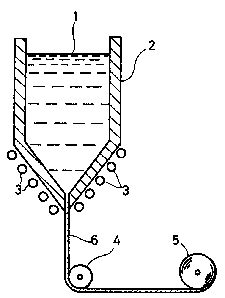
;~ Fig. 2 is a schematic block diagram showing an
-~ 25 embodiment of a superconducting wire rod manufacturing
:~ - B ::
1332026 ~
apparatus for carrying out the present invention. A
heating source 3 is provided in proximity to an extrusion
port of a heating furnace 2 containing powder of a
ceramics superconductive material 1. Further provided are
a guide roll 4 for guiding a ceramics superconducting wire
extruded through the extrusion port and a take~up roll 5 ~.
for winding the ceramics superconducting wire. .
In more concrete terms, powder of Y2O3, BaCO3 and CuO
mixed in the ratio 0.2:0.6:1 was preliminarily sintered at -~
900C for 10 hours and pulverized to prepare the ceramics
superconductive material 1, which could be brought into a ~:
:: half-molten state by raising up the inner temperature of
the heating furnace-2 to 1000C by the heating source 3.
The ceram.ics superconductive material 1 was extruded
from the extrusion port to be wound on the take-up roll 5
through the guide roll 4, thereby to obtain a fine wire 6
of 100 ~m in diameter. ~
Sharp superconductivity transition was observed in .
the superconducting fi.ne wire 6 thus obtained, with a :
`~ 20 critical temperature of 90 K and critical current of 20 A.
Thus, a superconducting magnet having a high critical ~.
. temperature and excellent electrical properties can be
implemented through the superconducting fine wire obtained
in the aforementioned manner. Alternatively, a
25 superconducting transmission cable having a high critical . ;
~: ~3
B `
',':'~
1332026
temperature and excellent electrical properties can be
implemented through the superconducting fine wire.
In order to form such a superconducting magnet or
superconducting transmission cable, a stabilizing material
such as copper is preferably adapted to hold or be held by
a large number of fine wires, to prevent heat generation
in quenching for transition into normal conduction as well
as to prevent burning of the superconducting fine wires.
The present invention is not restricted to the
aforementioned Example but a ceramics superconducting
material can be molten in a coarsely crushed state or the
diameter of the wire rod can be set in a desired value
other than 100 ~m. Further, various modifications may be
introduced in design within a scope of the present
invention.
Example 2
;A mixture of Y203, BaC03 and CuO was molded and
previously subjected to heat treatment, to be
~ heated/molten in a crucible under an atmosphere containing
`~ 20 oxygen of 200 Torr. Then the melt was drawn out from a
nozzle of 500 ~m in bore diameter, to be solidified in the
` form of a~fine wire. The fine wire thus obtained was made
of a ceramics superconductive material composed of
Y0 4BaO 6CuO22,which superconducted at 90 K.
Example 3
- ~ ~
B
: ,:
~332026 ~ `
A material being in average composition of
La1 6SrO 34CuO4 containing 0.01 wt.% of fluorine was
molten in a crucible under an atmosphere containing SF6
gas of 100 Torr., to manufacture a tape-like member of 30
~m in thickness and 60 mm in width similarly under an
atmosphere containing SF6 gas of 100 Torr. by the
so-called roll quenching method. This tape-like member
superconducted at 40 K.
Example 4
The material obtained in Example 2 was heated under
an atmosphere containing oxygen of 200 Torr. at 1100C for
two hours, to obtain a ceramics superconductive material
of Y0 4BaO 6CuO2s. This ceramics superconductive material
superconducted at a temperature of 95 K.
Example 5
~;~ Fig. 3 illustrates a state of carrying out Example 5.
~;~ A ceramics superconductive material 11 of YBa2Cu3O7 ;~
having a solidifying point of about 109~C was molten at a ~
temperature of 1180C in a platinum crucible 13 heated by ~;`
-~20 a heater 12. The molten ceramics superconductive material
11 was drawn out from a hole 14 provided on the bottom
wall of the crucible 13 to be cooled/solidified, thereby
to obtain a superconducting wire 15.
~-~The space for performing the aforementioned
cooling~solidifying step was enclosed by a tunnel 16, for
:
B ~
, ~ ,
1 3320~6
example, and provided with a prescribed temperature
atmosphere by a heater 17 arranged in relation to the
tunnel 16. Namely, the tunnel 16 was provided in its
relatively upward portion with a coolinglsolidifying space
18 being brought into a higher temperature atmosphere,
while a slow-cooling zone 19 was formed in communication
with the cooling/solidifying space 18. The
cooling/solidifying space 18 was set at a temperature of
1080C, while a lower end of the slow-cooling zone 19 was
set at a temperature of lOS0C.
The superconducting wire lS discharged from the
tunnel 16 was drawn out through a pair of rollers 20 and
21 rotated along arrows in Fig. 3.
The superconducting wire 15 thus obtained was ~0 ~m
lS in diameter~ and superconducted at a critical temperature
of 85 X.
Reference example was prepared by the same
superconducting wire 15 to draw out the same while
stopping heating by the heater 17. However,`the
superconducting wire 15 was occasionally broken.
A superconducting wire obtained by the inventive
method is` not restricted to that of a circular section.
The sectional configuration of the superconducting wire
depends on that of the hole 14 provided to communicate
with the interior of the crucible 13, and a
/6
B
1332026
superconducting wire of an arbitrary sectional
configuration, such as a tape-like one, can be obtained by
changing the configuration of the hole 14.
Example 6
Respective powder materials of Bi2O3, SrCO3, CaCO3
and CuO were weighed so that Bi, Sr, Ca and Cu were in the
composition ratio 1.1:1:2 and mixed with each other to be
temporarily fired in the atmospheric air at 800C for
eight hours, thereby to prepare raw material powder to be
molten.
This powder was introduced into a crucible to be
molten, drawn out and solidified in the atmospheric air
through the apparatus as shown in Fig. 3, thereby to
obtain a fine wire of 100 ~m in diameter. This fine wire !,
15 was annealed in the atmospheric air at 830C for eight ;~
hours, and thereafter slowly cooled. ~'he critical
temperature TC of the fine wire thus obtained was measured
through measurement of electric resistance by a general
four-terminal method. This fine wire was in such
superconductivity that its electric resistance reacned
zero at 100 K.
! I i Example 7
A material obtained by adding B2O3 of 20 % in mole
ratio to a ceramics superconductive material composed of
Y1Ba2Cu3O7 x was introduced into a crucible to be molten,
/ ~Z '.
_,~- ~ ~
B :
1332026
drawn out and solidified in the atmospheric air at 800C
through the apparatus as shown in Fig. 3, thereby to
obtain a fine wire of 50 ~m in diameter. This fine wire
was in a partially crystallized glassy state. Then the
fine wire was annealed in the atmospheric air at 700C for
six hours, and thereafter slowly cooled. The critical
temperature TC of this fine wire was 8~ K.
Although the present invention hzs been described and
llustrated in detail, it is clearly understood that the
10 same is by way of illustration and example only and is not ~ ::
to be taken by way of limitation, the spirit and scope of
the present invention being limited only by the terms of
~:; the appended claims.
B
~ ....