Note: Descriptions are shown in the official language in which they were submitted.
1332~27
. ::
JITTER CONTROL IN DIGITAL COMMUNICATIONS LINRS ~-
This in~sntion relstes to ~itter control in
digital communication~ links.
More particularly, the inYention relates to --:
jitter control in a chain of asynchronous ~igital
communications links.
Communications networks frequently inclu~e a
chain of nodes N interconnected by links. One such
arrangement i~ ~isclosed in International Publication
No. WO 86~03639. Digital informaton starts at node
Nl and is relayed, with or without mo~ification to
its content, successively by noaes N2, N3,... In
the case of the three typical ad~acent nodes Ni 1
Ni, Ni~l, information is transmitted at the rate
f fi 1 bits per second from Ni_l to Ni, at the
e fi fro~ Ni to Ni+l. The rates...fi 1
fi, fi~l...are nominally the same, but are
dictated by separate clocks, respectively in nodes
.
.
", j.
~ 1~32~27 ~
Ni 1~ Ni~ Ni~l, and therefore differ from each
other by unpredictable and varying, even if small
amounts.
One known practice to avoid these variations
is to operate such a chain synchronously without a
local clock wherein the only autonomou~ clo~k is in
Nl and the ~lock~ in N2, ~3,... are slaved to
it. The ~laving is typically done by a technique
known as bit elock estraction whereby each node
synchroniæe~ the rate and phase to the incoming bit
stream. It then uses the same clock to form and
transmit the outgoing ~tream. There i8 an ever
increasing ~ifficulty with thi~ approaeh as the chain
is made larqer. Cloek estraction is ~ub~ect to a
finite amount of ~itter i~ pha~e and the ~itter
accumulates from node to node lea~ing to a
progressively increasing ineidence of bit errors.
T~e use of in~epend3nt elock~ in the no~es
i~ another known teehnigue for overeoming the phase
jitter problem. An e~traeted eloek i8 still used on
the receiving side of the node, but the transmi~ion
is by an in~ependent eloek and therefore not affeeted
by the jitter in the reception. 8ueh an arrangement
is made possible by making all transmissions at a
higher rate than would be n~cessary to transmit the
actual data and by a~ding stuffing bits into the
stream. The number of stuffing bits over a f~sed
interval of time can vary from lin~ to link, the
differences eompensating for the differences in ~loek
rates. 8y deletion or in~ertion of ~tuffing bits or
groups of bits, the ela~t~e buffers are not allowed
to overflow or go empty.
The digital information iæ generally
formatted, and generally into frame~ of fised numbers
.
; .. . . . .
. ,., . , , ~.
~;~ 1 3 ~ 7
3 23199-115
of bits, the frames recurring at nominally fixed lntervals. To
allow for stuffing, the format must provide space for stuffing
bits. Typically this can be the residual time interval between
the end of data of one frame and the beginning of the next frame.
Since the number of stuffing bit~ is variable, there i5 the
further requirement that there be a definite indication of the
start of the frame.
Generally speaking, the object of the present invention
is to overcome drawbacks in the known techniques.
One problem is in the size of fluctuation of the
stuffing space in any frame and hence time jitter in the
occurrence of the frame marker at all nodes of the chain. The
existing practice is that stuffing bits are deleted or inserted by
a node on the sole indlcation provided by the state of fill in the
elaætic buffer in that node. Whlle this functions quite well most
of the time and on average glves satisfactory performance, in a
system with a large number of nodes it is sub~ect to occasional
large variations in the number of stuffing bits in individual
frames. Moreover the size of the possible fluctuation grows
linearly with the number of nodes. In accordance with one aspect
of the invention the size of the possible fluctuation is held to a
designated maximum lndependently of the number of nodes.
In accordance with the present invention, there is
provided a method of transmitting digital signals (DI) in frames
which include a stuffing field between nodes (N) in a network,
each node having a buffer and a local clock for producing local
clock signals (CLK2), said method including the steps of:
extracting clock signals (CLKl) from the digital signals (DI);
~3
4 1332~ 23199-11S
writing sald digital signals (DI~ into the buffer at the extracted
clock signal (CLKl) rate; reading said digital signals (DI) from
the buffer at the local clock signal (CLK2) rate, including
reading the content of the stuffing field in order to add or
subtract stuffing bits therein in order to compenæate for
differences in frequencles between the local and extracted clock
signals (CLK2, CLKl); controlling said adding or subtracting of
the stuffing bits so that the length of the stuffing field is
within predetermined limits, wherein each of the frames includes a
stuffing control field and addltion or subtraction of the stuffing
bits is controlled in accordance with an unconditional stuffing
control code (F0, Fl) in the stuffing control field, which
indicates the length of the stuffing field; monitoring frame
markers (FMI, FMX) for frames ups~ream and downstream of the
buffer, generating phase difference slgnals from said markers
(FMI, FHX) and generating conditional stuffing control codes (C0,
Cl) ln accordance with the variation between the phase difference
signals and a desired phase difference value (D) between said
frame markers (FMI, FMX); and generating the uncondltional
stuffing control codes (F0, Fl) by comparing the potential length
of the stuffing field if varied in accordance with said
conditional stuffing control codes (C0, Cl), and determining the
value of said unconditional stuffing control codes (F0, Fl) such
that the length of the stuffing field (lOJ is not outside
predetermined maximum and minimum lengths.
In accordance with the present invention, there is
further provided apparatus for transmitting digital signals (DI)
in frames which include a stuffing field between nodes (N) in a
.~ ~
,~
4a ~32~ 23199-115
network, said apparatus comprising: means for extracting first
clock signals tCLKl) from said digital signals (DI); a local clock
for generating second clock signals (CLK2); a buffer into which
said digital signals (DI) are written at the first clock rate, :
wherein said buffer comprises an elastic buffer; reading means for
reading said digital signals (DI) in said buffer including the
content of the stuffing field; stuffing means for adding or
subtracting bits in the stuffing field of the frame read by said
reading means to compensate for differences in frequencies between
the first and second clock signals (CLKl, CLK2); stuffing control
means for controlling said stuffing means so that the length of
each stuffing field is within predetermined limits, wherein each
stuffing field includes an unconditional stuffing control code
(F0, Fl) which indicates the length of the stuffing field; and
a phase measuring circuit whlch includes a storage means for
storing a predetermined reference phase difference (D) between
frame markers (FMI, FMX), said measuring circuit belng operable to
measure the phase difference between said frame markers ~FMI, FMX)
upstream and downstream of sald elastlc buffer and comparing the
measured phase dlfference to said predetermined reference phase
dlfference (D), and, in response thereto, generating conditional ~-~
stuffing control codes (C0, Cl) which are coupled to sald stuffing
control means.
In accordance with the present invention, there is
further provided a method of transmitting digltal signals (DI) on
a network having nodes (N) each having a buffer and a local clock
for producing local clock signals (CLK2), said digital signals
(DI) being in frames each of which includes a stuffing field and a
~3
:, , :.~: , :. -: - ~ ~ - -: .- ,
'` 1332~,27
4b 23199-115
stuffing control fleld, said method includlng the step~ of,
extractlng clock æignals (CLKl) from the digital signals (DI)
received at a node; monltoring frame markers (FHI, PMX) ln said
frames upstream and downstream of said buffer; generating phase
dlfference ælgnals from said frame marker~ (FMI, FMX); generating
conditional 6tuffing control codes (C0, Cl) ln accordance with the
difference between the phase difference signals and a
predetermined reference phase difference (D); determining the
potential length of the stuffing control field if varled ln
accordance with the condltlonal control codes IC0, Cl) and, if the
potential length stuffing control field 18 outside mlnimum and
maximum lengths, generatlng uncondltlonal stuffing control codes
(F0, Fl) such that the length of the stufflng fleld 18 not outside
said minlmum and maximum lengths; adding or subtracting stuffing
blts ln sald stufflng field ln accordance wlth sald unconditlonal
stufflng control codes (F0, Fl) ln order to compensate for
dlfferences ln frequencies between sald local and extracted clock
slgnals (CLK2, CLKl).
In accordance with the present invention, there 18
further provlded apparatus for transmltting dlgltal signals (DI)
on a network having nodes (N), sald dlgltal slgnals (DI) being ln ~-
frames each of whlch lncludes a stuffing fleld and stufflng
control fleld, said apparatus lncludlngs a buffer; a local clock
for produclng local clock signala ~CLX2); means for extractlng
clock slgnals (CLKl) from the dlgltal slgnals (DI) recelved at a
node~ ~eans for generatlng phase dlfference slgnals from frame
markers (FHI, F~) ln sald frames up~tream and downstream of sald
buffer and for generating condltlonal stufflng control codes (C0,
A ~ .
4c 1332~7 23199-115
C1) in accordan~e with the difference between the phase difference
signals and a predetermined reference phase difference (D);
stuffing control means for determining the potential length of the
stuffing control field if varied in accordance with the
conditional control codes (CO, Cl) and, if the potential length
stuffing control field is outside minimum and maximum lengths,
generating unconditional stuffing control codes (FO, F1) such that
the length of the stuffing field i8 not outside said minimum and
maximum lengths; and stuffing means for adding or subtracting
stuffing bits in said stuffing field in accordance with said
unconditional stuffing control codes (FO, F1) in order to
compensate for differences in frequencies between said local and
extracted clock signals (CLK2, CLK1).
If the stuffing field is permitted to become too small
and attempted deletion therefrom could result in deletion of data.
If the stuffing field becomes too big it can result in very long
signal
p
1332~27
frames which ma~ not be able to be handled by some
circuitry coupled to the network.
Another problem in the e~isting practice is
that the transmis~ion over the links must conform to
the format of the data and include frame marker and
stuffing bits. In common practice that is provided
by a line code, whereby the data ~tr~am i8 encoded
into a link bit stream of appropriately hiqher rate.
~ypically blocks of four aata bits are encode~ into
blocks of f~ve bits on the link. ~ome ~pecific five
bit combination, not e~re~ing data, can serve a8 a
frame start indicator, while other such unused
combinations can be usea for ~tuffing. A four
bit~five line code, as the above i8 known,
necessitates a link rate that is 20 per cent above
the nominal node rate. In accordance with another
aspect of the invention, the syste~ utilises link
transmis~ions that have ~ framing which i8
independent from that in the ~ata strea~ and
therefore ean have the same nominal bit rate as the
node8 ~ r
More specific~lly, a further aspect of the
invention provides a digital communications network
including a chain of nodes interconnected by links,
the network being characterized by the provision of
means to establish fised frames for information to be
transmitted, the frames including at least one
pointer for indicating ths nest pre~ictable event in
the transmitted data and the nature of the ne~t
predictable event.
The invention will now be further ~escribed
with reference to the accompanying arawings in which:
Figure 1 diaqra~matically illustrates a
network comprising a chain of nodes and links,
`-;?
. ~
~
.: : . : -
.
.
. . - . . . .
,. ;. ;~ ~ ,, .
6 1 ~ 32 ~2 7
Figures 2A, 2B and 2C illustrate the format
variable data frames on which a conætrained stuffing
algorithm operates,
Figure 3 is a æchematic illustration of an
implementation of a constrained stu~fing algorithm,
Figure q i8 a block diagram of a read
pointer circuit,
Figure 5 i8 2 block diagram of a ~yne and
phase detecting circuit, and
Figure 6 is a block diagram of the stuffing
control cireuit.
Figure 1 shows a schematie illustration of
part of a network which includes a ehain of nodes N
interconnected by link~ 4. The nodes N may for
inætanee eomprise weess units of the type deserib0d
in International Publieation No. WO 86~03639.
Alternatively the nodes eould eomprise group~ of such
access units.
Digital information ~tarts at node Nl and
is relayed, with or without modifieation to its
content, suceessively by nodes N2, N3,... In ths
ease of the three typieal ad~aeent node~
Ni, Ni~l, information is transmitted at the rate
f fi 1 bit~ per æeeond from Ni_l to ~i~ at the
i i to ~i+l The rate8...f~
fi, fi+l...are nominally the same, but are
dietated by separate eloeks, respectively in nodes
Ni_l, Ni, Ni+l, and therefore differ from eaeh
other by unpredietable and varying, even if ~mall,
amounts.
The digital information ~ formatted into
repetitive frame~ 6 of variabls numbers of bits, as
æhown diagrammatieally in Fiqure 2. Eaeh frame 6
^ .
: ``
7 133~7
includeæ a data field (DAT~) 8, a ~tuffing field (SF)
I 10 and, in accordance with the invention, a stuffing
¦ control (SC) field 12. Each frame preferably also
includes a stuffing control management field (SM) 13.
The field 13 i~ used at system level, for esample, on
system start up a command can be sent in the 8M fleld
to reset all stuffing control circuits in the system,
as will be described later. In a typical arrangement,
an estracted clock is used on the re~eiving ~ide of a
node but transmission from the node is effected u~ing
an independent clock which i8 not effected by ~itter
in the reception at the node. ~uch an arrangement is
made possible by making all tran~missions at a rate
higher than would be necessary to transmit the actual
data and by adding stuffing bits in the stuffing ¦ ~.
field 10. In known arrangement~, the number of
stuffing bits in the ~tufflng field 10 over J fised
interval of time can vary from link to link, the
difference~ compensating for difference~ in clock
rates. These variation~ can be effected in
association with elastic buffer~ in the nodes which
are replenished by the incomlng clock and emptied by
the outgoing clock. By deletion or insertion of
stuffing bits in the field 10, the elastic buffers
are not allowed to overflow or go empty.
The ~tuffing field control bits in the ~C
field 12 are used a~ indications to nodes as to what
alteration~ to the ~ire of the stuffing fields 10 in
the given frame have already been made by preceding
nodes.
This information is used by the node to
decide whether an alteration to the stuffing field 10
contemplated by it is permissible. Should the
alteration take the total stuffing field beyond the
5~
: ~- ..... . . i ;
,
: - ., - -
~332~2~
allowed limit - either too large or too ~mall - then
the node will defer until the ne~t frame or later.
Holding up such alteration will be at the espense of
making the elastic buffer at the node to depart in
itæ fill from the designed median level. However it
i8 feasible to make the tolerance on clock rates
sufficiently tight and the range of allowed buffer
fill levels sufficiently broad that deferrals up to
several frame periods will not precipitate any
e~ceptional behaviour.
This technique enforces hard limits on the
size of the stuffing field 10 in any frame 6,
irrespective of the size of the chain. In that sense
chains can be made of arbitrarily large size and
still maintain the one size of stuffing field.
However the technigue amounts to a restriction on
promptness of control action at the nodes and this is
more marked by its effect, the further the node is
along the chain away from ~1
The larger the number of nodes, the tighter
must be the tolerance on node clock rates, or the
larger the elastic buffers at the nodes, or both in
combination, but these are considerably smaller
increases in requirements on clock to}erance and
buffer size than prevail without the ~itter control
of the present invention.
There are many options for the indication of
stuffing that is pas~ed from node to node in the æc
field 12. The ~implest would be a one-bit signal
indicating that a change in stuffing had already been
made, without indicatinq whether the change was
pos~tive or negative. Subseguent nodes would be
inhibited from making any change. This simple
arrangement of the present invention is workable. A
~ .
,
~ ' ' ':' : ' . .
9 ~32~J~
better indication woul~ be a two-bit signal which
would indicate whether the stuffing is at design
level, or is larger or smaller by one stuffing bit
than the design level. A node could alter the
stuffing fiela if it wanted to reduce it and it was
at design level or one bit above or if it wanted to
increase it and it was at design level or one bit
below it. A still better indication i8 the actual
size of the ~tuff~ng fiel~. With this it i8 poæsible
to institute allowe~ departures of arbitrary si~e.
There are also different possibilites where
in the frame the indication of stufing i8 placad.
It could be before the data, or imbedded in the ~ata
or at the en~ of the ~ata. The mo8t effecti~e place
for it i8 immediately after the data fiel~ 8, i.e. at
the end of the frame 6 88 ~hown in Figure 2.
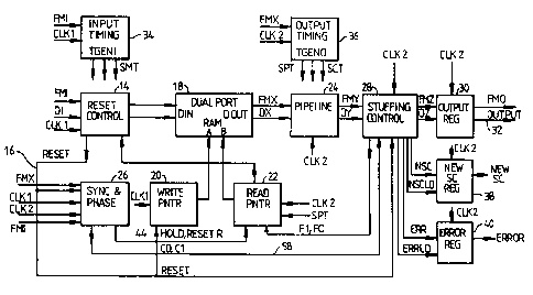
Figure 3 is a block ~iagram of one po~ible
implementation of the con~trained stuffing alqorithm
of the in~ention. In this circuit, a clock signal
CLRl is reco~ered from the incoming data stream (DI)
by known technique~. The clock signal CL~I i8
desirably at e~actly the same frequency of a locsl
clock signal CLK2 which i8 generated by an ocsillator
(not shown) at the node. In accordance with the
techniques of the invention, th~ ~tuffing algorithm
is arranged to compensate for the frequency
difference the clock signals CLRl and CLR2.
Data DI from the network i8 inputted to a
reset control circuit 14 which is clocked by the
clock CLKl. The reset control circuit 14 receives an
input ~ignal FMI which indicates the incoming frame
marker.
Figure 2A illustrate~ the incoming data
stream DI and shows the incoming frame marker FMI at
~3
~-' 't~
~. .'- ' .
~`.i ;''~...... :
~,i, ; '
~L3~27
the head of the ætuffing co~trol field 12. The
diagram also shows a stuffing management time SMT
indicator at the start of the SM field 13. ~he
diagram also shows an SPT indicator at the start of
the ~F f ield 10. The indicators 8FI, SMT a~d SPT are
all in synchronism with the clock CLRl derive~ from
the incoming data DI. Generally ~peaking, the re~et
eontrol circuit 14 generates reset 8ignal8 on output
line 16 for resetting other part~ of the circuitry,
as will be describsd herein. The data stream from the
reset control 14 pa~æes to the input of a dual port
RAM 18 which, together with write pointer 20 and read
pointer 22, funetion as an elastie buffer for
delaying ths data stream by sn amount which depends
upon the ~tuffing eontrol algorithm. The dual port
RAM 18 i~ arranged to function as a FlFO memory, for
instance of the type described in Te~as In~trument~
Data Manuals.
The delaye~ output data ~tream DX from the
dual port RAM i~ illu~tr~ted in Figure 2B. In this
diagram, the delayed frame marker is denoted as FMX.
The data stream DX i8 eoupled to the input of a
pipeline eircuit 24 which i8 eloeked by the loeal
eloek CLR2. The pipeline eireuit 2~ eomprises a
register which i8 eapable of hol~ing 5 octets of the
data stream. It funetions as a ~elay eircuit in order
for phase measurements to be made in a syne and phase
eircuit 26. Output fro~ the pipeline eireuit 24,
denoted as data stream DY, i~ eoupled to a ~tuffing
eontrol eircuit 28 whieh i8 also clockea by the local
clock CLR2. The output data stream DZ from the
circuit 28 is eonneeted to an output register 32
which again is eloeked by the loeal clock CLK2. The
output data stream on output line 32 is shown in
~ , .
~.;.;~,, ~ . ,
l.~
r
1332~2
11
Figure 2C. The output frame mar~er FM0 in this data
stream indicates the start of the stuffing control
field 12.
The circuit includes an input timing
generator 34 which is synehronised to the incoming
frame marker FMI and eloeked by CLKl. The generator
34 produces at its output the 8MT indicator which
iaentifies the octet ln the frame whieh constitutes
the SM field 13 and eontains the stuffing management
code. The stuffing management eode may inelude the
ability to reset the stuffing eontrol system for
instanc0 on system start-up.
The cireuit also inelude~ an output timing
generator 36 whieh is synehronised to tho frame
marker FMX at the out~ut of the RAM 18 nd is eloc~ed
by the loeal eloek CLX2. The generator 3C generateg
two timing signals whieh are: ~i) a ~tuffing eontrol
time 8CT to identify the 8C field 12 (whieh in the
illustrated arrangement is the same as the FMI
indieator) and (ii) a stuffing pad time ~PT whieh
identifies the first oetet of the stuffing field 10.
The eireuit ineludes a new 8C register 38
whieh holds the new value for the eode in the
stuffing eontrol field 12, generated by the ~tuffing
eontrol eircuit 28. The eireuit includes an error
register ~0 which reeei~es error ~ignal~ from the
eontrol eireuit 28. The register 40 is used as an
optional monitoring de~iee to enable monitoring of
the number of errors whieh oeeur ln the ~tuffing
eontrol which for instance may be signalled when the
~ncoming frame has too mueh stuffing or the incoming
frame has insuffieient stuffing.
I ~ 12 1~32627
Genorally ~pea~ing, the circuit funct1on
follows: the 8ync and phase cir~uit 26 measures the
phase difference between the FMI and FMX indicators.
I the mea~ured phaæe i8 equal to D, the desired
phase difference, in octet~, then no stuffing action
is required. For instanee, if the clock CLK2 is
slower than the eloek C~Kl, the measured phase will
be greater than the aesired pha~e D. In that event,
the read pointer 22, which i~ cloc~ed b~ the clock
CLK2, would tend to fall behind the write pointer 20
which is clocked by the cloc~ CLXl and this would
e~entually lead to errors. To avoid errors, ona octet
of the ~tuffing control field 10 i8 skipped by the
read pointer 22 80 as to give the read pointer 22 a
period of one octet in which to catch up. This
effectively obviateæ problems caused by differences
in frequencies between the clocks CLXl a~d CLR2. If
howe~er the incoming data stream DI has been
sub~ected to stuffing upstream, as indicated by the
content of the stuffing control field 12, further
stuffing action at the node would result in either
too much or too little stuffing, then ~o further
stuffing is possible and an error is recorded in the
register 40. If the cloc~ CL~Z i8 faster than the
clock CLKl, stuffing bits need to be added, sub~ect
to the aforementioned limits.
Thus, in the technigue of the in~ention, the
length of the ~tuffing field 10 withiD a frame
remains in selectable ~imits independently of the
number of cascaded nodes. The m~thod of control uses
not only the state of fill of the dual port ~AM 18
but also the amount of stufing already present in
the incoming data stream DI as a result of stuffing
` -
13 13.~2~2i'
actions carried out by previous nodes. A no~e is
permitted to delete to add stuffing bits in the
stuffing field SF of a frame if and only if the new
stuffing field lieæ within the selected limits. For
instance, the nominal length of the stuffing field 10
may be 16 octets ~nd it may be eon~trained to never
be less than 4 octet~ or greater than 28 octet~. At
16 octets, it is at the design level. Given the
tolerance on the clocks and the limit~ on the
stuffing field, the size of the RAM 18 can be
dimensionea 80 that overflow and underflow will not
occur for a given number of ca~caded nodes. In
operation, data i~ written into and read out of the
dual port RAM 18 and the phase difference mea~ured by
the eircuit 26 is indieative of how ~ueh information
is in the RAM 18, at any point of time. This in turn
depends on the fregueney differenee between the
clocks CLXl and CLX2.
The reset eontrol eireuit 14 produces reset
signals on output line 16 when a stuffing reset
reguest code has been written into the ~M field 13.
In addition, the reset eontrol eireuit 14 ean also
produe~ a reset signal when an internal fault i~
detected. The reset output 16 is eoupled direetly to
the reset input of the write pointer 20 and
indireetlr to the reset input of the read pointer 22
via the ~yne and phase eireuit 26.
The syne and phase eireuit 26 is illu~trated
in more detail in Figure 5. It eomprises a
synehroniser eireuit 42 whieh has FMI, CLXI, CLR2 and
reset inputs fro~ the line 16. It has an output line
44 whieh is eoupled to the reset input of the read
pointer 22. Its other output 46 i8 eonneeted to the
clear input of a phase eounter 48. The synchroniser
.
.,.~ .. . . . . . . . . , ~ . .......................... . .. . ~
'.: ~ -
-~\
1 3~2 ~
14
circuit 42 generallY speaking comprises two cascaded
flip flops which produce an output signal on line 46
which is synchronised with the FMI with respect to
CLK2. A suitable implementation for this arrangement
is described in an article entitled ~Metastable
Behaviour in Digital Systems~ by L. Xleeman an~ A.C.
Cantoni, I.E.E.E. Design and Test of Computers,
I Volume 4, 6 December, 19~7, pp 4 - 19. The phase
I counter 48 comprises an 8 bit synchronous counter
which counts clock pulses from the clock CLR2 and i~
cleared each frame by output from the synchronl~er
circuit 42 on line 50. The output of the counter
represents the running count of CLK2 pulses since the
last clearing ~ignal generated by the synchronisor
circuit ~2. The line 50 1~ connected to the input of
a phase register 52 which copies the output of the
counter into the regi~ter on receipt of an FMX ~ign~l
coupled to its load input. Thus the value in the
~- register 52 represent~ the phase difference between
FMI and FMX. The out~ut of the phase register 52 i~
coupled to a control ROM 54 which stores the value D,
the desired phase difference in octets between FMI
and FMX. The ROM 5~ produces two conditional stuffing
~: command signals Cl, C0 in accordance with the
following table:
Cl C0 Stuffing Action (Conditional)
Phase~ D L L +l
Phase~ D L N 0
Phase~ D H L -1
The stuffing command signals Cl and C0 are
conditional because the stuffing control circuit 28
.~
.1
--.
1 3 ~ 2 ~ 2 ~
may find that the incoming frame already has a code
in the stuffing control field 12 which is either at
the upper or lower limit. When the stuffing control
field is at a limit then further stuffing i8
permissable only i~ it doe~ not vialate the
constraints impose~ upon ætuffing code, as mentioned
previously. The ROM 54 coul~ of course be replaced by
comparators and logic gates in order to qenerate the
necessary command signals Cl and CO. Output from the
ROM 54 is coupled to an output register 56, the
output lina 58 of which i~ connected to an input of
ætuffing circuit 28.
The read pointer 22 i8 illustrated ~n more
detail in F~gure 4. Th~s circuit incluaes a ROM 60
~ and shift register 62. The RON 50 has hold and reset
i inputs from the 8ync and phas~ circuit 26,
unconditional ~tuffing com~and signal~ F~ and Fl from
~he stuffing control circuit 28, and the ~PT
indicator. Output from the ROM 60 (which i~ 4 b~t
parallel data) ~ 8 inputted lnto the register 62 which
i8 cloc~ed by the local clock C~R2~ The output of the
register on line 64 is coupled to the B input of the
dual port RAM 18. The output i8 also fed back to an
input o the ROM 60 via feedback line 66. The ROM 60
generates a 4 bit addre~s output and informatlon
which ensbles the reset control bloc~ 14 to check for
¦ pointer wrap-around. The read pointer 22 operates
~ synchronis~ly th~ local clock CLX2. ~he output of the
¦ read pointer i8 ~et to zero under control of the
, ' reæet block I4.
¦ The ROM 60 is arranged to produce the
following logical functions (assuminq RESET and ~OLD
I are inactive):
:
.;s, .. . .
.
;ii, - , . - - , . . ..
16 l ~ ?~ 2 ~
SPT Fl F0 New Output Efect on Stuffi~g Field
H L L old ~ 0 ~1
H L H old + 1 0
H H L old ~ 2 -1
H H H old ~ 1 0
L X X old + 1 U8ED FOR NORMAL TWO PORT READ
Note:
(a) In the abova, X means don't car~.
(~) 8PT i8 generated by output timing c$rcuit 36
to i~entify the first octet of the ~tuffing
~ield in the frame.
(c) RESET overi~es oll inputs an~ cau~e~ the
output to zoro.
(d) if RESET is i~act~ve then HOLD cau~efi the
output to remain unchanged.
(e~ Th~ ~w Output in~icat~s the read ad~r~as
for th~ read pointer.
(f) ~1 on the stuffing field lndicates an
increased length of the stuffing fi~ld 10 by
one octet an~ -1 decreases length of the
stuffing field by on~ octet.
~ he ~tuf~ng control circuit 28 i~
illu~trated ~n more dstail in Figure 6. The circuit
compris~s a ROM 68 which has inputs FMY, DY,
condition~l stuffing comman~s CO, Cl from the 6ync
ana pha~e circuit 26 and reset input from the re~et
control circuit 14. It has an output F~Z to indicate
the frame marker po~ition ~t its output, data stream
DZ after stuffing control has taken place, and
unconditional stuffing control outputs FO Fl which
ti ~
17 ~ 7~
are generated by the logic steps in the ROM 68. It
also produces the new value NSC for the ætuffing
control field 12. It produces an NSC load signal
NSCLD which is inputt~d to the load input of the
regi~ter 38. It also ha~ an error output ER~ ~n~ an
error load signal ERRLD wh~ch ig connected to the
loading input of the error register 40. The stuffing
control circuit 28 could of course be implem~nted by
us~ng logic blocks such ~8 gat~s. It i~ however most
conveniently implemente~ in the form of the ROM. The
table which ~ollows, whi~h i~ baæe~ upon a Pa~cal
language notation, 8et8 out the principal log~cal
~teps needed to generate the unconditional stuffing
command ~ignals FO and Fl, NSC and ERR signals.
..
.. i t
IF FMY~L an~ RESET-~
THEN [
DZ:.DY;
FO:DH; Fl:~H;
NSC:-O; NSCLD:.L;
ERR:-O; ERRLD:.L,
]
IF ~MY=H and RESET~
THEN t
' DZ:.s~nominal;
FO:.H; Fl:.N;
NSC:.DZ; NSCLD:.H;
ERR:=errorcodel; ERRLD:~H;
''`; '''
lR 1 3 ~2 ~2 ~
]
IF FMY=L and RESET=L
THEN [
DZ:~DY;
FO:-N; Fl:-H;
NSC:~o; N8CLD:-L;
ERR:-o; ERRLD~
IF FMYsH and RESET-L
THEN t
IF DY>SFMAX (error)
THEN t
FO:-H;Fl:-H;
NSC:-DY; NæcLD: sH;
ERR:~rrorco~e2; ERRLD:-H;
]
IF DYCSFMIN
THEN
DZ:.DY;
PO: ~H;Fl: H;
NSC:~DY; NSCLD:-H;
ERR:~errorcod~3; ERRLD:-H;
]
IF DY~SE?~AX and ~Cl eguals the complement
of CO)
~EII t
Fl:~Cl; FO:sCO;
~ ' .
~'
~:-
~,
19 1 3 ~ i- r~ ~
IF Cl~L THEN DZ:=DY ELSE DZ:.DY-I;
NSC:2DZ; NSCLD:~H;
ERR:~O; ERRLD:~H;
I~ DY~-SFMIN and ~Cl-~)
THE~ t
Fl:-CI; FO:-CO;
IF CO: ~H then DZ: ~DY ELSE DZ: ~DY~l;
NSC:-DZ; NSCLD:~H;
ERR:-O; ERRLD:.H;
~rror~ode:
errorcodel Reæet to no~inal ~tuffing ha6 occurred
errorcode2 Incoming frame has too much ~tuffing
~rrorcode~ Incoming frame has insufficient
~tuffing
Parameters
~FMAX Ma~imum allowable stuffing
~FMIN Minimum allowable stuf~ing
~FNOMINAL Nominal ~tuffing.
In accordanc~ with d secon~ a~pect of th0
invention, when th~re ar~ no e~ternally imposed
constraints, then a natural choice in framing is a
fixed number of bits per frame 6. This results in the
; ` ` . ~ . :
',' .",. ' ~ ' ,,
.''. ~ ',, ' . ~ ~' `. `
" ' ` , , , . ' '`
~ 7
most effective utilisation of transmission capacity
and least comple3 terminal equipment. Fi~ed framing
is the accepted practice wherever it is possible.
There are many instances of e~isting transmission
systems of that type. The present invention makes it
possible to use fised framing on the links, and hence
use esisting or already developed equipment where the
data transmitted has a variable frame.
A variable frame has a nominal number of
bitæ per frame with a positive and negative
variation. The frame arrangement to which the first
aspect of the invention refers is an in~tance. That
particular case ha~ a fi~ed number of data bits in
the field 8 and a variabls number of stuffinq bits in
the field 10. Another inst~nce would be wher~ the
number of data bits and the number of stuffing bit~
were both variable. (Though not described above, the
first aspect of the invention wouid be workable in
the latter case also. The only additional reguirement
then is only that there be an e~plicit indication of
the end of data as well as that of the start).
The preæent invention allows the
transmission of variable frames o~er fi~ed framed
tranæmission linkæ without imposing any delays in the
presentation of the variable framed data at the
receiving end, other than ths actual transmission
delay. It predicate~ e~plicit indications of
predictable events in the variable ramed stream to
which pointers are imbedded in the fised frame
stream. This i8 e~pl~ine~ most easily using the
specific instance of a fised length data field 8 and
followed by a variable length stuffing field 10, the
size of the stuffing field being indicated at its
I start as described previously. This is illustrated in
,.~
~' '
`\
21 3 3 ?~ ~ ~"",
Figure 2.
~ he fi~ed frame 6 will typically consist of
a time multiple~ed arrangement of frame overhead and
transmitte~ data where the frame overhead i8 used for
supervisory or management communication from
transmitter to receiver. It i8 nece~sary that there
be room in that overhRad for pointers ~ust referred
to. For the ~ake of description we as~ume that
esactly one pointer iE providsd per i~ed frame and
that it point~ to the nest predictable event (NPE)
within ths tran~mitted data. The pointer ~ould, for
instance, indicate the number of octets in the ~ata
stream following a datum in the fi~ed frame after
which the NPE will occur. It must ~150 disclose what
that particular NPE i8.
In the case of Figure 2 there are two NPE' 8 .
When the ~atum of the fised frame occur~ i~ the DATA
field of the variable fra~e, the ne~t predi~tabl~
event i8 the occurrance o~ the ~tuffing in~icator.
When the datum occurs in the ~tuffing fiald then the
NPE i8 the ~eginning of the nest DATA field, a~suming
that the ~I ha~ disclo~e~ the length of the current
stuffing field. The NPE point~r must distinguish
between these two NPE's for whi~h the pointer will
incorporate one additional bit.
A possible mechanism tha~ would generate the
pointer woule be a downward counter coupled to a
two-ætate machine. When the variable frame is in DATA
the state machine i~ in st~te '0', ~ay, and when in
the stuffing field in stat~ '1'. As it entsrs state
'0' the counter i8 set to a number equalling the
(fised) number of octets in the DATA field. With
every octet sent off on the link the counter iæ
decremented by one. Should the datum of the fiYed
,,
~4:
~'''~' '' ' ".,:"''
' : .- :
:`' . ~ ;
'.,, ~ : ' '
. : , ' ' . ~:. ' ::
';'~' , ' '~ : :
r.:, . ,,, :
- ' -. :'
'Sj --'~ :. '.
22 13^~27
frame occur while the machine is still in ~tate 'O'
the number in the counter at its occurrence will be
the pointer indicating the distance to the ne~t
stuffing indicator. As the state machine enters state
'1' the counter is ~et to the number of the stuffing
indicator and is ~i~ilarly decremented with each
stuffing octet sent off on the link. With occurrence
of datum while ~n state '1' the counter value will
again be the pointer, but not to tha start of DATA.
At the receiv~ng end interace receiYed
pointer values can be used to generate ~splicit
in~ications of the marked events. This i8
I conveniently implemented ~gain by a down-count~r. On
receipt of the pointer the counter i6 set to ths
pointer value and decremented with each octet that is
received in the data ~tream. When the count reaches
zero, the event occur~ and can be ~ignalled by the
intsrface to the eguipment that i~ connected to it.
If the DATA ~ields were vari~ble tben the
outlined technigue woul~ ~t~ll be workable provided
the DATA block~ would be prece~ed by a DATA length
indicator. On entering ~tate '0', the indic~tsd
length rather than a f~e~ number would be loa~ed
into the counter, but otherwi~e everythiDg ~ould be
as befor~. ~O
Many modifieations will be apparent~tho~e
~killed in the art without departing from the spirit
and scope of the invention.
~ , . ...
;~
: