Note: Descriptions are shown in the official language in which they were submitted.
1 334303
DIGITAL KEY TELEPHONE SYSTEM
The invention is in the field of small telephone systems and
the like, especially those sometimes referred to as key telephone
systems. More particularly, aspects of the invention relate to
digital key telephone systems, examples of which are disclosed
in a co-pending application entitled "Digital Key Telephone
System", serial number 578,754, which was filed on September 28,
1988 by George Irwin et al, and in a Canadian application
entitled "Digital Key Telephone System", serial number 581,393
which was filed on October 26, 1988 by David J. Robertson et al,
and in a Canadian application entitled "Digital Key Telephone
System" serial number 590,657 filed February 9, 1989.
The invention relates especially to a telephone system
having a central processor and a plurality of ports, each of said
ports having connected thereto an apparatus including a
processing device for controlling functions of the apparatus and
an interface device for exchanging signals in an operating signal
format of the port.
Some examples of small telephone systems have been generally
referred to as key telephone systems. Traditionally a key
telephone system is provided by extensive telephone line and
control lead wiring between key telephone sets. Each key
telephone line extends to a telephone exchange. Each of the
telephone sets includes a plurality of push button switches or
keys, each for connecting the telephone set to a particular
telephone line among a plurality of telephone lines routed to the
key telephone set. The switching function of line selection is
~^
1 334333
-
mechanically provided and distributed among the key telephone
sets. Any features in addition to plain ordinary telephone
service (POTS) must be added on a per line basis. The primary
advantage of these systems is economy with small size. However,
if such a system is required to expand along with the
organization it serves, over a time it eventually becomes more
expensive on a per line and feature basis than a private branch
exchange would be. Key telephone systems are also
characteristically of the analog signal type, and therefore are
impractical to interface with an ISDN as will likely be desired
by business customers in the near future.
Various features may be made available to the user. For
example, Automatic Call Distribution is a feature which routes
incoming external calls, on a first come, first served basis, to
the first available terminal. Such a feature finds application
in airline reservation systems, telemarketing, customer service,
and so on.
Least Cost Routing is a feature which automatically routes
outgoing calls using the least expensive route. For example,
during business hours, outgoing calls may be routed over tie
lines. After the time when lower long distance rates come into
effect, calls to the same destination may be routed over regular
central office lines. With such a feature, the user need not
worry about which line he should use, but simply dials the number
and the feature makes the decision for him.
Implementation of such a feature involves the execution by
the user's terminal of a predetermined set of functions, each of
which may comprise a number of specific steps.
1 334303
In conventional systems, software for implementing such
features is resident in the core or central processor which
serves all of the terminals. If a user requests a different set
of features, a craftsperson must access the core processor and
make the necessary changes. Likewise, if new features become
available, the craftsperson must access the core processor to
install them.
The core processor is a critical part of such a system so
any mistakes when making such alterations could have serious
repercussions.
One object of the invention is to provide for the changing
of features without necessarily accessing a central or core
processor.
Another object of the invention is to give the user more
control of the system's capabilities and permit a significant
increase in the number of features made available to users of
small telephone systems.
According to one aspect of the present invention, there is
provided a telephone system having a central processor and a
plurality of ports, each of said ports having connected thereto
an apparatus including a processing device for controlling
functions of the apparatus and an interface device for exchanging
signals in an operating signal format of the port, at least one
of said apparatus being a telephone station apparatus and another
of said apparatus being a feature host apparatus, said telephone
station apparatus having a plurality of functions stored therein
and said feature host apparatus having a plurality of feature
modules stored therein, each such feature module comprising
D
1 334303
instructions for controlling an exchange of signalling and
supervision messages between said feature host apparatus and said
telephone station apparatus so as to invoke a predetermined group
of said functions in said telephone station apparatus and provide
thereby a selected one of said features in response to a feature
request action of a user at said telephone station apparatus.
Each feature module may be accessible by means of a unique
logical address, the telephone station apparatus having storage
means for storing such logical addresses and accessing them in
response to the feature request action of a user. Conveniently,
the storage means may associate each such address with a user-
selectable code generated by such feature request action. The
telephone station apparatus may include translator means for
detecting such a user-selectable code and transmitting the
corresponding logical address to said feature host apparatus.
Each such function may comprise a set of steps to be
executed in performing the function, and the telephone station
apparatus further comprise means for performing the steps in
response to selection of the corresponding function by the
feature host apparatus.
The system may comprise storage means for the functions and
function selector means operable in response to the feature host
to access the storage means and selectively invoke said
functions.
The telephone station apparatus may comprise a session
manager operative to exchange messages with the feature host
apparatus to establish communication therebetween before the
feature host apparatus assumes control of the functions of the
....
1 334303
telephone station apparatus and, thereafter, to exchange messages
with the feature host apparatus to terminate such communication.
Where the system includes function selector means, a message
handler may be provided to detect whether a message from the
feature host is destined for the session manager or the function
selector means and route such message accordingly. In either
case, the session manager may respond to the feature action
request to establish said communication.
According to a second aspect of the invention, there is
provided is a method of utilizing a feature apparatus in a
telephone system having a central processor and a plurality of
ports, each of the ports being available for connection of an
apparatus thereto, each such apparatus including a processing
device for controlling functions of the apparatus, and an
interface device for exchanging signals in an operating signal
format of the port. The method comprises the steps of:
a) providing a plurality of said apparatus being connected
at a corresponding plurality of said ports, at least one of said
apparatus being a telephone station apparatus and another of the
apparatus being said feature apparatus;
b) providing at least one time multiplexed message channel
in association with each of the ports;
c) routinely selecting one of said apparatus for
transmission of a signalling and or supervision message via its
port associated message channel; and
d) in response to a feature request action of a user at
said telephone station apparatus, exchanging signalling and
supervision messages between said telephone station apparatus,
B
` 1 3343~3
said feature apparatus and said central processor whereby said
feature is provided by said feature apparatus on behalf of said
telephone station apparatus.
According to another aspect of the invention, there is
provided telephone station apparatus for use in a telephone
system having a central processor and a plurality of ports; each
of said ports having connected thereto an apparatus including a
processing device for controlling functions of the apparatus and
an interface device for exchanging signals in an operating signal
format of the port; at least one of said apparatus comprising a
feature host apparatus having a plurality of feature modules
stored therein, each such feature module comprising instructions
for controlling an exchange of signalling and supervision
messages between said feature host apparatus and said telephone
station apparatus so as to invoke a predetermined group of
functions in said telephone station apparatus and provide thereby
a selected one of said features in response to a feature request
action of a user at said telephone station apparatus. Said
telephone station apparatus comprises storage means for storing
a plurality of said functions, and function selector means
operable to invoke said stored functions selectively in response
to said signals from said feature host.
According to a further aspect of the invention, there is
provided feature host apparatus for use in a telephone system
having a central processor and a plurality of ports, each of said
ports having connected thereto an apparatus including a
processing device for controlling functions of the apparatus and
an interface device for exchanging signals in an operating signal
q:
1 334303
format of the port; at least one of said apparatus being a
telephone station apparatus having a plurality of functions and
function selector means for selectively invoking a predetermined
group of said functions thereby to provide a selected one of said
features in response to a feature request action of a user at
said telephone station apparatus. Said feature host apparatus
comprises a plurality of feature modules stored therein, each
such feature module comprising instructions for controlling an
exchange of signalling and supervision messages between said
feature host apparatus and said telephone station apparatus.
According to yet another aspect of the invention, there is
provided a feature module for use in a telephone system having
a central processor and a plurality of ports, each of said ports
having connected thereto an apparatus including a processing
device for controlling functions of the apparatus and an
interface device for exchanging signals in an operating signal
format of the port, at least one of said apparatus being a
telephone station apparatus having a plurality of functions and
function selector means for selectively invoking a predetermined
group of said functions thereby to provide a selected one of said
features in response to a feature request action of a user at
said telephone station apparatus, and another of said apparatus
being a feature host apparatus having a plurality of feature
modules stored therein, each such feature module comprising
instructions for controlling an exchange of signalling and
supervision messages between said feature host apparatus and said
telephone station apparatus and a unique logical address; and
said feature host apparatus comprises means for detecting such
~1
~ 1 334303
a logical address in an incoming message and routing said message
to the corresponding one of said feature modules, said feature
module comprising address codes for a unique set of said
functions and sequence control means for controlling
implementation of said set of functions, by said telephone
station apparatus, in such a sequence as to provide the
corresponding feature.
In this specification the term "logical address" means a
unique address which is assigned to a particular terminal (or
feature) and does not change when the terminal is relocated.
Preferably the logical address is associated with the user, for
~ . ~
~.~
.c.
1 334303
example a prime directory number. The term physical "address",
however, is used for an address which is unique to each port.
Hence when a terminal is relocated, it has a new physical
address. Its primary use is to facilitate the establishing of
a communications channel within the system.
Embodiments of the invention will now be described, by way
of example only, with reference to the accompanying drawings, in
which:
Figure 1 is a block diagram of a key telephone system in
accordance with the invention;
Figure 2 is a block diagram of a software architecture for
supporting FUNCTIONAL station or terminal apparatus in the key
telephone system in Figure 1;
Figure 3 is a block diagram of a software architecture
similar to the software architecture illustrated in Figure 2, but
with an added capability of supporting STIMULUS station apparatus
as well as the FUNCTIONAL station apparatus;
Figure 4 is a graphical illustration of operating timing
pulses and or signals generated within a circuit switch module
used in Figure 1;
Figure 5 is a block diagram of a timing sequence generator
used in the circuit switch module for providing the timing
signals illustrated in Figure 4;
Figure 6 is a block schematic diagram of counters, used in
a circuit switch module in Figure 1, and arranged to provide time
slot and channel addresses for operation of the circuit switch
module;
1 334303
Figure 7 is a block schematic diagram of a converter circuit
used in the circuit switch module in Figure 1;
Figure 8 is a graphical illustration of timing signals used
in the operation of the converter circuit in Figure 7;
5Figure 9 is a block schematic diagram of a time switch
circuit used in the circuit switch module in Figure 1 to provide
circuit switched communication paths in the key telephone system;
Figure 10 is a block schematic diagram of a time switch
conference circuit in the circuit switch module and used in
10combination with the time switch circuit of Figure 9 to provide
a conference feature in the key telephone system;
Figure 11 is a block schematic diagram of an interface
circuit used in the key telephone system of in Figure 1;
Figure 12 is a block schematic diagram of a processor
15interface circuit used in the key telephone system illustrated
in Figure 1;
Figure 13 corresponds to Figure 3 but is an alternative way
of representing the software architecture;
Figure 14 illustrates the terminal apparatus in more detail;
20Figure 15 is a state machine diagram illustrating frame
recovery which is used to initiate the initialization sequence;
Figure 16 illustrates, in more detail, a database manager
of the central processing unit and related components of the
system;
25Figure 17 illustrates message flow between a functional
terminal and the database manager;
l O
1 334303
Figure 18 illustrates message flow between a stimulus
terminal apparatus, functional terminal emulator and the database
manager;
Figure 19 illustrates the manipulation of the stored data
following relocation or replacement;
Figure 20 is a data flow diagram representing the data flow
in the data base manager;
Figure 21 is a data flow diagram illustrating data flow in
a functional terminal;
10Figure 22 is a data flow diagram illustrating data flow in
a functional terminal emulator;
Figure 23 is a detail diagram illustrating registers in the
TCM interface of a terminal apparatus;
Figure 24 is a detail diagram illustrating registers in the
15central processor interface;
Figure 25 is a diagram, corresponding to Figure 2, showing
a feature host apparatus and a functional terminal controllable
thereby, both connected to the system S and S channel;
Figure 26 is a data flow diagram illustrating data flow in
20those parts of the functional terminal of Figure 25 which are
involved in feature implementation;
Figure 27 illustrates the sequence of messages exchanged by
the functional terminal and the feature host apparatus in setting
up a session providing a particular feature requested by a user;
25Figure 28 illustrates state changes in the functional
terminal and the feature host during the session illustrated by
Figure 27, and;
1 3343~3
Figures 29 and 30 illustrate other optional states for the
functional terminal.
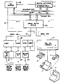
In Figure 1 a digital key telephone system provides for
connection of various digital telephone instruments, as
exemplified at 13 and 14, and various digital data terminals,
personal computers or the like, as exemplified at 15 and 17,
which are able to communicate, via the system, with one another
as appropriate, and with other devices via line or trunk circuits
23. The lines and or trunks serve to connect the digital key
telephone system with other telephone facilities, for example a
central office or private exchange (not shown). A back bone of
the digital key telephone system is provided by a short parallel
time division multiplex (TDM) bus 10, which provides a wide band
communication path between up to nine 64 channel circuit switch
modules 100, a central processor interface circuit 8 and tone
sources 26. If any of the tone sources 26 provide an analog
signal, such is coupled into the system via a lead 27. The bus
10 is referred to as a primary bus, and a secondary bus 20,
similar to the primary bus 10, provides for unidirectional
communications from the interface circuit 8. Each of the circuit
switch modules 100 couples 64 ten bit transmit serial channels
to predetermined corresponding time slots in the bus 10, and up
to 64 parallel selected TDM time slots on either of the buses 10
or 20 to 64 ten bit receive serial channels. Thirtytwo of the
serial transmit and receive channels are coupled to an internal
ports circuit 12 via a serial TDM path 11. The remaining
thirtytwo serial transmit and receive channels are coupled to
external port circuits at 22 via a serial TDM path 21.
B
1 334303
Each of the channels is capable of transmitting a binary
signal pulse stream at a rate of 80 kilo bits per second, with
at least 64 kilo bits per second being available as a channel for
pulse code modulated (PCM) voice information, or data
information. The remaining sixteen kilobits may be committed to
supervisory and signalling communications, in association with
the PCM or data information. In this example the internal ports
circuit 12 consists of sixteen TDM time compression multiplex
(TCM) interfaces. The TCM method of signal transmission is
sometimes referred to as "Ping Pong" transmission. Each of these
interfaces provides a transmit path between each of TCM links 19
and two predetermined and fixed serial TDM channels in the serial
TDM path 11. In a similar manner analog signals are interfaced
to and from various circuits shown at 23, 24 and 25, via the
serial TDM path 21 and the external ports 22 provided by CODEC
circuits. Alternatively, it may be advantageous to provide an
external TDM port for interfacing with another telephone facility
via a digital signal transmission link, T1 or DS30 for example.
However, in this case, each CODEC circuit interfaces with a
predetermined and fixed transmit and receive channel pair of the
serial TDM path 21. Hence, for each and every port (that is a
place where a digital telephone instrument or other digital
device or a digitally interfaced or compatible line, trunk and
the like may be connected to the digital key telephone system),
there is at least one predetermined ten bit parallel time slot
in the primary bus 10 which is allocated to receive information
from such device, line or trunk. In an alternative example, the
time slots on the bus 10 correspond to such device, line or trunk
~3
B
1 3343~3
for the purpose of transmitting information thereto. However,
such alternative example is not herein further discussed.
A central processor 7 is coupled via the interface circuit
8 to the primary bus-10 for communication via a predetermined
thirtytwo of the ten bit parallel time slots. The interface
circuit 8 may receive all ten bits of each time slot on the bus
10. Normally, only the two bits corresponding to a sixteen
kilobit sub-channel are transferred from the bus 10 to the
central processor 7 by the interface circuit 8, for purposes of
call control. The interface circuit 8 provides signalling and
supervision from the central processor 7 via the secondary bus
20 at time slot occurrences corresponding to intended line
appearance destinations via the appropriate circuit switch module
100. Therefore each circuit switch module 100 transmits 10 bits
to the primary bus 10 but receives and switches only 8 bits from
the primary bus 10. The other two bits are received at the
appropriate time via the secondary bus 20.
In this example, each port associated communication path
provides for full duplex operation with two words, of ten bits
each, being exchanged every 125 micro seconds. In at least one
of these words, bit positions 0-7 are dedicated to one of data
or voice, the bit position 8 is dedicated to signalling and
supervision, and the bit position 9 is dedicated to validation
of signalling and supervision. The signalling and supervision
information is collected from, and distributed to, the port
associated channels via the interface circuit 8 under the
direction of the central processor 7. The collected information
is gathered into byte groupings by the interface circuit 8 for
1~ ^
B
_ 1 334303
transfer to the central processor 7 and by a somewhat
complementary function, information is distributed from the
central processor 7, via the interface circuit 8 into bit
position 8 of a selected one of the channels or of all the
channels.
The key telephone system is intended to support two
generically different types of station apparatus: one being a
very basic telephone station set hereafter referred to as a
STIMULUS set or an S set, which includes a bit stream interface
device, a simple processing device, and a CODEC; and the other
being a more complex featured autonomous station apparatus which
may take the form of a proprietary key telephone set, interface
apparatus, or proprietary display telephone or data terminal.
Such instrument is referred to as a FUNCTIONAL set and such
reference is intended to indicate that the apparatus contains
some call processing instructions in the form of software or
firmware. For convenience, any station apparatus which is not
an S set is hereafter referred to as a FUNCTIONAL set or an F
set.
In the S set, any change in its operating state, for example
ON HOOK to OFF HOOK or a key depression, is communicated to the
central processor 7 via the S set processing device, the bit
position 8 and the interface device. This is accomplished in the
S set by a continuous (request to send RTS) assertion of "00 in
the bit position 8 and 9 of the outgoing channel, until a
validated clear to send (CTS) is received in bit positions 8 and
9 of the incoming channel. When the CTS is recognized in the S
set a STIMULUS protocol message indicating OFF HOOK is
1~
B
1 334303
-
transmitted via the S and S bit positions 8. Thereafter, a
typical call progress proceeds by way of exchange of STIMULUS
protocol messages.
By way of exemplary contrast in the F set, a request to send
(RTS) may be generated after an OFF HOOK is followed by
sufficient telephone call dialling information having been keyed
in by a telephone user. In this case the processing device and
its operational programming perform basic call processing and,
in addition to providing dial tone at the appropriate moment, may
also generate ring back or busy tone. The F set communicates in
a similar manner to the S set, using the S and S bit positions
8. After a CTS is received from the central processor the F set
transmits a FUNCTIONAL protocol message.
Table 1 illustrates structural arrangements of messages of
STIMULUS protocol and FUNCTIONAL protocol in the KSU-to-terminal
direction.
TABLE 1
__ ________________
HEADER TYPE LENGTH
Binarv (HEX)
0X000000(40H)
to STIMULUS 1 BYTE
OX011111(5FH)
OX100000(60H)
to STIMULUS 2 BYTES
OX100111(67H)
OX101000(68H)
to STIMULUS MULTI-BYTE
OX101111(6FH)
OX110000(70H)
to FUNCTIONAL VARIABLE
OX111111(7FH)
1~
B
~ 33~43~3
In the header, bit positions left to right are 7 through 0.
In particular, bit positions 5 and 4 indicate the protocol of the
message. FUNCTIONAL messages in this arrangement are indicated
by both of the bit positions 5 and 4 being asserted 1 .
STIMULUS MESSAGES are indicated by at least one of the bit
positions 5 and 4 being asserted "0 . The purpose of each of the
bit positions in the header is illustrated in Table 2.
TABLE 2
BIT 7 6 5 4 3 2 1 0
PURPOSE START CLEAR PROTOCOL SECONDARY
TO INFORMATION
SEND
In the case of a header being in a range of 40H - 5FH, the
header is the actual message, the gist of which is carried in the
bit positions 3-0. In messages of more than one byte, the second
and subsequent bytes carry information. The quantity or number
of the information bytes within a message are specified in lesser
significant bit positions of the header.
The CTS bit position indicates a clear to send message and
is only of significance when received by an F set or an S set.
Table 3 illustrates the structural arrangements of messages
of stimulus and functional protocol in the terminal-to-KSU
direction. In this direction, bit 7 is a start bit with value
1, as shown in Table 4.
` I 334303
TABLE 3
_______________________________________________________________
Header Type Length
Binary (Hex)
_______________________________________________________________
1000 0000 (80H) Stimulus 1 byte
to
1101 1111 (DFH)
10 ------------------------------------___________________________
1110 0000 (EOH) Stimulus 2 bytes
to
1110 0111 (E7H)
_______________________________________________________________
1110 0000 (EOH) Stimulus multibyte
to
1110 1111 (EFH)
_______________________________________________________________
1111 0000 (FOH) Functional variable
to
1111 1111 (FFH)
______________________________________________________________
TABLE 4
BIT 7 6 5 4 3 2 1 0
PURPOSE start protocol secondary information
There is no CTS bit in this direction, since the KSU 40
does not wait for acknowledgement from the terminal when
transmitting a message to it. Message flow control is only for
signalling messages sent from the terminal to the KSU 40.
Plural protocols and central processor flow control of
messages, communicated via the S and S bit positions, permit
advantageous software architectures as illustrated in Figures 2
and 3, to be resident in a key telephone system as shown in
Figure 1. In Figure 2, a key system unit (KSU) 40 includes
common equipment 41 coupled with an S and S channel 50 via
software elements, namely a network controller 42 and a data base
/g
B
1 334303
-
manager 43. The common equipment 41 is in effect representative
of a hardware interface with the buses 10 and 20 in Figure 1 but
also includes firmware and software resident in the central
processor 7. In this example, the central processor 7 is
provided by a 68008 microprocessor available from Motorola Corp.,
of 1303 East Algonquin Road, Roselle, Illinois, 60196, U.S.A.
The central processor 7 is arranged to support modularized
software elements such as the elements 42 and 43.
The S and S channel is a message channel which is in
operational effect common to all the FUNCTION station apparatus
of the system. Exemplified are F sets 51 and 52, an automatic
call distribution (ACD) terminal 53, a system management data
retrieval (SMDR) terminal 54 and an outboard trunk unit 55 for
connection to a central office (not shown). Each of these is
a FUNCTIONAL apparatus which includes its own processing device
and call processing software.
Figure 3 illustrates an example of an architecture
configured similarly to Figure 2, but for supporting STIMULUS
sets in addition to FUNCTIONAL sets. In this case, the common
equipment 41 also supports additional modular software in the
form of FUNCTIONAL emulators 45, 46 and 47. These FUNCTIONAL
emulators perform, on behalf of respective STIMULUS sets 61 and
62, and a STIMULUS trunk unit 63, to make these appear to the
rest of the key telephone system to also be FUNCTIONAL sets.
Hence, in some system configurations, economy on a per port basis
is achieved. It should be noted that FUNCTIONAL elements 52-54
may also be present in Figure 3 but were omitted for convenience
of illustration.
I7
B
1 334303
-
In operation of the key telephone systems in accordance with
Figure 2 or 3, any F set receiving a CTS message is able to
transmit to all FUNCTIONAL entities, be these apparatus or
emulators. Likewise, F emulators are able to transmit to all
FUNCTIONAL entities but as the F emulators are software based in
the KSU 40, the previously discussed arbitration ritual of RTS
and CTS is not required. Any FUNCTIONAL entity which may thus
respond or act in accordance with its own programming as
warranted by the content of the transmitted FUNCTIONAL message.
Any such FUNCTIONAL message involving a STIMULUS set is
intercepted and subsequently acted upon by the corresponding
FUNCTIONAL emulator software module. This effectively results
in a series of STIMULUS messages being exchanged between the
FUNCTIONAL emulator and its associated STIMULUS set via its S and
S channel. For example, S set 61 and emulator 45 exchange
messages via an S and S channel 61a.
In FUNCTIONAL messaging the message bits are distributed or
relayed to every channel occurrence in each frame. Although
STIMULUS sets or units are thus exposed to the FUNCTIONAL
messages, the STIMULUS processor devices therein are arranged to
disregard FUNCTIONAL messages as recognized by the distinct
header as illustrated in the foregoing tables 1 and 2. On the
other hand, STIMULUS messages are unidirectional. Distribution
of a STIMULUS message is confined to the channel occurrence which
corresponds to a STIMULUS set for which the STIMULUS message is
destined.
Flow control of FUNCTIONAL and STIMULUS messages is
discussed from a hardware viewpoint after the following
,~0
B
; 33A303
discussion of the structure and operation of the modular circuit
switch module 100 with reference to Figures 4-10.
In order that each of one or more circuit switch modules 100
be able to transfer information from the serial TDM paths 11 and
21 to the parallel TDM bus 10 without contention, a phased timing
sequencer, as shown in Figure 5, resides within each of the
modules 100 for regulating the functions of the module. Wave
forms exemplified in Figure 4 illustrate a master frame timing
pulse occurring at a rate of 1 Khz, clock pulses numbered 0-27
occurring at a rate of 5.12 MHz and state machine timing pulses
SM0-SM10. With the switch module 100 installed in the system,
a preset start decoder 101 is connected to a hard wired location,
not shown, which provides an identity, that is a fixed four bit
binary word, ID0-ID3. The combination of the signal states of
the bits ID0-ID3 is unique for each possible switch module
location in the digital key telephone system. The preset start
decoder 101 generates a 5 bit binary word on a bus 102, in
response to the combination of bit states as shown in table 1.
A five bit counter 103 is preset by each occurrence of the master
frame pulse, to correspond to the word on the bus 102 and
thereafter is incremented with each occurrence of a clock pulse.
An output 104 of the counter 103 is decoded by a decoder 105
which generates a reset signal on a lead 106 with each occurrence
of a count of 19 in the counter 103. Thus with the occurrence
of the next clock pulse, the counter 103 is reset to a count of
zero. Thus a modulo 20 counting function is provided, which is
phased as is illustrated in table 5.
~1
B
TABLE 5 l 334303
CIRCUIT ID3 ID2 ID1 IDO PRESET TDM-11 TDM-21
5 SWITCH VALUE OF FRAME AND FRAME AND
MODULE BUS 102 TIME SLOT TIME SLOT
CORRESPONDENCE CORRESPONDENCE
O O O O 0 18 0 2
1 0 0 0 1 17 1 3
2 0 0 1 0 14 4 6
3 0 0 1 1 13 5 7
4 0 1 0 0 10 8 10
0 1 0 1 9 9 11
6 0 1 1 0 6 12 14
7 0 1 1 1 5 13 15
8 1 0 0 0 2 16 18
In accordance with the table, for example for the circuit
switch module 0, the channel zero on the serial TDM path 11 is
inserted onto the parallel TDM bus 10 in time slot zero, channel
one in time slot 20 and so on until the last channel, channel 31,
of a serial TDM frame is inserted into time slot 620.
Stated in other terms, each TDM path has 32 parallel ten bit
receiving channels assigned to it on the primary bus 10, and each
of these channels is separated from the other by 19 other channel
occurrences.
The decoder 105 also generates an SM0 timing pulse,
coincident with the count of 19 occurring in the counter 103.
A shift register 109 responds to the SM0 timing pulse and the
a2
1 33~3~
-
clock pulses to generate additional timing pulses SM1-SM10 as
illustrated in Figure 4.
Referring to Figure 6, the time slot occurrences on the
parallel TDM bus 10 are tracked by a parallel slot counter which
5includes a modulo 20 counter 111 and a modulo 32 counter 112.
The counter 111 responds to the 5.12 MHz clock pulses to provide
repetitive counts of 0 through 19 on five time slot count leads
TSC 0-4. The counter 112 is incremented with each reset
occurrence in the counter 111 to provide repetitive counts of 0
10through 31 on five time block count leads TBC 0-4, whereby in
combination binary signals on the TSC and TBC leads define 640
parallel time slot addresses per frame. A serial channel counter
function is provided by a counter 113 which provides 32 channel
counter addresses on serial channel count leads SCC 0-4 to define
15channel occurrences in the serial TDM paths 11 and 21. The
counter 113 is incremented with each time block occurrence as
indicated by the timing pulse SM6. All of the counters 111, 112
and 113 are reset with each occurrence of the master frame pulse.
The converter circuit illustrated in Figure 7 resides within
20the circuit switch module 100 and performs both serial to
parallel conversions and parallel to serial conversions for each
of the 64 TDMT and the 64 TDMR channels on the TDM paths 11 and
21. As before mentioned, the TDMT channels are incoming and
carry data or voice, plus signalling bits originating at the
25terminal instruments, while the corresponding TDMR channels are
outgoing, each to the originating terminal instrument. Each
incoming time slot includes 10 binary bits which are converted
directly to parallel form and asserted during the predetermined
a3
B
1 334303
time slot interval on the primary bus 10. Each outgoing time
slot includes 10 binary bits which are obtained from one of two
sources: one source being a corresponding time slot interval on
the secondary bus 20; the other source being 8 bits from any time
slot interval on the primary bus 10, the 8 bits having traversed
the time switch, plus 2 bits from the time slot interval on the
secondary bus 20 corresponding to the TDMR channel occurrence.
The converter circuit is discussed in more detail with
reference to the timing signals illustrated in Figure 8. A SYSTEM
CLOCK waveform shown at the top of Figure 8, and some of the
other waveforms in Figure 8, are idealistically depicted for
convenience as having vertical rise and fall portions. Actually,
in practice these waveforms have sloped rise and fall portions
similar to those waveforms illustrated in Figure 4, which are
more realistically depicted. The converter circuit, in Figure
7, includes three orthogonal shift registers shown at 501, 502
and 503 respectively. These three registers perform the required
serial to parallel, and parallel to serial conversions. Each of
the orthogonal shift registers 501, 502 and 503 is associated
with a clock generator, not shown, which produces non-overlapping
timing signals, illustrated in Figure 8, for shifting and
directional control. Vertical directional control signals V1,
V2 and V3 are used to vertically direct shift functions of the
register 502, 501 and 503 respectively. Horizontal directional
control signals H1, H2 and H3 are used to horizontally direct
shift functions of the registers 502, 501 and 503. The actual
loading of D type flip flop elements in the registers 502, 501
and 503 is clocked by signal pulses S1, S2 and S3. The control
.f~
` 1 334303
signals V2 and V3 are shown in broken line to indicate that these
signal pulses are 20 system clock periods removed from the
adjacent H2 and H3 signal pulses, such that each commences at 40
system clock intervals.Bits of the TDMR serial bit streams are
timed to be coincident with the rising edges of a serial digital
loop clock signal C690. Bits of the TDMT serial bit streams on
the paths 11 and 21 are sampled and re-timed to likewise be co-
incident, by latches 511 and 521. A half cycle of the system
clock prior to the rising edge of the serial digital loop clock
signal C690, contents of the (2 by 8) outgoing register 502 are
selected by a receive multiplexer 535 to provide the first bits
of each of the TDMR channels at 11 and 21. The receive
multiplexer selection is in response to a MUX SEL OUTGOING
control signal shown in Figure 6. The outgoing bits are timed
by the rising edge of the clock signal C690 to start transmission
of a 10 bit time slot. Shortly thereafter, the starting bits of
the corresponding TDMT channels are sampled by the latches 511
and 521 using the falling edge of the same clock signal C690.
The sampled bits are then applied (2 by 2) to the incoming
register 501. During the said same clock signal C690, contents
of the register 502 and the incoming register 501 are asserted
in parallel by a multiplexer 532 on the leads of the primary bus
10. Only in an instance of a time slot (TS) 19 occurrence, which
is indicated by a rising edge of a decode 18, in Figure 6, will
the multiplexer 532 gate Z bus signal states to the P bus 10.
A half cycle of the same system clock signal after the falling
edge of the said same C690 clock signal, the three orthogonal
registers 501, 502 and 503 are clocked, resulting in the incoming
2 ~
1 334303
register 501 accepting said starting bits, the outgoing register
503 moving the second outgoing bit to the multiplexer 535, an~
the register 502 moving 8 bits of the TDMT path 21 toward the
multiplexer 532. At the same time the incoming register 501
moves the remaining two bits toward the multiplexer 532 via a
multiplexer 533. The next two outgoing parallel information
bytes are moved through data holding registers 504 and 505, under
control of timing signals SM2 and SM6 and hence, into the
register 502. At the same moment, as before described, the
regis'er 501 stores the first two bits of each incoming TDMT
channel. Once the first two bits have occurred, the registers
501 and 503 receive no further clock signals until the start of
the next outgoing time slot sequence when all 10 registered bits
are shifted in parallel toward the P bus 10.
At the start of the next time slot sequence, registers 501
and 503 are caused to move their respective contents (2 bits)
vertically, that is upwardly in Figure 5. Thereafter the next
eight TDMT bits are shifted vertically into the register 502 and
the previous contents are likewise shifted out to be transmitted
via the multiplexer 535 and the TDMR paths 11 and 21. The
horizontal directional control signals and the vertical
directional control signals continue to be alternately asserted
thereby repeating the parallel to the serial and serial to
parallel cycle for each TDM channel on TDM paths 11 and 21.
The time switch circuit in Figure 9 provides for a timely
transfer of 8 information bits from one of the 640 time slots on
the primary bus 10 to a parallel T bus input of the parallel
input multiplexer 506 of the converter circuit in Figure 7, and
1 334303
thereby ultimately to a TDM path (11 or 21) time slot, as
directed by the central processor 7. The information bits of
each time slot on the P bus 10 are momentarily captured by a data
input latch circuit 710 and thereafter applied at an input 702
of a dual port random access memory (RAM) 701. The dual port RAM
701 includes an output 703 which drives a T bus 770 in response
to a six bit address applied at a read access address port 704.
The RAM 701 differs from a typical dual port memory device in
that for the purpose of storing information received at its input
702, it does not include the typical address decode circuitry.
Instead, each write address is decoded and applied to an
individual one of 64 write enable leads at 706. The decoded
write address is timed via a write enable latch and strobe
circuit 720. Any number of the write enable leads may be
asserted by the circuit 720 simultaneously. The dual port RAM
701 responds, to a signal assertion or signal assertions on any
or all of its 64 write enable leads at 706, by storing the signal
states of said 8 information bits at the corresponding memory
location or locations as the case may be. For example, if none
of the leads at 706 is asserted, no storage locations are
written. If one or more of the leads at 706 is asserted, the one
or more corresponding storage locations are written. Reading of
the 64 dual port RAM storage location occurs sequentially on a
regular and periodic basis, under the control of a flip flop, not
shown, in the latch 711 which is toggled by signals SM2 and SM6,
and the 32 sequentially generated TDM channel addresses which are
generated by the counter 113 in Figure 6.
2~
,,i~ .
1 334303
A connection memory 730 contains information as to the actual
time slots of the 640 P bus 10 time slots from whence information
bit states are stored in the dual port RAM 701. The connection
memory 730 is provided by a content addressable memory which
includes an eleven bit data input port 731, a six bit address
port 732 and a 10 bit compare address port 733. The general
structure and operation of contènt addressable memories is known.
In this example P bus addresses, from whence information is to
be stored, are lodged in memory locations in the connection
memory 730. Each of 64 memory locations, not shown, correspond
with a separate one of 64 output leads at 736. A digital
comparator, not shown, is associated with each of the 64 memory
locations such that addresses appearing at the compare port 733
are each compared with the information stored at each of the 64
memory locations. In every instant where the address at the
compare port 733 and the information at a memory location is the
same and the memory location also includes an asserted validity
bit, the corresponding one of the 64 output leads at 736 is
asserted. The asserted state is eventually transferred via the
circuit 720 to the dual port RAM 701, which responds as
previously described.
Operation of the circuit switch modules 100 is directed by
the central processor 7, which uses the interface circuit 8 and
32 dedicated time slots on the P bus 10 for lodging information
into the memory locations of the connection memory 730 via a data
latch circuit 740 and an address latch circuit 750. The
information is delivered from the interface circuit 8 in the form
of four bytes each of which occupies time slot 19 of 4
~g
B
1 334303
sequentially occurring time blocks on the P bus 10. The four
bytes include a command byte, followed by an address byte, a low
order data byte, and a higher order data byte. Each of these
bytes is asserted along with a validity signal on one of the two
remaining leads of the P bus 10 which indicates that the bytes
are in fact an instruction from the central processor 7. A
portion of the command byte specifies either a write or a read
function intended for one of a connection memory, a source
connection memory or a destination connection memory. A
comparator responds to the validity signal and a match between
a remaining portion of the command byte and the ID0-3 by causing
the address latch to store the next byte, that is the address
byte. Thereafter the data latch 740, in Figure 9, captures 11
bit states of the low and higher order bytes, which are
subsequently stored in the memory location of the connection
memory 730 as indicated by six address bits asserted by the
address latch 750. Provision is also made for the central
processor 7 to confirm the information content of any address in
the connection memory. In this case the command byte indicates
the read function, and the address byte indicates the memory
location to be read. The subsequent low and higher order bytes
are driven by the stored information from a data output 738 of
the connection memory 730 and via an output latch 712 and buffer
713 to the Z bus and thence via the multiplexer 532 in Figure 7
onto the P bus 10 where it is picked up by the interface circuit
8.
The time switch conference circuit in Figure 10 provides a
three party conference feature in the digital key telephone
c27
1 334303
system. The time switch conference circuit adds an ability for
a timely transfer of 8 information bits from another of the 640
time slots on the P bus 10, ultimately to, for example, said TDM
path time slot previously referred to at the beginning of the
discussion of Figure 9. Very briefly by way of introduction,
bytes are presented to a multiplexer 992, in Figure 10, via the
T buses 770 output from Figure 9 and via a conference C bus 991.
The four most significant bit (not including the sign bits) of
each byte are compared in a comparator 993 which directs the
multiplexer 992 to assert the 8 bits from the C bus 991 on the
T bus 540 in the event that the value of the 4 bits from the C
bus 991 is equal or greater than a value of the 4 bits from the
T bus 995. In the event the T bus 995 value is greater, then the
8 bits from the T bus 995 are asserted on the T bus 540 by the
multiplexer 992. Thus a three party conference call may be
implemented wherein each party hears only the instant loudest
speaking party of the other two parties.
Considering the time switch conference circuit of Figure 10
in more detail, the information bits of each time slot on the P
bus 10 are momentarily captured by a PCM input latch 910 and
thereafter applied at an input 902 of a dual port RAM 901. The
dual port RAM 901 includes an output 903 which is buffered to the
C bus 991 via a PCM output latch circuit 990. Likewise the T bus
770 is buffered to the T bus 995 via a latch circuit 994. The
dual port RAM 901 differs from the dual port RAM 701 in that it
has only 16 memory locations and lacks typical address decode
circuitry for the purpose of reading out information stored at
these memory locations. Each write address is decoded and
3o
`t~
1 334303
applied to an individual one of 16 write enable leads at 906 and
likewise each read address is decoded and applied at an
individual one of 16 read enable leads at 907. The decoded write
address is timed via a write enable latch and strobe circuit 920.
Likewise the decoded read address is timed via a read enable
latch and strobe circuit 970. The read enable latch and strobe
circuit 970 also includes an EXCLUSIVE OR logic circuit not
shown, which responds to a single decoded read address occurrence
by asserting a compare enable signal on a lead 971. The compare
enable signal is used to activate the selection function of the
comparator circuit 993, which in the absence of the compare
enable signal causes the multiplexer 992 to assert the T bus g95
bit states onto the T bus 540, exclusively. Hence if no decoded
read address or more than one decoded read address is asserted
at inputs of the read enable latch and strobe circuit 970, the
conference function does not occur. The dual port RAM 901
responds, to a signal assertion on a write enable lead at 906,
by storing the signal states of said 8 information bits at the
corresponding memory location. Likewise, reading of a memory
location in the dual port RAM 901 occurs in response to a
corresponding read enable lead at 907 being asserted.
A source connection memory 930 contains information as to the
actual P bus time slots from whence information bit states are
stored in the dual port RAM 901. The source connection memory
930 is provided by a content addressable memory having 16 memory
locations, not shown, each corresponding to a separate one of 16
output leads at 936. The source connection memory 930 includes
an eleven bit data port 931, a six bit address port 932 and a ten
31
g,~
1 334303
bit compare address port 933. A digital comparator, not shown,
is associated with each of the 16 memory locations such that
addresses appearing at the compare port 933 are each compared
with the information stored at each of the 16 memory locations.
In an instant where the address at the compare port 933 and the
information at a memory location are the same and the memory
location also includes an asserted validity bit, the
corresponding one of the 16 output leads at 936 is asserted. The
asserted state represents a decoded write address, which is
subsequently transferred via the circuit 920 to the dual port RAM
901 which responds as previously described.
A destination connection memory 980 contains information as
to the actual TDMR time slots on the TDM paths 11 and 21 to which
information bit states stored in the dual port RAM 901 may be
directed via the multiplexer 992 and the T bus 540. The
destination connection memory 980 is of a structure similar to
that of the previously described source connection memory 930.
Addresses appearing at a compare port 983 are each compared with
information stored at each of 16 memory locations. In an instant
where the information at the compare port 983 and the information
at a memory location are the same and the memory location also
includes an asserted validity bit, a corresponding one of 16
output leads at 986 is asserted. The EXCLUSIVE OR logic circuit
in the read enable latch and strobe circuit 970 permits the
corresponding read enable lead at 907 to be asserted, which
causes the dual port RAM 901 to read out the 8 information bit
states from the corresponding memory location as previously
described.
3~
`_ I 334303
The information appearing at the compare port 983 is asserted
from the channel counter bus leads SSC 0-4 by a channel counter
latch circuit 911. The latch circuit 911 also includes a flip
flop, not shown, which is toggled by the timing signals SM2 and
SM6 and thereby provides 64 addresses per frame, similar to that
previously discussed in relation to the latch circuit 711.
Operation of the conference function in the digital key
telephone system is directed by the central processor 7, which
uses the interface circuit 8 to communicate with the 32 dedicated
time slots on the P bus 10 for lodging information into the
memory locations of the source connection memory 930 and the
destination connection memory 980 via a data latch circuit 940
and an address latch 950 in a manner similar to that previously
discussed in relation to the connection memory 730. Likewise the
central processor 7 may confirm the information content of the
source connection memory 930 by way of a data output 938, a data
output latch circuit 912, a buffer circuit 913 and the Z bus,
connected as shown in Figure 8. Information content of the
destination connection memory is also available to the central
processor 7 by way of a data output 988, a data output latch
circuit 914, a buffer circuit 915, and the Z bus, connected as
shown in Figure 10.
A primary function of the interface circuit 8, as illustrated
in Figures 11 and 12, is that of receiving S and S messages and
distributing S and S messages. The S and S messages are received
from the primary bus 10 in one port related time slot at any one
time by S and S receive buffer registers 810. The S and S
messages are transmitted to all of the secondary bus 20 time
7 3
1 334303
slots or to a selected one of the secondary bus 20 time slots by
S and S transmit buffer registers 820. The S and S messages are
physically coupled with the primary and secondary buses 10 and
20 by a bus buffer circuit 801. The interface circuit is
similarly coupled to central processor address and data buses,
at 898 and 899, by a processor buffer 805. A primary function
of the buffers 801 and 805 is that of relaying signals between
all of various potential signal sources and destinations while
minimizing the actual number of receiving gates and driving gates
physically attached to the buses and various unillustrated timing
and control leads. Provision of such buffers is usual in digital
electronic systems and does not warrant detailed discussion.
Another primary function of the interface circuit 8 is that
of capturing requests to send (RTS) an S and S message. As
before described, an RTS occurrence is marked by 'zero'
occurrences in bit positions 8 and 9 in a time slot. A valid
signal detector receives each bit 9 time slot state and detects
and latches the 'one' state for a short time. A request to send
detector 816 likewise receives each bit 8 time slot state. If
the valid signal detector 815 is unlatched and the bit 8 state
is 'zero', the RTS detector 816 asserts a request to send signal
indication on an RTS lead 816a. If the request to send is from
within a selected group of time slots, a receive shift clock
(RSCL) causes a shift register portion of the buffer registers
810 to shift the RTS indication into the buffer register 818.
After sixteen RSCL pulses, a receive load clock (RLCL) causes the
contents of an intermediate two byte shift register to be
transferred to a two byte output register. The contents of the
3 ~
, ~
1 334303
output byte register are available at the processor buffer 805
via an S and S message bus 812. Thus the registers 818 are
clocked to monitor a group of 16 specified ports in the key
telephone system for RTS occurrences. An occurrence of an RTS
during any input from any of the 16 specified ports is arranged
to generate a low level interrupt to alert the central processor
to the presence of information. However, as it is intended that
each port connected apparatus will continuously RTS until a clear
to send (CTS) is received by it, there is no particular urgency
attached to any one RTS occurrence. Eventually, the central
processor will specify transmittal of an appropriate CTS and
simultaneously select the port related time slot as a source of
an expected S and S message.
When a CTS message is detected in the intended station
apparatus a response, in the form of at least a one byte message,
is transmitted. The first bit of the message is a 'one' in the
bit 8 position and a valid 'one' in the bit 9 position. This
combination causes a start bit detector 817 to raise a start bit
(SB) signal for the duration of subsequent uninterrupted valid
signal detection occurrences, coincident with the selected time
slot. In the presence of the SB signal, RSCL pulses (one per
frame) cause bit 8 states of the selected time slots to be
shifted into the S and S receive buffer registers 810. Interrupt
signals are generated with every byte so collected, such that the
central processor is able to receive and if necessary, internally
queue the incoming S and S message.
Outgoing S and S messages are received from the processor
buffer 805 via a bus 822 as timed by transmit load (TL) pulses.
~ 3
3~ .
1 334303
A shift register in the register 820 shifts received bytes, bit
by bit toward the bus buffer 801 at a rate of one bit per frame
in response to transmit shift clock (TSCL) pulses. The state of
the output stage of the shift register is continuously applied
to a transmission gate 823. For this operation, the transmission
gate 823, and an idle bit driver 828, are both responsive to a
time slot select (TSS) signal. In the case of a stimulus
message, this TSS signal is derived from a transmit port
register 2480 (Figure 24) which is written into by the central
processor 7 in dependence upon the destination port number. In
the case of an F message, the TSS is asserted throughout the
length of the message continuously, frame after frame. In the
case of an S message, the TSS is asserted for the duration of the
time slot associated with the destination port of the S message.
The idle bit driver asserts a 'one' on the lead 829 when the TSS
is not asserted. A valid signal driver 825 responds to the TSS
assertion by asserting a 'one' on a lead 826, whereby S and S bit
assertion on the lead 829 are accompanied by valid signal bit
assertion on the lead 826.
Another capability of the interface circuit 8 is that of
providing wide band data paths between any of the port associated
64 Kb/s channels and the central processor 7. Input is received
from any specified channel via a data receive buffer 830 under
the control of a read bus (RB) strobe, which is generated
coincident with occurrence of a primary bus time slot from which
receiving is required. This occurrence preferably raises a high
level interrupt which is intended to result in a write to
processor (WP) strobe being generated to provide the buffered
~ t 3G
~ 334303
byte on a bus 831 for use by the central processor 7. In like
manner, bytes of information are transferred from the central
processor 7, via a data transmit buffer 840 to a bus 841, for
assertion during a predetermined time slot on the primary bus 10.
Although the buffers 830 and 840 provide a convenient data
transport interface, this type of interface can be unduly time
consuming if such transfers are to occur frequently. For
example, frequent data transfers are required between the switch
modules 100 and the central processor 7, in order to exercise
prompt control of communication paths in the key telephone
system. Hence, a more specialized interface is provided which
operates throughout the 32 time slots on the primary bus 10,
which are dedicated to exclusive use by the central processor 7,
as previously described. Connection instruction bytes are
loaded from a bus 863 to a four byte FIF0 861 via a multiplexer
860 in the presence of a write (W) signal. After the FIF0 861
has received four bytes, the central processor 7 must direct the
interface circuit to initiate transfer of data to the circuit
switch 100 via a bus 866 and the primary bus 10. The interface
circuit asserts the bits states appearing at the FIF0 output onto
the primary bus 10 with each occurrence of a dedicated control
time slot. If no information transfer is required, an idle code
is asserted on the bus 863 and therefore is subsequently asserted
on the bus 866. By this means, up to 32 bytes of connection
instruction can be transferred via the primary bus during each
frame. Up to 16 bytes of query and 16 bytes of response
information may be exchanged via the primary bus 10 by loading
the FIF0 with a 2 byte query message.
3 7
b~
1 3343Q3
-
Functional circuit blocks in Figure 12 interface with the
central processor 7 via the same processor buffer 805, shown in
Figure 11. In Figure 12, a time slot address generator 880
similar to that discussed in relation to Figure 5 provides
definition of time slot interval occurrences on the primary and
secondary buses for the interface circuit 8. Particularly,
address registers 881 are selectively loaded via the buffer 805
from the central processor 7 to define; those time slots which
are watched for RTS, that time slot which is granted S and S
message transmission to S and S receive buffer registers 810; and
the time slot selected for single channel transmission of an S
and S STIMULUS message or a CTS message.
In operation, a comparator apparatus 882 monitors the
contents of the address registers 881 and the time slot address
occurrences from the generator 880. Occurrences of matches, in
combination with instruction of central processor origin and
signals from the detectors 815-817, are used to generate the
controlling signals in sequence and with timing as previously
discussed in relation to Figure 11. A status and interrupt
circuit 883, monitors the progress of S and S message transfer,
data byte transfers, and control byte transfers, with reference
to signals of detector and control origin, to generate timely
interrupt signals whereby the central processor is informed of
information exchange opportunities and requirements.
The common equipment 41 shown in Figures 2 and 3 will
include, among other things, a message repeater software module
to relay messages between terminals. As illustrated in Figure
13, in which components corresponding to Figures 1, 2 and 3 have
~?g
_ 1 334303
the same reference numerals, a message repeater 1601 comprises
a functional message repeater 1601A and a stimulus message agent
1601B. Functional terminals 51 and the outboard trunk unit 55
are shown connected to functional message repeater 1601A by TCM
channels 19. Likewise functional emulators 45, 46 and 47,
respectively, are shown connected to functional message repeater
1601A by way of the S and S channel 50 and to the stimulus
message agent 1601B by stimulus S and S channels 61a, 62a and
63a, respectively. Two stimulus sets and a stimulus trunk unit
61, 62 and 63, respectively, are shown connected to the stimulus
message agent 1601B by respective TCM links 19. The functional
message repeater 1601A receives functional messages from
functional terminals or the database manager 43 or the network
control 42 and broadcasts them to all functional entities in the
system.
The previously discussed difference between functional
message headers in the two directions implies that a functional
message received by the KSU 40 central processor 7 must be
modified before being broadcast in the opposite direction to
other terminals. This function is performed in the KSU 40
central processor 7 by a message repeater 1601 (see Figure 13),to
be discussed later. The stimulus message agent, however, is
capable of only point-to-point communications with the stimulus
terminals 61, 62 or stimulus trunk unit 63, or with the
corresponding functional emulators 45, 46, 47.
Each of the terminals 13, 14, 15, 17 provides an interface
between a user and a TCM communication channel. In telephony,
this communication channel typically terminates in analog
3 ~
1 334303
transducers for voice communication, although this is not
necessarily the case. User actions requiring interaction with
the KSU 40 are detected and result in transmission and reception
of messaging on the signalling and supervision channel provided
by the system.
Referring to Figure 14, at the hardware level there may be
minimal difference between stimulus and functional terminals, at
least so far as signalling to the central processor 7 is
concerned. The distinction is confined to the terminal processor
1488. For a functional terminal, the processor 1488 is
programmed to respond to and generate functional messages on the
signalling and supervision channel 50. In a stimulus terminal,
the processor sends and receives only stimulus messages, ignoring
any incoming functional messages which may be present on the
channel. It should be noted that these two message types are
distinguished by their unique header formats. (See Table 1)
The block diagram of Figure 14 represents either a functional
terminal or a stimulus terminal. A large portion of the
functionality of the terminal is provided in a single hardware
component, the Digital Terminal Interface Chip (DTIC) 1470. The
functional blocks within the DTIC 1470 include a TCM interface
1475, D channel interface 1476, speech envelope detector 1478 and
codec 1480, linked by two separate buses 1471 and 1472,
respectively. Bus 1471 is a parallel bus that accesses data
registers via a processor interface 1473. These registers are
resident in each of the functional blocks, and allow a processor
off the chip to control and obtain status specific to that
functional block. The second bus, 1472, is a synchronous serial
~0
` 1 334303
bus carrying signalling and supervision channels and
communication channel data in a format similar to TCM.
A terminal hardware identifier 1474 comprises an Erasable
Programmable Read Only Memory (EPROM) to store a digital
identifier that is unique in the system. In this example, the
identifier 1474 is a 40 bit code that may be written to the
device once only after completion of manufacture.
This identifier 1474 may be read by the terminal processor
1488 via a terminal processor interface 1473.
The signalling and supervision channel and the communication
channel are combined and put into a Time Compression Multiplexed
digital format. The TCM interface 1475 performs the multiplexing
and demultiplexing of these channels for transmission to and
reception from the TDM TCM interface 12 in the KSU 40, by way of
an analog interface circuit 1495 which provides amplification and
buffering. TCM interface 1475 detects absence of the TCM signal
transmitted from the KSU 40 and records this status in a status
register 2300 (Figure 23) readable via the processor interface
1473. This allows the terminal processor 1488 to detect
connection of the terminal to the KSU 40.
The signalling and supervision channel is known as the D
channel portion of the TCM frame. The D channel interface 1476
receives both stimulus and functional messages originating from
the KSU 40 and formats them for the processor interface 1473.
Messages originating from the processor 1488, to be transmitted
to the KSU 40, are formatted for the TCM frame. In addition, D
channel flow control protocol (clear to send CTS/request to send
41
i 334303
RTS - see later) is handled by D channel interface 1476 as
discussed previously.
A speech envelope detector 1478 is provided as part of local
voice signal processing used in performing a handsfree function
in the terminal. Also, a combined analog to digital encoder and
digital to analog decoder (codec) 1480 is included to provide
voice communication.
Various analog inputs 1482 are provided for voice
communication, such as a handsfree microphone, handset microphone
or headset microphone. Various analog outputs 1484 such as for
a loudspeaker, handset transmitter or headset transmitter, are
also provided. Amplification and level control of these analog
signals is provided, as well as switching of the analog inputs
and output between these various transducers by an analog
interface 1486. In addition, audible user indications such as
tones and a ringing signal are generated by the analog interface
1486.
User input to the terminal is detected as key depressions
that close switches in the key matrix 1490 and result in input
signals to the processor 1488. The technique for detecting these
key depressions is widely used in many types of electronic
keyboards. The processor 1488 reads the key matrix rows at
regular time intervals for these inputs, while simultaneously
generating an output signal sequentially on each of the matrix
columns.
Visual indication to the user is provided by liquld crystal
display (LCD) indicators driven by LCD drivers 1492. The state
B
1 334~03
of these indicators is controlled by the processor 1488 in
response to user actions and incoming messages.
A liquid crystal display module 1494 provides visual
representation of text to the user of the terminal. Characters
are written to this module by the processor 1488 using a common
8 bit code such as ASCII. Text may be contained in incoming
messages, or may be generated locally by the terminal processor
1488. In this example, the display module 1494 can display two
lines of 16 characters.
10The terminal processor 1488 is a general purpose
microprocessor. For both stimulus and functional terminal
apparatus, the software executed by the processor 1488 i$
responsible for decoding and encoding incoming and outgoing
messages, respectively, on the signalling and supervision channel
1550, responding to hardware inputs 1473, 1490, 1494. generated in
the terminal, and driving hardware outputs 1473, 1492, 1494.
For a stimulus terminal 61 the processor 1488 is a Mitsubishi
50743 single chip microcomputer, with software contained in Read
Only Memory (ROM). This software encodes user events and
terminal status into outgoing stimulus messages, and decode$
incoming stimulus messages to drive the user indicators. It also
provides local control of terminal hardware.
For a functional terminal, the processor 1488 typically has
more processing power, and a larger address space. Since the
software must provide functionality equivalent to that of the
functional emulator 45 in the KSU 40, a processor such as the
Motorola 68008 used in the KSU 40 is suitable, with separate
hardware devices for memory and input and output. Thus a
~3
1 334303
functional terminal 51 has a higher hardware cost than a stimulus
terminal 61 of equivalent user interface functionality.
Figure 21 illustrates data flow within the functional
terminal 51's software, which comprises both data and processing
components.
External inputs are functional messages received by way of
the signalling and supervision channel 50, and local inputs from
terminal hardware 1473, 1490 and 1494, respectively. Hardware
inputs include transducers to detect user actions, and registers
to provide access to the status of hardware subsystems in the
terminal.
Outputs are directed to hardware outputs 2132 and S and S
channel 58. Hardware outputs 2132 give audible and visual
indications to the user via terminal hardware 1473, 1492 and
1494, and provide control of hardware subsystems in the terminal
via terminal components 1473 and 1494. Operational data in table
1611 maintains a record of interactions between the terminal and
other functional entities in the system. This data is updated
in response to functional messages sent to and received by the
terminal.
Administration data in table 1612 records the settings of
terminal specific parameters that control the behaviour of the
terminal. The terminal also includes local copies in table 1612
of system and terminal specific administration data maintained
by the database manager.
Incoming functional messages are received by the terminal
over the signalling and supervision channel 50. These messages
provide information regarding the activity of other functional
.
; ^~
t J
~ 334303
entities in the system. Outgoing functional messagss are
generated by the terminal in response to local hardware inputs
and received functional messages. These messages provide
interaction with other functional entities in the system. The
processing components of the functional terminal are partitioned
to deal with the two specific types of inputs: hardware and
functional messages.
The hardware input handler 2135 updates internal data and
generates both messaging and hardware outputs. It responds to
local user inputs, and status changes detected in hardware
subsystems.
Figure 22 illustrates data flow within the functional
terminal emulator software. Each functional terminal emulator
45 has a functional message handler 2220 and a stimulus message
handler 2222. The functional message handler 2220 updates
internal data and generates both functional and stimulus
messaging. It responds to functional messages received from the
signalling and supervision channel 50.
To a large extent, the data flow within the functional
emulator 45 is identical to that of the functional terminal 51.
The key distinction is that direct hardware inputs 2131 and
outputs 2132 are replaced by incoming and outgoing stimulus
messages, 2225 and 2226 respectively, on the signalling and
supervision channel 61a.
With the exception of stimulus messages replacing hardware
data, the functional emulator data components are substantially
identical to those of the functional terminal 51. Since multiple
functional emulators are implemented on a single shared processor
1 334303
in the KSU 40, the organization of operational and administration
data components of the functional emulator 45 differs from their
organization in the functional terminal 51. This organization
within the KSU 40 was illustrated in Figure l9B.
Incoming stimulus messages are originated by the physical
stimulus terminal 61, and indicate user action or terminal
status. There is a one to one correspondence between a
functional emulator 45 and a physical terminal 61, and the
stimulus messages 2225 from a stimulus terminal 51 are handled
exclusively by one functional emulator 45.
Outgoing stimulus messages 2226 are generated by the
functional emulator 45 to update audible and visible user
indicators at the physical stimulus terminal 61. The functional
emulator 45 generates stimulus outputs 2226 for one stimulus
terminal 61 exclusively.
The hardware input handler of the functional terminal is
replaced by a processing component, stimulus message handler
2222, to handle incoming stimulus messages 2225 in the functional
emulator 45. The functional message handler 2220 is
substantially identical in both the functional terminal 51 and
functional emulator 45.
The stimulus message handler 2222 updates internal data and
generates both functional and stimulus messaging. It responds to
user inputs and stimulus terminal status, reported in incoming
stimulus messages 2225.
At the software level, signalling and supervision message
flow differs for functional and stimulus messages even though
both message types share a common physical channel at the
4~
B
- i 334303
hardware level. This distinction is possible at the software
level due to the distinct headers of the two message types. At
the hardware level message flow is identical for both stimulus
and functional messages.
At the hardware level, messages are transmitted from, say
terminal 13 to the central processor 7 (Figure 1). Within the
terminal 13 are the hardware components shown in Figure 14
including the processor 1488 which writes a message into its
memory, for example in response to a user action such as a key
depression detected in the key matrix 1490. The processor 1488
copies this message one byte at a time into a "transmit data"
register 2301 in the D channel interface 1476 via the processor
interface 1473 (see Figure 23).
Following RTS and CTS flow control handshaking with the KSU
40, the TCM interface 1475 inserts the message bits into the TCM
frame on the TCM loop 1496. Once the D channel interface 1476
is ready to accept the next byte of the message, the DTIC 1470
signals the terminal processor 1488 with an interrupt. The
processor 1488 then writes the next byte of the message into the
"transmit data" register 2301 in the D channel interface 1476.
Terminal 13's TCM loop is time division multiplexed with
other TCM loops by the TDM TCM interface 12 in the KSU 40. The
message then passes via the serial TDM link 11 and the circuit
switch module 100 onto the primary bus 10, where the S and S
channel bits are collected by the interface circuit 8. Once a
byte of the message is assembled, processor 7 reads the message
byte from a "receive data" register 2478 (Figure 24) in the
interface circuit 8. In addition, the port number of the
1 334303
terminal originating the message is read by the processor 7 from
the "receive port" register 2479 in the interface circuit 8. In
response to subsequent interrupts from the interface circuit 8,
the processor 7 buffers subsequent received bytes from the
"receive data" register 2478 in memory until the entire message
is received. Software in the processor 7 then examines the
message and takes appropriate action. The data registers 2478
and 2481 will correspond to registers 810 and 820, respectively,
in Figure 11. The port registers 2479 and 2480, respectively,
will be connected in a similar manner.
For message transmission from the KSU 40 to, say the terminal
13, the reverse process is followed. Software in the central
processor 7 writes an outgoing message into a block of memory.
Before transmission of the message begins, a "transmit port"
register 2480 (Figure 24) in the interface circuit 8 is written
by the message repeater 1601 specifying the port on which the
message is to be sent. The message may be sent on one port only,
or on all ports simultaneously (broadcast). The message is
written one byte at a time by the message repeater 1601 (Figure
16) to a "transmit data" register 2481 in the interface circuit
8. The interface circuit 8 writes message bits to the secondary
bus 20 with the appropriate timing. When it is ready for the
next byte of the message, the interface circuit 8 interrupts the
central processor 7. The central processor 7 responds to this
interrupt by writing the next byte of the message to the
"transmit data" register 2481 in the interface circuit 8. The
message bits appear at the TCM loop 19 connected to the
destination terminal 13 after passing from the secondary bus 20
. .
~,
1 334303
-
to the circuit switch module 100, and via the serial TDM link 11
and the TDM TCM interface 12.
Within the terminal 13 shown in Figure 14, the message bits
are passed through the TCM interface 1475 and collected via the
D channel interface 1476 after a "start" bit is recognised in
interface 1476. Once a complete byte of a message is assembled,
the DTIC 1470 interrupts the terminal processor interface 1473.
The processor 1488 reads the message byte from the "receive data"
register 2302 (Figure 23) in the DTIC 1470. The processor 1488
reads subsequent message bytes from the "receive data" register
2302 in response to subsequent interrupts from the DTIC 1470.
Software in the terminal processor 1488 then examines the message
and takes appropriate action.
Stimulus messages are buffered separately from functional
messages in memory in the KSU 40 central processor 7. For
messages received from terminals, the message repeater 1601
examines the header byte of the incoming message and selects the
buffer. For outgoing messages, the software generating the
message chooses the appropriate buffer based on the message type.
For both incoming and outgoing messages, the source and
destination port numbers are included in the buffer.
Stimulus message flow at the software level is exemplifed in
the sequence of initialization messages in Figure 18.
When a stimulus terminal is transmitting to the KSU 40, a
pointer to a received stimulus message is passed to a single
functional emulator 45 via a procedure call, providing access to
the S and S channel 61a by the functional emulator 45, in the
~ . ~
1 334303
terminal-to-KSU direction. This message is processed by the
stimulus message handler 2222 (Figure 22).
For signals transmitted from KSU 40 to a stimulus terminal,
outgoing stimulus messages are generated by the functional
emulator 45 by internal processing components stimulus message
handler 2222 and functional message handler 2220 (Figure 22).
These messages are placed in the appropriate buffer memory in the
KSU 40 central processor 7, after which they are transmitted to
a single TCM port.
Examples of functional message flow at the software level are
illustrated in Figures 17 and 18.
Within the KSU 40 processor 7, software passes a pointer to
a received functional message via a procedure call to functional
entities such as 42, 43, 45, 46 and 47 within the KSU 40
software, to provide a virtual S and S channel 50 within the KSU
40. Each functional message is passed to each functional entity
in the KSU 40, in order to provide the equivalent of broadcasting
on the physical S and S channel external to the KSU 40. Within
the functional emulator 45,the functional message handler 2220
processes the incoming message.
Outgoing functional messages, generated by functional
entities such as 42, 43, 45, 46 and 47 within the KSU 40, are
placed in the appropriate buffer memory in the KSU 40 processor
7, after which they are passed both to functional entities
internal to the KSU 40, and also broadcast to all TCM ports.
External to the KSU 40, the functional message handler 2134
in the functional terminal software in Figure 21 processes an
incoming functional message that has been written into a memory
S
_ 1 334303
buffer by the functional terminal processor 1488 in Figure 14.
The functional terminal software also writes outgoing functional
messages to a memory buffer in the terminal processor 1488
(Figure 14) that are sent to the KSU 40 via the DTIC 1470.
Figure 16 illustrates the system components involved in
implementing terminal relocation or replacement and shows
multiple terminal devices 51, 52 and a functional emulator 45
which communicate with each other and with database manager 43
via the message repeater 1601. The message repeater has multiple
physical connection points or ports 1602 - 1606 and the S and S
channel is accessible at each of these ports. Only functional
messaging is relevant to Figure 16.
Each of the message ports 1602-1606 is an interface point
between the associated terminal and the rest of the system and
is bidirectional, i.e. messages may be both sent and received by
a connected terminal. Messages may be addressed specifically to
other terminal apparatus in the system, or may contain no
explicit destination address. The address of the originating
terminal is included in the message. The relationship between
address and port number is not fixed, i.e. a terminal address is
unchanged when a terminal is moved to a different port.
As mentioned previously, the message repeater 1601 is part
of the KSU 40, and is mainly resident in the interface 8 with
some processing capability in processor 7. It includes a
functional message repeater 1601 (Figure 16) ~hich receives
messages sent by individual terminal apparatus and broadcasts the
messages to every signalling channel, providing the common S and
S channel 50 between functional terminals. The message repeater
~/
1 334303
1601 can identify the port of the originating terminal uniquely,
and adds this originating port number to the address information
in the message. The message, with the originating port number
included, is then broadcast by the message repeater 1601 to all
terminal apparatus in the system.
The database manager 43 is a KSU resident functional entity
that communicates with other functional entities in the system
via the signalling and supervision channel 50. In effect, the
database manager 43 is a special terminal that is permanently
attached to the system, and is not relocatable. Thus this
database manager terminal 43 need not contain a unique
identifier. It will be appreciated, however, that only one
database manager 43 may be present in the system. Like other
terminal apparatus, the database manager 43 has message
transmission and reception capabilities, in this case by means
of message handler 1607 which is a processing component of the
functional entity.
The database manager 43 maintains a Port Map Data table
1608 which stores, for each terminal, port number, identifier
(HWid) and address or prime directory number (PDN) in a
predetermined relationship. The PDN is used as a key to other
terminal-specific data resident in the database manager 43, and
is the number by which a terminal is identified to the user. The
PDN is analogous to the telephone number of a telephone set in
the public telephone network. Alternatively the other terminal
specific data may be referenced directly by HWid, or some other
unique address, rather than PDN. In addition to the "Port Map
Data" table 1608, the database manager 43 comprises "Terminal-
~æ
.~S
,~`L.,J
_ 1 33430~
specific Administrative Data" table 1609, and "Other Data" table1610.
The "Port Map Data" table 1608 contains an entry for each
terminal port in the system, and the port number is used to index
the table. Each entry contains two fields: the hardware
identifier idl---idn of the terminal most recently attached to
the port, and the corresponding Prime Directory Number PDNl to
PDNn of this terminal. This "Port Map Data" table 1608 is
updated in response to "Query PDN" messages received by the
message handler 1607 of the database manager 43.
In "Administration Data" table 1609, the database manager
43 maintains administrative data specific to individual terminal
apparatus indexed according to the PDNs of the terminal
apparatus. This data includes such information as system
controlled feature assignments that are not writable by the
individual terminal apparatus.
In addition to terminal specific administration data, in
table 1609, the database manager 43 maintains other
administration data, that applies system wide, in table 1610.
On each attachment of the terminal to a port in the system,
or each system initialization, the terminal goes through a
process of internal initialization, which involves writing data
to initial states, and initializing states of terminal hardware.
Thus, its internal processor 1488 sets variables, carries out
checks, tests, etc. turns off indicators, sets hardware ports
to known states. When internal initialization has been
completed, it is ready for external initialization, following
which it can begin communicating with other functional entities.
S3
B
1 334303
Figure 15 is a state diagram illustrating the way in which
initial connection of the terminal is deemed to have taken place
by virtue of the fact that frame synchronization has been
established following initial physical connection or reconnection
following a disruption which effectively constitutes
disconnection. Framing information is transferred to DTIC chip
1470 (Figure 14) as bipolar violations embedded at a rate of
1kHz. in the BPRZ-AMl (Bipolar Return to Zero-Alternate Mark
Inversion) signal received over the TCM loop 1496. Such a
bipolar violation is inserted in the start position of every
eighth frame or burst of the TCM signal. The bipolar violation
is timed relative to the stop bit of the preceding burst. The
frame state machine (Figure 15) enters the out-of-frame mode
(state 2) whenever it misses two consecutive violations, and upon
power-up or reset. It has recovered frame when, after a bipolar
violation (state 3), a second violation is detected exactly eight
bursts later. When a violation occurs at the wrong time during
inframe mode (mode 1), it is ignored. No TCM bursts are
transmitted in out-of-frame mode. It should be noted that the
transition from state 2 to state 3 requires only a bipolar
violation, whereas the transitions from, respectively, state 3
to state 0 and from state 1 to state 0 require both a bipolar
violation and the occurrence of a stop bit in the proper
location. In order to avoid bipolar violations between
successive transmit and receive bursts, the start bit of the
transmitted burst of the DTIC chip 1470 is given the opposite
polarity to that of the previously received stop bit. This has
the affect of changing the polarities of start and stop bits at
~ ",. q
,.~
`_ 1 334303
the 1kHz rate. Frame information is transferred to and from the
rest of the system through the serial bus 1472. (Figure 5)
As indicated in Figure 15, when the frame state machine is
in the inframe mode, a '1' is present in the status register 2300
in TCM interface 1475. Whenever an out-of-frame condition
exists, a '0' is present in the status register 2300.
The processor 1488 polls the status register 2300 at regular
intervals. When it detects a transition from '0' to '1', it
presumes that a terminal has been newly-connected and transmits
the identifier signal to the central processor 7.
If the status register indicates that the terminal has been
connected, the terminal signals its presence to the central
processor 7, by sending a message to the database manager 43.
As previously mentioned, the message handler 1607 is the
processing component of the database manager 43. It receives
incoming messages and generates outgoing functional messages via
the signalling and supervision channel 50 (Figure 2). It
accesses the data components of tables 1608, 1609 and 1610 in
response to incoming read and write request functional messages.
Although, at this stage, the functional terminal 51 is
unaware of its own PDN, it knows the fixed address of the
database manager 43, and so can address its message properly.
For a functional terminal 51, the external initialization
message sequence consists of two messages as illustrated in
Figure 17. The first message Query PDN (port,HWid,type)' is
originated by the functional terminal 51 and sent to the database
manager 43.
3~
~s
1 334303
-
This first message queries the PDN of the functional terminal
51. The hardware identifier (HWid) of the functional terminal
51, which is unique in the system, and the port number on which
the message originated, are included as parameters in this
message. The type" parameter is included by the originating
terminal to allow the database manager 43 to make terminal type
d-istinction in the terminal specific data table 1609 (Figure 16).
As mentioned previously, the originating port number is
written into the message by the message repeater 1601 (Figure 16)
in the KSU 40 rather than by the originating functional terminal
51, and is included when the message is broadcast on the
signalling and supervision channel 50 (Figure 2). Thereafter the
functional terminal 51 will ignore all incoming functional
messages except the response from the database manager 43.
This response comprises the second message, PDN response
(port, HWid, PDN,type)' whereby the database manager 43 informs
the requesting functional terminal 51 of its PDN. The PDN (prime
directory number) assigned to the terminal by the database
manager 43 is included in the message. Since the terminal 51
receiving the message does not yet know its PDN, it needs some
other means of recognizing that this message is addressed to it.
For this reason, the hardware identifier (HWid) is included in
the response message. The functional terminal 51 matches the
hardware identifier (HWid) in the message with its own in order
to recognize itself as the destination. The functional terminal
51 then saves the PDN and port number parameters received in
the message in its operational data (1611) in the terminal
processor 1488. (For the purpose of this description, the
B
~ 334303
operational data tables in both functional terminals and
emulators are deemed to be the same and so have the same
reference numeral, 1611.) The terminal 51 may then ask the
database manager 43 for other terminal specific data. In these
subsequent queries, the terminal 51 uses its own address (PDN),
rather than its identifier HWid, since the PDN is only 16 bits
long compared to 40 bits for the identifier. Thus the HWid is
only used during initialization. Thereafter messaging uses the
PDN for terminal identification purposes.
10Since the port number also is unique within the system, it
is included in the PDN response message.
Figure 18 illustrates the corresponding message sequence for
initialization of a stimulus terminal 61, which communicates with
the database manager 43 by way of a functional terminal emulator
1545. (see also Figures 3 and 13). The combination of functional
terminal emulator 45 and stimulus terminal 61 is equivalent to
the functional terminal 51 in Figure 14.
One difference between the functional terminal emulator 45
and a functional terminal 51 is that the functional emulator 45
is aware of its port number before any messaging occurs. This
allows initialization of terminal types that do not have unique
hardware identifiers, since the functional emulator 45 can
recognize itself as the destination of the 'PDN Response message
from the database manager 43 by matching the port number.
Relocation of these terminal apparatus without unique hardware
identifiers is not supported. The PDN of these terminal types
is fixed in relation to the port.
1~
..,-
1 334303
Functional messaging between the functional terminal emulator45 and the database manager 43 as shown in Figure 18 is identical
to that shown in Figure 17 between a functional terminal 51 and
the database manager 43 for functional terminal initialization.
However, a stimulus message sequence occurs between the physical
stimulus terminal 61 and the functional terminal emulator 45
before the emulator 45 generates the "Query PDN(port,HWid,type)"
functional message.
Once it has completed its internal initialization, (see
above) the stimulus terminal 61 indicates its presence to the
functional terminal emulator 45 by generating a "Reset
Acknowledge" message. This is the first indication to the
emulator 45 that a stimulus terminal has been connected
physically to the port.
The functional terminal emulator 45 requires information
regarding the characteristics of the attached stimulus terminal
61 which may affect its operation, both during and after
initialization. For example, the stimulus message meaning may
vary between terminal types, in which case the emulator 45 needs
to know. Consequently, the functional terminal emulator 45
responds with a "Query characteristics" message.
The stimulus terminal 61 responds to the query from the
emulator 45 with a "response(characteristics)" message containing
the requested characteristics. If the characteristics in this
response identify the stimulus terminal 61 as a type of device
having a unique hardware identifier, the emulator 45 transmits
a "Query HWid" stimulus message to the stimulus terminal 61. If
the stimulus terminal 61 is of a type which has no unique
Sg
1 3343~3
-
identifier, no query is made and the emulator 45 proceeds
directly to exchange functional messages with the database
manager 43, using a nil value for the hardware identifier.
Otherwise the functional terminal emulator 45 will not commence
the functional message interaction with the database manager 43
until the stimulus terminal 61 has responded to the "Query HWid"
message from the functional emulator 45 with a message "response
(HWid)" containing the requested identifier. Thereafter the
functional message interaction between the emulator 45 and the
database manager 43 takes place as previously described.
Referring now to Figure 19, initialization will usually
result in updates to the port map data (Figure 16 and 19A) in the
database manager 43. If the terminal is a stimulus device 61 with
a functional terminal emulator 45, emulator data may also be
updated (Figure 19B).
In addition to data tables 1608, in the database manager 43,
the KSU 40 has "Operational Data" and "Administration Data"
tables 1611 and 1612, respectively, each row of the tables
accessible by one of the functional emulators 45. The port map
data table 1608 is updated by the database manager 43 in response
to the "Query PDN" message (Figure 17) received from the
initializing terminal 51 or emulator 45.
Initially, the port map data table 1608 contains a "nil"
entry for the hardware identifier on each port, and a PDN that
is unique for each port. This represents the condition that
there is no terminal attached to any port. Terminal specific data
in table 1609 is initialized assuming a "default" terminal type.
If the type of the terminal actually attached differs from the
~9
,,~
_ 1 334303
default, this is indicated by the "type" parameter in the "query
PDN" message. The database manager 43 then changes the data in
table 160g to new values suitable for this terminal type.
Referring to Figure l9B, the Data Tables 1611 and 1612 in
the functional terminal emulator 45 contain emulator data that
is replicated for each port in the system i.e. each row in Tables
1611 and 1612 represents a different emulator. Table 1612
contains data related to operation of the emulator 45 on the port
itself, and Table 1611 contains administration data related to
the PDN of the device attached to the port. The operational data
in Table 1612 is organized as an array indexed by port, and the
administration data in table 1611 is organized as an array
indexed by PDN. Since relocation alters the relationship between
PDN and port number, these two types of data are linked by
pointers 1613. A pointer is a commonly used type of data that
contains the memory address of other target data. When
relocation occurs, only the pointer 1613 need be modified, and
not the data itself.
Initially, the contents of the operational data table 1612
indicate that the emulator 45 is disabled, since no stimulus
terminal is known to be attached to the port. The administration
data in table 1611 is uninitialized, since its contents may
depend upon the type of terminal that gets attached to the port.
The pointers 1613 linking the administration data to the
"operational" or port data are initialized to correspond to the
PDN assigned to the port in the port map data 1608.
The operational data in table 1611 will include "type" data
which will correspond to the terminal type transmitted in the
~0
B
~ 334303
"response(characteristics)" message from the stimulus terminal
61. The administration data table 1612 may then carry type-
dependent administration data. When the PDN response is received
from the database manager 43, the corresponding administration
data will be updated to conform with the operational data.
There are two distinct types of initialization which require
updates to database manager 43 and emulator data tables 1611 and
1612. One is relocation, and the other is replacement.
When a new terminal, i.e. that has not been initialized
before in the system, is attached to a port, the hardware
identifier it sends to the database manager 43 in its "Query PDN"
message (Figures 17 and 18) will not be present in the port map
data table 1608, the initial state of which is shown in Figure
19(i). The table 1608 is updated by the database manager 43 to
record the hardware identifier (id1) at the entry for port number
(1), [see Figure 19 (ii)], and the PDN assigned to the terminal
is the one in the port map data column alongside that port, i.e.
PDN1. This is terminal replacement.
The database manager 43 is not aware of a terminal 61 being
removed from the port and the port map data table 1608 remains
unchanged [Figure 19 (iii)]. The emulator 45, however, needs to
be aware of a stimulus terminal being removed, since it should
enter the disabled state. This allows other functional entities
to be aware of its absence, since a disabled emulator will ignore
all functional messages. Disabling of the emulator is not
essential for relocation.
Absence of the stimulus terminal 61 may be detected by having
the emulator 45 or some other KSU 40 entity, for example a loop
~/
1 334303
maintenance server, query the stimulus terminal 61 with a
stimulus message at regular intervals. When the stimulus
terminal 61 fails to respond to such a query, absence of the
stimulus terminal 61 is indicated, and the emulator 45 should
disable itself.
When a terminal that has been initialized before in the
system, at a port which has now been vacated, is attached to a
new port, [Figure 19 (iv),(v) and (vi)], the hardware identifier
it sends to the database manager 43 in its Query PDN message
10(Figure 17) will be present in the port map data table 1608 but
entered against the vacated port. In this case, the database
manager 43 and emulator data tables 1611 and 1612 may be
updated, depending on which of the following three scenarios
applies.
15(i) The case of the same terminal sending a PDN query from
a port different from the port at which the hardware identifier
is stored in the port data map 1608 occurs when the terminal has
relocated [Figure 19(iv)]. The port map data table 1608 is
updated so that the entry at the vacated port with the matching
hardware identifier is swapped with the entry at the present port
where the terminal has now originated its PDN query. Thus, in
the example of Figure 19(iv), PDN1 is assigned to port 3 and PDN3
is assigned to port 1. The emulator data pointers 1613 are
updated to effect a corresponding reassignment of the
administration data for the emulators at the corresponding two
ports [Figure 19(iv)].
(ii) A terminal that is removed and then reattached at the
same port [Figure 19(v)] will not result in any data updates.
1 334303
This is neither replacement nor relocation, but merely attachment
of a removed terminal at the same port.
(iii) Attachment of a terminal at a port that was previously
occupied, but such that its hardware identifier does not match
the hardware identifier assigned to that port or any other port
in the port map data table constitutes replacement [Figure
19(vi)]. Database manager 43 records the hardware identifier of
the new terminal in the port map data table 1608, deleting the
identifier of the terminal that previously occupied the port.
Relocation of the previous terminal can now no longer occur. No
update to emulator data tables 1611 and 1612 is required.
Operation of the database manager 43 during the message
exchange is illustrated in Figure 20 which, like Figures 21 and
22, is a data flow diagram. For more information about this kind
of diagram for representing software the reader is directed to
chapter 10 of the book "Structured Design: Fundamentals of a
Discipline of Computer Program and Systems Design" by Edward
Yourdon and Larry L. Constantine, Yourdon Press 1978.
The database manager 43 performs two kinds of operation
following receipt of a Query PDN message from a functional
terminal 51 or functional emulator 45. The first operation
involves a search of the port map data table 1608, and the second
involves any necessary data updates 2024 to the table 1608.
Following these two internal operations, the "PDN Response"
message 2021 is generated. Thus, following receipt of the
hardware identifier 2019 in a "Query PDN" message from RX PORT
2025, the database manager 43 searches (2020) the port map data
table 1608 for a hardware identifier matching the identifier 2019
B ~ 3
1 334303
received in the "Query PDN" message. If a matching identifier
is found, a record is made of the number of the port with which
it is associated. This is the port number of the first match,
data element 2022, in Figure 20. If no match is found, the value
is nil.
The search 2020 is repeated through the remainder of table
1608 for a second identifier match 2023 in the port map data. If
a second match is found, the corresponding port number(s) is
recorded in data element 2023. If no further match is found, the
value is nil.
Following completion of the search, port map data table
1608 is updated as at 2024 to reflect any changes due to
relocation or replacement as described in the terminal
initialization events. Decision Table 6, below, shows how the
events are reflected in the values of the variables. [x = T or
F (don't care)]. The events are numbered to correspond to Figure
19A.
TABLE 6
___________________________________________________________________
20 event first match second match first match result
= nil = nil = rx port
(ii) T T X replacement new set
(iv) F T F relocation
(v) F T T replacement-old set
(vi) T T X replacement-new set
error F F X replacement-
duplicate id
________________________________________________________
1 334303
Various modifications and alternatives may be implemented
without departing from the scope of the present invention. Thus,
terminal relocation and replacement need not include source and
destination port numbers in functional message headers. The
number of the port at which the message originated may instead
be written separately into the KSU 40 message buffer by the
message repeater 1601, and be made available to the database
manager 43 via a procedural interface. This implies that the
database manager 43 must be implemented in software internal to
the KSU 40. Also, it must be possible for the database manager
43 to specify the destination port number of the outgoing
functional message, and allow functional emulators 45 to access
this port number to initialize stimulus terminals 61 without
unique HWids. In the example described, in which port numbers
are included in functional message headers, the database manager
43 may be implemented either internal or external to the KSU 40.
It should be appreciated that the port map data table 1608
could be indexed other than by port number. It may equally well
be indexed by PDN, hardware id or some other number unique to a
port, so long as the port number is then included as an entry in
the table, and there is exactly one table entry for each port.
It should also be appreciated that, unlike the operational
data, the administration data in tables 1608, 1609 and 1610 of
the database manager 43, and table 1612 in the emulator 45 and
the functional terminal 51, are non-volatile, i.e. not lost when
power is turned off A Hence a system can be turned off, a
terminal relocated, and the automatic relocation procedure will
function satisfactorily when power is restored.
B*
` I 334303
Relocation of a terminal involves messages initially
indistinguishable from a "Query PDN" message arriving at the
database manager from a second terminal with the same HWid, i.e.
two terminals having the same HWid and trying to operate
simultaneously. This could result in the second terminal being
assigned the first terminal's PDN and data. The first terminal,
on consequent initialization, would seek to repossess it. The
cycle could repeat indefinitely. To avoid this situation, the
database manager 43 prevents a second relocation of a terminal
with this HWid for a duration of at least one polling interval
of the loop maintenance server. On the first relocation, the
database manager 43 requests the loop maintenance server to re-
initialize any terminal at the vacated port via a TCM frame
violation or "reset" command to the terminal. This forces the
terminal to send the "Query PDN" in this interval. Hence any
"Query PDN" message containing this HWid arriving during this
interval will be treated as initiated by a replacement.
The provision of features from an external source will now
be described with reference to Figure 25, in which the bus
network controller 42, database manager 43, a functional terminal
2551 and feature host apparatus in the form of a personal
computer (PC) 2555, are shown connected to the S and S channel
50. This S ~ S channel 50 is the same as that previously
described with reference to Figure 2. The functional terminal
2551 has various components corresponding to those of functional
terminal 51 in Figure 5, but which are not shown in Figure 25 to
simplify the description. A message handler 2550 in the
functional terminal 2551 shown in Figure 25 includes a functional
1 334303
message handler 1607, which corresponds to that shown in Figure
16, and a feature message handler 2611 (see Figure 26). The
additional components of the functional terminal 2551, which are
shown in Figure 25, are a function selector 2552 and a store 2553
holding a set of functions numbered F1 to F8. Typical such
functions are "Select line", "Display ASCll", and "Give tone
(Ring back)". Selection of each function invokes a macro-like
series of operations or "steps" 2554. (For the sake of simplicity
only one series is shown). Operation of the function selector
2552 is controlled by instructions from the personal computer
(PC) 2555, which constitutes the feature host. A software
module, which resides in the feature host PC 2555 will, when
required, invoke a predetermined selection of the functions F1
to F8. The particular functions involved, and the sequence in
which they are invoked, will be determined by the feature which
is to be provided.
The feature host 2555 must be able to (i) interface at the
physical and logical levels with the KSU 40; (ii) store the
feature modules, and; (iii) interpret functional signals, select
the corresponding feature software module, and communicate it to
the terminal 2551.
The feature host 2555, shown connected to the S & S bus or
channel 50 like any other comprises a router 2556 which is able
to direct messages, selectively, to a group of feature modules
referenced 2557. Each of the feature modules 2557 has a unique
logical address (LAD) and a unique set of codes, each for one of
the functions F1, F2, F3, etc. which constitute that particular
feature. These codes are stored in a store 2561 and will be
~ r ~
1 334303
invoked by a sequence controller 2560. The sequence controller
2560 is connected to a message handler 2558 which communicates
with the router 2556. The message handler 2558 serves to detect
whether an incoming message is a "session control" message, in
which case it directs it to a session manager 2559, or a "feature
control" message,, in which case it directs the message to the
sequence controller 2560. Both the sequence controller 2560 and
the session manager 2559 can write to, and read from, a data
store 2562 which holds information including the state of the
feature module and the LAD of the terminal 2551. When the
session manager receives the original message with the LAD
imbedded, it will write it into the data store 2562 for future
reference. When prompted by a user at the terminal 2551, the
feature host 2555 will communicate instructions from the feature
module 2557 to the terminal 2551 to invoke the corresponding set
of functions in the terminal 2551 and provide the feature to the
user. The core processor 7 in the KSU 40 (Figure 1) need not be
involved, except for its regular message handling functions.
Figure 26 illustrates data flow in those parts of the
functional terminal 2551 which are involved in feature selection
and usage. The terminal 2551 has a hardware message handler 2610
which exchanges hardware input and output messages 2622 and 2624,
respectively, with components such as the keyboard and display
device, and a feature message handler 2611, as mentioned
previously, which interfaces by way of the regular message
handler 1607' with the functional S & S channel 50.
In addition to the function selector 2552, the terminal 2551
comprises a user action handler 2621, a session manager 2615 and
~'8'
~'
1 334303
a translator 2616. All four of these entities can transmit
outgoing functional messages 2623 to the functional message
handler 1607' and thence onto the functional S & S channel 50.
The function selector 2552 has a pointer 2617 enabling it to
selectively invoke functions F1 to FN in the store 2553. The
translator 2616 has`a pointer 2619 for accessing a table 2625
which has logical addresses (LAD) of available features indexed
according to user-dialled codes.
Messages exchanged between the feature host 2555 and the
functional terminal 2551 may be either session control
messages, which set up, terminate, SUSPEND or otherwise
administer a session; or "function control" messages which invoke
the various functions required to provide the feature which has
been requested. The feature message handler 2611 directs
incoming "function control" messages received from the functional
message handler 1607' to the function selector 2552 and incoming
"session control" messages to the session manager 2615.
At the hardware side, the user action handler 2621, session
manager 2615 and translator 2616 all may send hardware output
messages 2624 to the various hardware output devices in the
terminal 2551, for example the displays, by way of the hardware
message handler 2610. Incoming hardware messages are directed
by the hardware message handler 2610 to the same three entities
2621, 2615 and 2616, respectively. It should be noted that there
is no access from the hardware message handler 2610 to the
function selector 2613 because the functions are controlled by
the feature host 2555 by way of the functional message channel.
The session manager 2615 and user action handler 2621 can both
G~
.:~
1 334303
read from, and write to, a shared data store 2626, which stores
information including the LADs of the various features and the
state of the terminal 2551 - which will be discussed later.
When a user of functional terminal 2551 wishes to select a
particular feature, he dials a first code, a "feature code".
Typically this entails pressing a special feature key followed
by a series of digits, for example 9,1,2. The corresponding
"hardware input" message 2622 is passed to the translator 2616
which, using table translates the code into the logical address
(LAD) of that feature in the feature host 2555 and passes it to
the session manager 2615, which transmits it by way of the
functional message handler 1607, onto the functional S & S
channel 50, by-passing the feature message handler 2611, onto the
functional S ~ S channel 50. Although, for convenience, the
translation is shown as being by way of a look-up table 2625, in
reality the translation would likely be done by repackaging the
feature code i.e. 9,1,2.
When the feature host (PC) 2555 receives this message, its
router 2556 (Figure 25) selects the feature module 2557
identified by the LAD in the message and passes the message to
it. Within the feature module 2557, the message handler 2558
determines (from its header) that the message is a "session
control" message and relays it to the session manager 2559.
Assuming the feature is available, the session manager 2559 will
return a message to the terminal 2551 confirming that the session
is established and give sequence controller 2560 control of the
session. The sequence controller 2560 accesses store 2561 for
1
`_ I 334303
the address codes for the set of functions needed to provide the
feature concerned.
The function codes are transmitted directly to the terminal
2551 in a sequence determined by software in the sequence
controller 2559.
It should be noted that the feature module 2557 comprises
not only software to control implementation of a set of functions
F1, F2, F3, etc. but also includes, where appropriate, software
to control interaction with the user.
Generally speaking, the feature software in the feature host
2555 may be similar to that provided in the core processor of a
more traditional system. It should be appreciated, however, that
such a core processor would have no provision for interacting
with the user's terminal.
A typical sequence of messages exchanged between the feature
host 2555 and the functional terminal 2551 will now be described
with reference to Figure 27, which shows the messages exchanged,
and Figure 28, which illustrates associated state changes for the
terminal 2551 and the feature module 2557. In Figure 28 those
states which are permanent or static states are represented
using solid lines. The functional terminal 2551 can adopt any
of the following states relative to the feature session :-
IDLE - there are no sessions active
ACTIVE - there is an active session
SUSPEND - a feature session is in a suspended
state
WAIT1 - waiting for a response after sending
an ORIGINATE message
11
B
1 334303
WAIT2 - waiting for a response after sending
a SUSPEND message
WAIT3 - waiting for a response after sending
a RESUME message
NO RESP - there has been no response to either
an ORIGINATE, SUSPEND, or RESUME
message
REJECT RCVD - a REJECT message has been received
from the feature host.
1 0
The functional terminal 2551 can itself initiate a change
of state in response to the following inputs:-
UA1 - an event which results in a feature
being invoked
UA2 - an event which results in a feature
being suspended
UA3 - an event which results in a feature
being resumed.
Referring to Figure 28, the functional terminal 2551 is
represented as being in the IDLE state 2901 as an initial
condition. The functional terminal 2551 will stay in the initial
static IDLE state 2901 until the user does something, for example
event UA1, causing a state transition into a WAIT state 2903.
This is a temporary state so it is represented using broken
lines.
Referring to Figure 27, the first event occurs when the user
requests the feature by pressing the appropriate keys to dial the
~æ
B
~ 334303
feature code (FC). This is USER EVENT 1 in Figure 28. The user
action handler 2621 passes this feature code to the translator
2616 which converts it into the corresponding logical address
(LAD), as mentioned previously. The session manager 2615
incorporates the LAD into an "ORIGINATE" message, including a
terminal type identifier and active call information, which it
transmits to the feature host (PC) 2555 by way of the functional
S and S channel 50. This is message number (1) in Figure 27 and
constitutes a request to set up a session with the particular
feature. At the same time the session manager 2615 writes to
shared data store 2626 to change the state of the terminal 2551
from the IDLE state 2801 to the WAIT state 2802, as shown in
Figure 28, and sets a timer T1.
When the terminal 2551 is in the WAIT state 2903, three input
events are possible, any of which causes a state transition. Two
such events are the receipt of an ACCEPT message and the receipt
of a REJECT message. Both are functional messages. The third
event is a time-out of the timer T1.
Referring to Figure 25, the "ORIGINATE" message (1) is
received by the feature module 2557 and router 2556 translates
the logical address LAD to identify a specific feature and
directs the message to the appropriate one of the feature modules
2557. As described previously, within the feature module 2557,
message handler 2558 determines that the message is a "session
control" message and sends it to the session manager 2559. The
feature host 2555 may respond with an ACCEPT message or a REJECT
message. The latter indicates that the feature host 2555 is not
willing or able to set up a feature session, typically because
~3
B
1 334303
-
the feature module 2557 is already in an ACTIVE state, meaning
that it is already in use for another terminal, or in an IDLE
state, but unable to ACCEPT the request because it is
incompatible.
In Figure 28, the state of the feature module 2557 when it
receives the message is IDLE, so the session manager 2559
responds with an ACCEPT message (2). As shown in Figure 27, the
ACCEPT message (2) may concatenate user input processing modes,
e.g. to modify terminal operation, and functions to be invoked.
This exchange of "ORIGINATE" and "ACCEPT" messages
constitutes "Session set-up" and is required regardless of the
particular feature sought by the user.
Having responded, the session manager 2559 transfers control
of the session to sequence controller 2560. Subsequent messages
will be determined by the sequence controller 2560 in the feature
module 2557 and the function selector 2552 and user action
handler 2621 in the functional terminal 2551.
When message (2) arrives back at the functional terminal
2551 it is directed to the session manager 2615 since it is still
part of the session set-up sequence. When the session manager
2615 receives message (2), it recognises the session is now set
up and writes to shared data store 2626 to change the state of
the terminal 2551 from WAIT state 2802 (Figure 28) to the ACTIVE
state 2803. Consequently, messages 3 and 4 will be directed to
the function selector 2552 to implement the two functions
concerned, namely "Display" and "Collect".
Thus, in message (3), the feature module 2557 requests that
the terminal 2551 display the words "Enter account". It does
1 334303
this by invoking the "Display" function in the terminal 2551 and
by sending, in the same message, the OSI characters to be
displayed, i.e. "Enter Account". Once the function selector 2552
has checked that the terminal 25551 is in the ACTIVE state, it
will respond to message (3) by selecting the "Display" function
and implementing the corresponding set of steps (2554) to display
the message to the user.
By means of message (4) the feature module 2557 asks the
terminal 2551 to collect five digits. The function selector 2552
responds to message (4) by invoking the "Collect digits" function
and specifying five as the number to be collected. The message
may include an "echo" instruction which will cause the terminal
2551 to display the digits on its own screen.
When the user responds to this prompt by entering the
relevant digits, the user action handler 2621 incorporates these
digits into message number (5), together with an indication that
they are in response to the "Collect digits" request. The user
action handler 2621 transmits message (5) to the feature module
2557. At the feature module 2557, the router 2556 passes the
message to the message handler 2558 of the feature module. The
message handler 2558, passes it to the sequence controller 2560.
The sequence controller 2560 accesses stored data 2562 to
determine that the feature module 2557 is in the WAIT FOR DIGITS
condition (Figure 28) and, when the digits have been verified as
correct, returns a pair of messages (6) and (7) to the terminal
2551. These are function requests "Give verification tone" and
"Display 'Thank you'", respectively. These two messages let the
user know that his request has been accepted. Since this is the
1~,
R
`_ 1 334303
end of the session so far as the sequence controller 2560 is
concerned, it passes control back to the session manager 2559 to
release the session. Accordingly session manager 2559 transmits
message (8) "RELEASE" to the terminal 2551. In the terminal
2551, messages (6) and (7) are received by the function selector
2552, which invokes the requisite functions to provide the
verification tone at the terminal's audio output and also to
display the "Thank you" message. When message number (8) is
received, feature message handler 2611 detects it as being a
"session control" message and routes it to the session manager
2615. Session manager 2615 sends "RELEASE" message number (9)
back to the feature module 2557 and switches the state of the
terminal 2551 back from the ACTIVE condition 2803 to the IDLE
condition 2801 (Figure 28).
These "RELEASE' messages constitute the "Session terminate"
messages and, like the "Session set-up" messages, will be
required regardless of the feature involved.
It will be appreciated that it is not always possible to set
up a session when the user seeks to do so or, as is possible, the
feature host seeks to do so.It will be noted that in Figure 28
a "time-out" link 2806 is shown between the WAIT state 2802 and
the IDLE state 2801. When the terminal 2551 attempts to set up
a session, it sets a timer when switching to the WAIT state. If
no response is received within the allotted time the timer issues
the "time out" signal to return the terminal 2551 to the IDLE
condition. This ensures that the terminal 2551 does not wait
indefinitely for a response from a feature module that is not
available.
~;
B
1 334303
Figure 29 illustrates two other states the terminal 2551
may adopt in such circumstances. NO RESPONSE state 2905 is a
temporary state which will be adopted if no response is received
from the feature module within the time-out interval set timer
T1. From the NO RESPONSE state 2905, the terminal 2551 issues
a RELEASE message, then returns to the IDLE state 2901.
If the feature module 2557 is unable to set up a session,
and returns a REJECT message while the terminal 2551 is in WAIT
state 2903, the terminal 2551 will switch to temporary state
REJECT RCVD 2906. In this state the terminal 2551 causes an
advisory message to be displayed to the user, then switches back
to the IDLE state 2901. If from the WAIT state 2903, for any
reason, the terminal 2551 sent out an ACCEPT message, it would
then enter ACTIVE state 2902. The particular criteria
determining whether or not the ACCEPT message is issued will vary
according to the terminal type and configuration and even user
preferences.
An alternative input to the USER EVENT 1 is the receipt by
the terminal 2551 of an input functional message - shown as
"ORIGINATE" in Figure 29. The terminal 2551 may also enter a
SUSPEND state (not shown) which may result in the ORIGINATE
request being queued rather than rejected altogether.
Figure 30 illustrates various states the terminal 2551 may
adopt starting from the ACTIVE condition. If while the terminal
2551 is ACTIVE (state 3001 of Figure 30) a user attempts to set
up a different feature session event, UA2, requiring that the
current feature be suspended, the terminal 2551 will check
whether the feature can be suspended or not. If it can, the
11
1 3341303
session manager 2615 will issue a SUSPEND message to the active
feature module. At the same time it will start a time-out timer
T2 and enter the WAIT state 3002.
In the event that the terminal 2551 receives no response to
its SUSPEND signal before its timer T2 times out, it enters a
transient state NO RESP 3005, then enters the IDLE state 3003.
If, in ACTIVE state 3001, the terminal 2551 receives a
RELEASE message, indicating that the feature module is trying to
terminate the active session, the terminal 2551 will issue a
RELEASE message and enter the IDLE state 3003.
If, in the ACTIVE state 3001, the terminal 2551 receives a
SUSPEND message from the feature module indicating that the
feature module wishes to suspend the current active session, the
terminal 2551 will first check whether or not the feature can
indeed be suspended. If the feature can be suspended, the
terminal 2551 will return a SUSPEND ACK message to the feature
module and enter the SUSPEND state 3004. If the feature cannot
be suspended, the terminal 2551 will issue a REJECT message and
remain in the ACTIVE state 3001. If an ORIGINATE message is
received, which implies that the feature host 2555 is attempting
to set up a new feature session (i.e. using a different feature
module) with the functional terminal 2551, the functional
terminal 2551 will execute the following steps:-
1. Since the terminal 2551 was already involved in a
feature session, it would compare the priority ranking of the newfeature i.e. that was being invoked, with the priority ranking
of the feature which was already active.
~g
-r r~
1 334303
2. If the new feature ranked higher than the active
feature, the terminal 2551 would try to SUSPEND the active
feature. Assuming that the active feature could be suspended,
the terminal 2551 would send a SUSPEND message to the already-
active feature LAD (feature host), and an ACCEPT message to the
new feature LAD. The terminal 2551 would then be in session with
the new feature.
3. If the new feature ranked lower than the active
feature, the terminal 2551 would check for a SUSPEND flag, a
"bit" allocated to this purpose, in the ORIGINATE message from
the new feature. If the SUSPEND flag were not set, the terminal
2551 would send a REJECT message to the new feature LAD.
4. If the SUSPEND flag were set, the terminal 2551 would
check whether the feature could be suspended or not. If it
could, the terminal 2551 would send a SUSPEND message to the new
feature LAD and enter the SUSPEND state 3004.
5. If the SUSPEND flag were set, but the feature could
not be suspended, then the terminal 2551 would send a REJECT
message to the new feature LAD.
Referring to Figure 30, when the terminal 2551 is in the
SUSPEND state 3004, a user action UA3 will cause the terminal
2551 to switch to another state. Thus, if the user wishes to
resume a particular feature, he dials in the feature code of that
feature. This causes the terminal 2551 to send a RESUME message
to the feature host and enter WAIT state 3006. Assuming that,
while in WAIT state 3006 it receives a RESUME ACK message, it
will then return to the ACTIVE condition 3001 and the session has
been "resumed". When sending the RESUME message to the feature
B
1 334303
-
host, the terminal 2551 sets a timer T3. If no response is
received before the timer T3 times out, the terminal 2551 enters
the NO RESPONSE state 3007, sends a RELEASE message to the
feature host, and re-enter the IDLE state 3003.
Alternatively, in answer to its RESUME message, sent while
in SUSPEND state 3004, the terminal 2551 might receive a RELEASE
message from the feature host. In this case the terminal 2551
will enter the IDLE condition 3003 and send a RELEASE message
back to the feature host as it does so. Finally the terminal
could receive another SUSPEND message, in which case it will
merely return from the WAIT state 3006 to the SUSPEND state 3004.
Although in the foregoing description a functional terminal
2551 has been described, it will be appreciated that instead a
stimulus terminal could be used, connected to a functional
emulator as described hereinbefore. So far as functionality is
concerned, the functional emulator would correspond closely to
the terminal 2551 shown in Figure 26, the main difference being
that the hardware inputs would be replaced by incoming
stimulus messages from the stimulus S and S channel 61a and the
hardware outputs would be replaced by outgoing stimulus
messages destined for the stimulus S and S channel 61a.
It should be noted from the foregoing that the feature host
2555 is capable of invoking functions, in the terminal 2551, to
prompt the user.
In the preferred embodiment described herein the feature
host apparatus is a personal computer. Alternatives are
possible, however, so long as the necessary processing capability
~0
~ ~ 1 334303
and memory are provided. Indeed, the feature host could be
another functional terminal.
Although only one feature host is shown, more than one could
be provided. Some features may occupy so much of the feature
host's central processor capacity that other features cannot be
accessed at the same time. Providing more than one host assures
greater availability. It should be appreciated that in the
terminal itself, features which do not create a conflict by
trying to use the same resources, can be provided at the same
time. For example, "dial-by-name" and "call screening", could
be used at the same time since the latter does not need to use
the screen.
An advantage of the invention is that it allows third party
software developers to write PC-based applications or features
and thus increase overall system functionality.
Another advantage is that the number of features which are
available can be extended readily, either by adding features to
an existing feature host PC or by adding another feature host PC
to the system. In either case, the additional features will have
unique logical addresses which will be distributed to those
terminals which are to make use of them. Typically, such
distribution will be by way of a bulletin board accessible to the
user.