Note: Descriptions are shown in the official language in which they were submitted.
-1- 1335826
ANGLE MODULATOR
BACKGROUND OF l HE INVENTION
The present invention relates to an angle modulator for use
with frequency modulation type or phase modulation type radio
equipment and others and, more particularly, to an angle
modulator which is operated intermittently.
C Radio equipment whose power consumption is severely
limited, i. e., `a~ one mounted in a motor vehicle is in many cases
provided with a battery saving feature in order to activate its
transmitting and receiving sections only when needed, thereby
cutting down the power consumption. An angle modulator the
output center frequency of which is actively controlled to a
prescribed one is often required to have the output center
frequency reaching the prescribed one immediately after the start
of operation. This requirement is especially severe with an angle
modulator which is applied to radio equipment of the type having
a battery saving feature, because such a modulator is operated
intermittently. However, a prior art angle modulator needs a
substantial period of time for the center frequency of the output
signal to be tuned to the prescribed one after the start of
2 0 operation.
SUMMARY OF THE INVENTION
It is therefore an obiect of the present invention to provide an
angle modulator capable of causing the center frequencY of an
2 5 output signal thereof to be rapidly controlled to a prescribed
center frequency after a start-up.
It is another object of the present invention to provide a
generally improved angle modulator.
133s82~
70815-64
An angle modulator of the present invention comprises an
oscillation circuit for providing an oscillation signal; a variable
capacitance diode having a first terminal coupled to said
oscillation circuit and a second terminal coupled to a modulating
signal terminal via a first capacitor, for varying its instantaneous
capacitance in response to a modulating signal supplied to said
modulating signal terminal and for controlling its average
capacitance with respect to time to determine the center frequency
of said oscillation signal in response to a frequency control
signal, whereby providing angle-modulated oscillation signal; a
frequency control voltage for providing said frequency control
signal; and a first resistor and a second capacitor parallel-coupled
between said second terminal and a terminal of fixed potential, the
second capacitor having a low impedance at a frequency of said
oscillation signal and a high impedance at a frequency of said
modulating input signal.
In accordance with the present invention, an angle modulator
operated intermittently and used with a frequency modulation type of
a phase modulated type radio equipment, and others is constructed
such that a frequency control voltage and an input modulating signal
are applied to individual terminals of a variable capacitance diode
(or varactor), so that a period of time necessary for the frequency
control voltage to reach the variable capacity diode may be
shortened without being effected by a coupling capacitor which is
adapted for the modulating signal and provided with great
capacitance. This allows the center frequency of an output signal
of the modulator to be rapidly tuned to a prescribed one after the
start-up of the modulator.
The above and other objects, features and advantages of the
present invention will become more apparent from the following
detailed description taken with the accompanying drawings.
~RIEF DESCRIPTION OF THE DRAWINGS
Fig. 1 is a block diagram showing a prior art angle modulator;
Fig. 2 is a graph representative of a frequency-to-time
characteristic of an output signal which is particular to the prior
art angle modulator of Fig. 1;
3 1335826
Fig. 3 is a block diagram showing an ~ngle modulator
embodying the present invention;
Fig. 4 is a graph showing a frequency-to-time characteristic
attainable with the angle modulator of Fig. ~; and
C 5Fig. 5 is a block diagram showing ~ exemplary radio
equipment to which the present invention is applied.
DESCRIPTION OF T~E PREF~RR~n EMBODIMENT
To better understand the present invention, a brief reference
10will be made to a prior art angle modulator, shown in Fig. 1.
The prior art modulator, ge~erally 10, includes a switch 12
which is opened and closed by a start control signal SS, a
frequency control circuit 14 applied with a source voltage V1 via
the switch lZ for generating a frequency control voltage VF, and
15an oscillation circuit 16 also impressed with the source voltage Vl
ia the switch 12 for oscillating an output signal SO. The
modulator 10 further includes a variable capacitance diode D
which is connected at one terminal (or anode) to ground and at
the other terminal (or cathode) to the oscillation circuit 16 via a
20capacitor C3. The frequency control voltage VF is applied via a
resistor Rl to the anode of the diode D, and an input modulating
signai SM is applied to the anode of the diode D via a series
connection of a capacitor Cl and a resistor R3.
When the switch 12 is closed by the start control signal SS,
2 5the source voltage Vl is fed to the frequency control circuit 14
and oscillation circuit 16 to enable them. The frequency control
circuit 14 is adapted to produce the frequency control voltage VF
for controlling the center frequency of an output signal to a
prescribed center frequency. Specifically, the circuit 14 may be
3 0implemented with a temperature compensation circuit which
produces, as the voltage VF, a voltage for compensating for the
frequency-to-temperature characteristic of the oscillation circuit
16 in response to an ambient temperature, which is sensed by a
temperature sensor; an automatic frequency control circuit which
5detects the frequency of an output signal and produces, as the
~4~ 133~8~6
voltage VF, a voltage that corresponds to a DC component of the
detection output; or an automatic phase control circuit which
compares in phase an output signal with a reference frequency
signal and generates, as the voltage VF, a voltage which
corresponds to a DC component of the comparison output.
The variable capacitance diode D is connected via the
capacitor C3 to a resonant circuit which is adapted to determine
the oscillation frequency of the oscillation circuit 16. Because the
resonant frequency of the resonant circuit varies with the
capacity of the diode D, the frequency of the output signal SO
varies with the capacitance of the diode D. On the other hand,
because the frequency control voltage VF controls the average
capacitance of the diode D with respect to time via the resistor
R1, the center frequency of the output signal SO is controlled by
the voltage VF to a prescribed center frequency. In addition,
because the input modulating signal SM changes the instantaneous
capacitance of the diode D via the capacitor Cl and resistor R3,
the frequency of the output signal SO is modulated by the signal
SM.
2 0 Adapted for isolation, the resistors R1 and R3 are provided
with relatively great resistance each. The capacitor Cl serves as
a coupling capacitor for the modulating signal SM and is provided
with relatively great capacity so that it may have a low
impedance at the frequency of the modulating signal SM.
2 5 Further, the capacitor C3 plays the role of a capacitor for
coupling the diode D to the oscillation circuit 16 at the frequency
of the output signal SO to thereby intercept the modulating signal
SM. The capacitance of the capacitor C3 is predetermined to be
sufficiently smaller than that of the capacitor C1 so that its
impedance may become low at the frequency of the signal SO and
become high at the frequency of the signal SM.
Referring to Fig. 2, a frequency-to-time characteristic of the
signal SO as produced by the prior art modulator 10 is shown.
Assume that the switch 12 of Fig. 1 is closed at a time ts to
3 5 activate the modulator. Because a period of time T which is
-5- 1335826
equal to (R1 + R3) C1 is necessary for the frequency control
voltage VF to reach the diode D after the deliver from the
frequency control circuit 14, the center frequency (indicated by a
dotted curve in Fig. 2) is fs at the time of start-up ts and, then,
5 increased to reach a prescribed center frequency fc upon the lapse
of the time T (let the signal source impedance of the modulating
signal SM and the output impedance of the circuit 14 be negligibly
small). Because the resistance of the resistor R1 and the
capacitance of the capacitor C1 are relatively great, the period of
10 time T is relatively long.
As discussed above, in a prior art angle modulator, the time
constant determined by isolation resistors R1 and R3 and the
coupling capacitor C1 is relatively large. Hence, the frequency
control voltage takes a long period of time to reach a variable
15 capacitance diode resulting that the convergence of the center
frequency of an output signal to a prescribed one after the
start-up is slow.
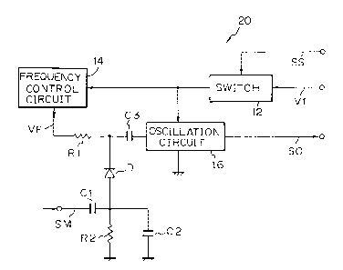
Referring to Fig. 3, an angle modulator embodying the
present invention and free from the above drawback is shown in a
2 0 block diagram. In this figure, the same or similar structural
elements as those shown in Fig. 1 are designated by like reference
numerals. The modulator of the present invention, generally 20,
comprises a switch 12 which is opened and closed by a start
control signal SS, a frequency control circuit 14 applied with a
2 5 source voltage V1 via the switch 12 for producing a frequency
control voltage VF, an oscillation circuit 16 also applied with the
source voltage V1 via the switch 12 for oscillating an output
signal SO, and a variable capacitance diode D which is connected
at one terminal (cathode) to the frequency control circuit 14 ~ia
30 a resistor R1 and to the oscillation circuit 16 via a capacitor C3
and, at the other terminal (anode) to ground via a parallel
connection of a resistor R2 and a capacitor C2. An input
modulating signal SM is applied via a coupling capacitor C1 to the
anode of the diode D. It is to be noted that the switch 12,
3 5 frequency control circuit 14, oscillation circuit 16, diode D,
1335826
resistor R1, capacitor Cl and capacitor C3 are identical in
construction and operation with those of the prior art modulator,
as shown in Fig. 1.
The capacitor C2 is provided with capacitance which is such
5 that the impedance of the capacitor C2 becomes low at the
frequency of the output signal SO and becomes high at the
frequency of the modulating signal SM. The resistor R2
constitutes terminating resistance for the signal SM. At the
frequency of the output signal SO, because the cathode of the
10 diode D is connected to a resonant circuit associated with the
oscillation circuit 16 via the capacitor C3 while the anode of the
same is grounded via the capacitor C2, the frequency of the
signal SO varies with the capacitance of the diode D. Since the
direct current flowing from the cathode of the diode D to the
15 anode is negligibly small, the voltage impressed across the diode
D is equal to the frequency control voltage VF. At the frequency
of the modulating signal SM, the cathode of the diode D remains
constant in voltage, VF, and the anode of the diode D is applied
with the modulating signal SM via the capacitor C2, so that the
20 signal SM is applied across the diode D. It follows that the center
frequency of the signal SO is tuned to the prescribed one by the
frequency control voltage VF and modulated in frequencY by the
input signal SM.
Fig. 4 shows a graph representative of a frequency-to-time
2 5 characteristic of the output signal SO in accordance with the
embodiment of Fig. 3. Because the capacitance of the diode D is
very small and so is the capacitance of the capacitor C3, the
frequency control voltage VF left the frequency control circuit 14
reaches the diode D immediately if the time constant for the
3 0 capacitors D and C3 to be charged via the resistor Rl is
neglected. Hence, assuming that the modulator 2 0 of Fig. 3 is
started up at a time ts, the center frequency of the output signal
SO is controlled to the prescribed one fc instantaneously, as
shown in Fig. 4.
3 5 Referring to Fig. 5, exemplary radio equipment with the
1335826
angle modulator 20 of the present invention is shown. The
equipment, generally 30, is provided with the angle modulator
20, a battery saving control circuit 32, a baseband circuit 34,
frequency synthesizers 36 and 42, a power amplifier 38, a
temperature compensated crystal oscillator 40, a receiver 44, a
duplexer 46, an antenna 48, a microphone 50 and a speaker 52,
which are connected as shown in the figure.
In the equipment, the battery saving control circuit 32
provides a control signal corresponding to the above-mentioned
control signal SS. In response to the ON/OFF control signal, a
switch (not shown) feeds the voltage of a power source (not
shown~ to the circuits 20, 34, 36, 38, 40, 42 and 44 to activate
them. In such a state, an audio signal picked up by the
microphone 50 is applied as the modulating signal SM to the
modulator 20 via the baseband circuit 34 including an audio
amplifier and a filter.
In the modulator 20, the switch 12 (Fig. 3) is opened and
closed in response to the control signal SS to control the supply of
the voltage Vl of the power source to the circuits 14 and 16.
Upon the closing of the switch 12, the oscillator 16 provides an
angle- modulated output signal SO which is converted by the
frequency synthesizer 36 and amplified by the power amplifier
38. The output of the amplifier 38 is sent to remotely located
radio equipment via the duplexer 46 and the antenna 48.
The radio signal sent from the remotely located radio
equipment is picked by the antenna 48 and received by the
receiver 44 via the duplexer 46. The receiver 44 frequency-
converts and demodulates the radio signal with the output of the
synthesizer 42. The demodulated signal is amplified by another
amplifier included in the baseband circuit 34, and sounded by the
speaker 52.
In summary, it will be seen that the present invention
provides an angle modulator which allows the center frequency of
its output signal to be rapidly tuned to a predetermined one after
35 a start-up of the modulator. This unprecedented advantage is
133~826
derived from a unique construction wherein a frequency control
voltage and an input modulating signal are applied to individual
terminals of a variable capacitance diode, so that the period of
time necessary for the frequency control voltage to reach the
5 diode is shortened without being effected by a coupling capacitor
which is adapted for the modulating signal and provided with
great capacitance. The present invention will prove particularly
effective when applied to an angle modulator which is operated
intermittently, e. g. a one which is built in a radio equipment
10 having a battery saving feature.
Various modifications will become possible for those skilled in
the art after receiving the teachings of the present disclosure
without departing from the scope thereof.