Note: Descriptions are shown in the official language in which they were submitted.
1 335955
HIGH Tc SUPERCONDUCTOR - GALLATE
CRYSTAL STRUCTURES
BACKGROUND OF THE INVENTION
Field of the Invention
This invention relates to high Tc superconductor
films deposited on gallate substrates, and more
particularly to such film - substrate combinations
which are suitable for device structures at
temperatures above 77 K.
Description of the Prior Art
The discovery of high temperature
superconductivity in copper oxide based materials
by Mueller and Bednorz in 1986 has been followed
by many advances based on their discovery. Thus,
the superconducting transition temperature has
been raised to approximately 125 K in a thallium-
based copper oxide (S.S.A.Parkin et al., submitted
to Phys. Rev. Lett., March 11, 1988). The initial
discovery of a thallium-based superconductor by
researchers at the University of Arkansas was
announced at the World Congress on
Superconductivity, held in Houston, Texas,
February 22 - 2~, 1988. Just prior to this,
researchers headed by H. Maeda at the National
Research Institute for Metals, Tsukuba, Japan had
announced a superconducting compound of bismuth,
YO988-029
~.
~d
-
1 335955
calcium, strontium, copper, and oxygen showing
evidence of superconductivity at about 105 K. A
few days after this, Paul Chu at the University of
Houston announced a substantially identical
compound except that it contained an additional
element - aluminum.
Prior to the discovery of the bismuth-based copper
oxide and the thallium-based copper oxide
superconductors, most of the work in this
technology had been centered on rare earth copper
oxides and in particular on yttrium barium copper
oxide superconductors having a transition
temperature of about 95 K. These materials were
typically known as 1-2-3 compounds because of the
atomic ratio Y-Ba-Cu in the superconducting phase
of these materials.
All of these copper oxide based superconductors
contain sheets, or planes, of copper oxide which
appear to be responsible for carrying the
supercurrents. However, the bismuth and
thallium-based compounds appear not to have the
copper oxide chains which are present in the rare
earth copper oxide superconductors and in the
yttrium 1-2-3 compounds. One of the
superconducting phases in the bismuth-based oxides
appears to be 2-1-2-2 (2 bismuth atoms, 1 calcium
atom, 2 strontium atoms and 2 copper atoms), while
the thallium-based superconductor contains
thallium, calcium, barium, copper and oxygen, the
superconducting material possibly having a 2-1-2-2
as well as a 2-2-2-3 superconducting phase.
YO988-029
1 335955
It is known in the art how to produce thin films
of high Tc superconducting material, and
specifically epitaxial superconducting films.
Such films have been made by several techniques
including electron beam evaporation, sputtering,
and solution pyrolysis. In particular, films of
high temperature copper oxide superconductors have
been produced on several substrates, including
SrTiO3, Si, Y - stabilized ZrO2, MgO, A12O3, and
various aluminates. To date, the best films have
been deposited on SrTiO3, these films being
produced epitaxially and with the highest critical
current density. Articles generally describing
thin film deposition of oxide superconductors
include the following:
1. M. Nastasi et al., J. Mater. Res. 2 (6),
p. 726, Nov/Dec. 1987.
2. M. Naito et al., Ibid, p. 713
3. R.B. Laibowitz et al., Phys. Rev. B 35
8821 (1987)
4. P. Chaudhari et al., Phys. Rev. Lett., 58
2684 (1987)
5. A. Gupta et al., Appl. Phys. Lett., 52,
163 (1988).
Although many substrates have been tried for the
preparation of high Tc oxide superconducting
films, the results to date have not been superior
in all respects. For example, it has not been
possible to deposit high quality epitaxial thin
films which are superconductive in their
as-deposited state. It has generally been the
YO988-029
1 33595~
situation that the film was amorphous or fine
grain polycrystalline as-deposited and
crystallized in a high temperature post annealing
step. This has been the method used to obtain the
highest quality epitaxial, high current density
films. Sometimes an annealing step is used to
convert the film from tetragonal to orthorhombic.
Since the lattice constants for these two
crystalline structures are quite far apart, the
required structural change has often produced
superconductng films that contain crystalline
twins, microcracks, and contamination. Thus, none
of the presently known substrates has offered the
possibility of direct deposition of a high
quality, high current density, high Tc
superconducting film without the additional
processing steps. This is especially true for the
1-2-3 films that are orthorhombic instead of
having 4-fold planar symmetry such as the readily
available substra~es MgO, SrTiO3 etc.
As mentioned, SrTiO3 has so far produced the best
superconducting copper oxide films. This
substrate provides a reasonable lattice match to
the superconductor films and can tolerate high
temperature annealing steps. However, large
quantities of Sr go into the superconducting film
during high temperature processing steps, and for
this reason the reactivity of this substrate is
quite high. Further, and more importantly, SrTiO3
has an extremely high dielectric constant which is
variable from sample to sample in accordance with
the substrate orientation and temperature, this
YO988-029
1 335955
material also being a very lossy dielectric. It
is difficult to produce using preferred
conventional crystal growth techniques such as
Czochralski or Bridgman techniques and costly to
produce by the Verneuil method. In addition to
the fabrication costs, it is very difficult to
obtain large area substrates of SrTiO3.
Si is a useful material for semiconductors, but
has a disadvantage in that it generally must be
passivated by a thin layer prior to the formation
of the high Tc oxide superconductor. This is
because the Si atoms tend to diffuse into the
superconductor and adversely affect its high Tc
superconductivity.
MgO is a substrate material whose dielectric
constant is very much less than that of SrTiO3;
however, it is not favorable for high temperature
annealing steps due to interdiffusion of Mg, and
can be difficult and expensive to prepare for the
deposition of a superconducting film thereon.
More importantly, its lattice constants do not
match well with superconducting copper oxide films
so that epitaxy is not favorable without other
techniques such as graphoepitaxy.
Y-stabilized zirconia is chemically better than
MgO at high temperatures, but inferior from a
dielectric loss viewpoint. Additionally, the
lattice match to the copper oxide superconducting
films is not favorable.
YO988-029
~= -
1 335955
Aluminates have also been used as substrate
materials, but these susbstrates are very
reactive, and the reactivity increases as the
processing temperatures increase. It has been
discovered that Al will replace Cu detrimentally
in the superconducting film to adversely affect
the superconducting properties. Additionally, the
spacing of atoms in the aluminates is too small to
give good lattice matches to the superconducting
10 film, regardless of the processing temperatures.
Thus, while thin films of high Tc oxide
superconductors have been made which in some
instances have yielded very high critical
currents, the presently known substrates all have
15 disadvantages which may preclude the use of
superconductive films in device structures.
Accordingly, it is a primary object of the present
invention to provide a class of materials which
can be used as substrates and interface layers for
20 the growth of films of high Tc oxide
superconductors having improved properties.
It is another object of the present invention to
provide high Tc copper oxide superconductor -
substrate combinations wherein high quality,
25 single crystal epitaxial superconductor films are
produced.
It is another object of the present invention to
provide high Tc oxide superconductor film -
substrate combinations suitable for use in
30 electrical devices.
YO988-029
~ 1 335955
It is another object of this invention to provide
high Tc copper oxide superconductor film -
substrate combinations which are particularly well
suited for analog and digital signal processing
devices.
It is a further object of this invention to
provide a class of improved substrate materials
for high Tc oxide superconductors where the
substrate material can advantageously be used as
an interlayer insulator in multilayer high Tc
superconducting devices.
It is another object of this invention to provide
epitaxial films of high Tc copper oxide
superconductors on substrates having good lattice
matching and good electrical properties for device
configurations.
It is another object of this invention to provide
favorable substrates and interlayer insulators for
perovskite high Tc superconductors.
It is another object of this invention to provide
improved perovskite superconductor - substrate
combinations.
It is another object of this invention to provide
superconducting perovskite - gallate combinations
which can be used in superconducting electrical
devices.
YO988-029
1 335955
It is another object of this invention to provide
highly oriented superconductive oxide films on
gallate substrates.
It is another object of this invention to provide
oxide superconductors - gallate substrate
combinations which have substantially matched
atomic spacings.
Brief Summary of the Invention
This invention relates to an improved class of
substrates and interface layers for high TC
superconducting perovskite materials, such as the
superconducting materials having Cu-O planes
therein which are responsible for carrying
supercurrents in these materials. Epitaxial films
of these high Tc superconductors can be deposited
on gallate substrates, where the substrates are
rare earth gallates or rare earth-like gallates.
These superconductor - substrate combinations are
particularly suited for analog and digital signal
processing devices including matched filters,
correlators, Fourier transformers, spectrum
analyzers, samplers, A/D converters, etc.
In general, the gallate substrate materials can be
grown by conventional techniques, such as the
Czochralski method or the Bridgman method, and are
cut to leave a wafer whose surface approximates
the primitive cubic perovskite (001) plane. This
provides excellent lattice matching to the copper
and oxygen atoms in the Cu-0 planes of copper
YO988-029
1 33595~
oxide superconducting films. These gallate
materials can also be deposited as films by
evaporation and sputtering, for use as insulating
interface layers, t-lnnel barriers, etc., in
combination with high Tc superconductors.
The high Tc superconductors used with these
gallate substrates are preferably those which
include Cu-O and Cu-O like current carrying planes
and can include rare earth and rare earth-like
elements, as well as combinations of these
elements. Also included are the non-rare earth
high Tc superconductors such as those having
Bi-Sr-Ca-Cu-O compositions and Tl-Ba-Ca-Cu-O
compositions. Gallates may also be used with
non-copper containing oxide superconductors,
although the degree of lattice matching may be
less than that when copper containing oxide
superconductors are used. Lattice matching of the
superconductor atomic spacing to the Ga-O plane is
especially good with the copper oxide
superconductors which form unique combinations
with these gallates.
These rare earth and rare earth-li~e gallate
substrates can be prepared in high quality crystal
form and provide excellent lattice matches to the
Cu-O based superconducting perovskites. This is
important in device applications since for oxide
materials misfit strains are extremely critical.
Additionally, these gallates can tolerate high
temperatures if necessary for the best quality
superconductor film growth and have relatively low
YO988-029
1 335955
dielectric constants and dielectric losses.
Further, they can be grown to large sizes by
standard crystal growth techniques. There appears
to be very little interdiffusion from the
substrates into the superconductor films so that
the properties of the superconductors are not
impaired even at high processing temperatures.
Both the substrate materials and the
superconductor films can be doped to modify their
properties and/or lattice constants.
These and other objects, features, and advantages
will be apparent ~rom the following more
particular description of the preferred
embodiments.
Brief Description of the Drawings
FIG. 1 illustrates a high Tc superconducting film
epitaxially deposited on a rare earth or rare
earth-like gallate substrate.
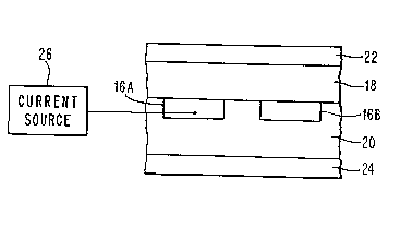
FIG. 2 illustrates a structure including a high Tc
superconducting strip line surrounded by a gallate
lattice-matched insulator, and further including
high Tc superconducting ground planes in a
structure suitable for electronic devices.
FIG. 3 illustrates the atomic arrangement of atoms
in a rare earth gallate substrate and atoms in a
Y-Ba-Cu-O deposited oriented superconductive film
YO988-029
~ 1 33~95~
showing the relative arrangement of the atoms and
the good lattice matches that result.
Detailed Description of the Preferred Embodiments
FIG. 1 illustrates a high Tc superconducting film
- substrate combination in which a
superconducting film 10 has been deposited on the
crystal substrate 12. A cooling means, if needed,
is not shown but is well known in the art.
Substrate 12 is a gallate substrate comprised of a
rare earth or rare earth-like element, gallium,
and oxygen. Examples include LaGaO3 and NdGaO3.
A mixed gallate can also be used, such as one
prepared from La-Y solid solutions. This
technique is used to provide different lattice
constants and to introduce different properties in
the substrate. The rare earth elements suitable
for use in the substrate include elements 58 - 71
of the periodic table, and in particular, Ce, Pr,
Nd, Sm, Eu, Gd, Tb, Dy, Ho, Er, Tm, Yb, and Lu.
The rare earth-like elements suitable for use in
the gallate substrates include Y, La, Bi and Sc.
As noted, combinations of these rare earth and
rare earth-like elements can also be used.
For the copper oxide superconductors the rare
z5 earth elements Tb, Dy, Ho, Er, Tm, Yb, and Lu may
not provide atomic spacings that give lattice
matches as favorable as those provided by gallates
YO988-029
1 335955
incorporating the rare earths Ce, Pr, Nd, Sm, Eu
and Gd.
The high Tc superconducting film 10 is one which
in preferred form is characterized by Cu-O planes
that are primarily responsible for carrying the
supercurrents in these materials. They generally
have a perovskite-related structure and can
include rare earth andtor rare earth-like
elements. These materials often include alkaline
earth elements, as for example Ca, Ba, Sr, Mg,
An example of a 92 K superconductor is the well
known YBa2CU3O7-X~ which is the s-called ~1-2-3
phase.
The superconducting film 10 can also be a copper
oxide composition which does not include a rare
earth element, but instead includes an element
such as Bi. A representative example is one in
the system Bi-Sr-Ca-Cu-O which exhibits a drop in
electrical resistance at about 115 K and a
transition to zero resistance at 85 K. Recentlv,
C. Michel and co-workers reported
superconductivity in the non-rare earth containing
Bi-Sr-Cu-O system. C. Michel et al., Z. Phys. B -
Condensed Matter, 68, 412 (1987).
A new BiSrCaCuOx composition was then found by
Maeda and Tanaka to exhibit high transition
temperatures with a resistivity completion in the
80 K range and a well defined resisitivity
decrease at about 115 K. This work is published
in the Japanese Journal of Physics, Vol. 27, p.
YO988-029
1 335955
L209 (1988). The work of Maeda, Tanaka et al. was
confirmed by C.W. Chu and co-workers, and by Hazen
and co-workers, these researchers noting the
structure and phase identification of this bismuth
- including copper oxide system. Reference is
made to R.M. Hazen et al., Physical Review
Letters, 60, p. 1174, (1988).
The new thallium - based superconductors can also
be used for the superconducting film 10. These
materials are usually in the 2-2-1-2 and/or
2-2-2-3 phases, these phases corresponding to the
relative amounts of Tl-Ba-Ca-Cu-O. For a further
discussion of these materials, reference is made
to M.A. Subramanian et al., Nature, Vol. 332, p.
420, March 31, 1988.
The substrate is prepared by well known crystal
growth techniques including the Czochralski
method, as well as Bridgman methods. The
superconducting films can be prepared by many film
deposition techniques including vapor transport
(such as electron beam co-deposition), single or
multiple target sputtering, and solution
pyrolysis, using different solution precursors
(such as nitrates). Generally, vacuum deposition
techniques tend to produce films which are oxygen
deficient. The films are annealed in an oxygen
atmosphere in order to obtain the correct
stoichiometry. The thallium and bismuth based
superconductors may not require slow cooling in an
oxygen atmosphere in order to incorporate the
correct stoichiometric amounts of oxygen. Any of
YO988-029
1 335955
these techniques can be used to deposit epitaxial
(oriented) films of the appropriate
superconductors, using starting materials that are
well known in the art. Prior to film deposition,
the surface of the substrate is mechanically and
chemically polished and/or annealed to provide a
clean crystalline surface. These polishing
techniques are also well known in the art and are
applied to other substrate materials, such as
silicon.
FIG. 2 shows a strip line structure of a type
suitable for use in superconductive analog or
digital signal processing devices. Devices of
this type are described in, for example:
S.A. Reible et al., IEEE Trans. Mag., Vol.
Mag - 19, No. 3, p. 475, May, 1983.
R.S. Withers et al., Ibid, p. 480.
A.C. Anderson et al., Ibid, p. 485.
In this structure, a superconducting strip line is
comprised of the patterned high Tc superconducting
lines 16A and 16B. These lines are surrounded by
the gallate insulators 18 and 20, which in turn
have high Tc superconductors 22 and 24 in contact
therewith. Superconductors 22 and 24 function as
ground planes for the signal lines 16A and 16B,
which are connected to the current source 26. To
make this structure the top half (gallate layer 18
and superconductor 20) is pressed into contact
with the bottom half (layers 16A, 16B, 20 and 24)
YO988-029
1 335955
and heated to provide the composite. Etching can
be used to provide grooves for the later
deposition of lines 16A, 16B.
The structure of FIG. 2 using superconducting
strip lines and associated ground planes is a
common structure of the type used in analog signal
processing devices. In the present invention, the
signal lines 16A and 16B can be patterned high Tc
oxide superconductors formed on a gallate
substrate having low dielectric constant and low
loss. Because of this, advantages result when the
structure is operated at temperatures near to or
in excess of 77 K, the temperature of liquid
nitrogen. Of course, device structures can also
be operated at temperatures less than 77 K.
Another device structure using gallates is a
tunnel device or Josephson device where a thin
gallate layer is evaporated or sputtered onto a
high Tc superconductor. The gallate layer can be
very thin (on the order of 20-50 angstroms) and
function as a tunnel barrier. Of course, gallate
layers of greater thickness, such as those shown
in FIG. 2, can be used as insulation layers in
combination with high Tc oxide superconductors.
TABLE I gives the lattice parameters for several
rare earth gallates while TABLE II gives the
lattice parameters of several high Tc
superconductors. Each of these TABLES is divided
~ into separate columns which consider the
YO988-029
1 335955
orthorhombic cell parameters as well as the
approximate equivalent primitive perovskite cell
parameters. The notes below TABLE I describe how
the parameters a, b, c, aO, bo~ and cO are
obtained. The Ga-Ga spacing in the a-b plane
(normal to the c-axis) of the substrate is
designated ac. This spacing is to register with
the Cu-Cu spacing in the associated plane of the
overlying superconductor film.
The data for the lattice parameters in TABLES I
and II are taken from publicly available
references. The references used for the data of
TABLE II include the following:
J.M. Tarascon et al., Phys. Rev. B 36, 226
(1987).
S.S.P. Parkin et al., submitted to Phys. Rev.
Lett., March 11, 1988.
M.A. Subramanian et al., Nature, Vol. 323, p.
420 (1988).
C.C. Torardi et al., Science, 240, p. 631,
(1988).
R.M. Hazen et al,, Phys. Rev. Lett., 60, p.
1174 (1988).
S.A. Sunshine et al., submitted to Phys. Rev.
Lett., February~ 1988.
YO988-029
1 335955
R~re Earth Gall Lte L~ Ce P3rameters
Appro cLmate eq~ivalent Ga-Ga
Orthorhombic cell p~Ll~h~ Perovslite cell parameters spal:ing
a~ bo 4 a b c a,
LaGaO3 5.496 5.524 7.787 3.886 3.906 3.894 3.896
CcGaO3 3.87 3.87 3.87 3.87
PrGaO3 S.46S 5.495 7.729 3.864 3.886 3.865 3.875
~IdGaO3 5.426 5.502 7.706 3.837 3.891 3.853 3.864
SmGaO3 5.369 5.520 7.650 3.796 3.903 3.825 3.850
EuGaO3 5.351 S.528 7.628 3.?84 3.909 3.814 3.847
GdGaO3 5.322 5.537 7.606 3.763 3.915 3.803 3.840
(SrTiO3 3 905 3 905 3.90S)
Notes
aO, b~, and cO are thc orthorhombic lattics p~ ~ "r~
a and b are a~ and bo divided by
c is cO divided by 2.
a~ is the Ga-Ga spacing in the ab plane which is to register with the Cu-Cu spacing in the ab plane
of the ;,u~.~n~--~r ~
The rare earth gallate data is taken from S. Gller, Acta Cryst. Vol. 10 (1957), pp. 243 - 251,
~Cryst~lk ~rhir Studies of Pe.ov~lLiL~-Like Co.~.pou~ds.'
REGATAB
High Tc Superconductor Lattice P~rameters
1 335955
Appro~imate equivalent
Supe~ ntl~l~or Tc Or~horhombic oell P~,.uv~ e oell
p~.,., . ~ t s p~ t; ,~
a b c= cO/n
YBa2Cu30,." 92 K 11.684 3.817 3.884
YBa2Cu3O.. r 92 K 11.657 3.8237 3.8874 3.886
LaBa2Cu307.r 92 K 11.783 3.8562 3.9057 3.928
NdBa,Cu3O7.r 92 K 11.736 3.8546 ~.9142 3.912
SmBa2Cu~O,.r 92 K 11.721 3.855 3.899 3.907
_uBa2Cu30,." 92 K 11.704 3.8448 3.9007 3.901
~R~,Cu,O,.r 92 K 11.703 3.8397 3.8987 3.901
DyBa2Cu3O7.r 92 K 11.668 3.8284 3.8888 3.889
HoBa2Cu3O7r 92 K 11.670 3.8221 3.8879 3.890
FrR~,CU3O7.r 92 K 11.659 3.8153 3.8847 3.886
TmR?2rU,O7.r 92 K 11.656 3.8101 3.8821 3.885
YbBa2cu3o7-r 92 K 11.650 3.7989 3.8727 3.883
~uBa2Cu~O7.r 92 K no~ reported
Tl2Ba2Ca Cu2Or ~118 K 29.39 3.857 3.857
112Ba2Ca,Cu2Or ~118 K 29.318 3.855 3.855
n2Ba2Ca2Cu,Or 125 K 36.23 3.821 3.821
TJ2Ba2Ca2Cu,Or 125 K 35.9 3.85 3.85
Tl,Ba2Ca2Cu30,~ -~110 K 15.871 3.8429 3.8429
Bi2Sr2CalCu2Or ~85 K 30.66 3.81 3.81
Bi2Sr2CalCu2Or ~85 K 5.41 5.44 30.78 3.82 3.85
Bi2Sr2Ca,Cu2Or ~85 K 30.6 3.817 3.817
Bi2Sr2Ca,Cu2Or ~85 K 5.414 5.418 30.89 3.828 3.831
Bi2Sr2Ca2Cu~Or ? ~110 K 30.7 3.82 3.82
I(e ~'
~ 1 3359~5
Particularly good lattice matches can be found,
for example, by matching the a-b plane of the
superconductors EuBa2Cu3O7_x and GdBa2Cu3O7_x onto
the a-b plane of a NdGaO3 substrate. Certain cuts
of the substrate NdGaO3 also seem to be quite
suitable for Tl-based superconductors.
Other cuts of rare earth gallate crystals in
addition to cuts perpendicular to the c-axis also
give good lattice matches to high Tc
superconductors having copper oxide planes. The
important factor is to expose a surface of the
substrate that approximates the square lattice of
the Cu-O sheets in the high Tc superconducting
materials. For example, substrate cuts along rare
earth orthorhombic 110 planes expose favorable
surfaces. An example of this that is particularly
favorable is a cut parallel to the 110 plane in
NdGaO3, which provides a good lattice match for
both the 2-2-2-3 and the 2-2-1-2 phases of
Tl-Ba-Ca-Cu-O superconductors.
It has been proven to be diffcult to stabilize the
approximately 110 K superconducting phase of
Bi-Sr-Ca-Cu-O superconductors. However, a
favorable epitaxial substrate chosen from the
class of gallates including a rare earth or rare
earth-like element may aid in stabilizing this and
other high Tc phases. A cut along the [110]
orthorhombic unit cell of GdGaO3 would expose a
surface with a favorable lattice match which may
provide stabilization.
YO988-029
~ 18
1 3359~
The use of these gallate substrates has not led to
adverse diffusion of Ga into the epitaxial
superconductors. Although some diffusion may
exist at high temperatures, the properties of
these epitaxial films are substantially similar to
those of pure superconductor materials.
As noted previously, the substrate is chosen to
give a good lattice match to the atoms of the
epitaxial superconductor film. While it is
customary to use substrates having a and b axes in
the plane of the substrate, it will be appreciated
by those of skill in the art that the b-c axes and
the a-c axes can be in the plane of the substrate.
As an example, an a-b cut of a boule of NdGaO3 can
be used as a substrate for a superconducting
epitaxial film of Gd-Ba-Cu-O having a 1-2-3 phase.
Another example, noted earlier, is an a-c cut in a
boule of NdGaO3 material to provide a suitable
substrate for the Tl-based superconductors.
FIG. 3 illustrates the relative placement of the
unit cell of a representative superconducting thin
film on a rare earth gallium oxide substrate. In
this example, the superconducting film is
YBa2Cu3O7 x which is deposited on a
perovskite-type rare earth (RE) gallate REGaO3.
For this epitaxial orientation, the unit cell of
the superconducting thin film is rotated 45 with
respect to the unit cell of the REGaO3 substrate.
In FIG. 3, the crystallographic axes are shown, as
well as the orthorhombic cell parameters aO, bo~
YO988-029
19
1 33595~
and c0. Also shown are the equivalent cubic
perovskite parameters a, b, and c, as well as the
Ga-Ga spacing c0. These quantities all correspond
to the like-labelled parameters in the foregoing
tables.
While the unit cell of this superconducting thin
film is rotated 45 with respect to the unit cell
of the perovskite substrate, such rotation will
not be needed for epitaxial matches of different
superconductors to the rare earth and rare
earth-like gallate substrates. One of skill in
the art would use an orientation of the substrate
such that good epitaxy and lattice matching will
occur with the chosen superconducting film. In
this example, the a and b axes are in the plane of
the substrate while the c axis is normal to the
substrate surface. However, some lattice matches
may be enhanced for epitaxy if, for example, the b
and c axes or the a and c axes were in-plane.
Regardless of the conventional notation used to
describe crystal systems, it is preferred to have
an arrangement OL the atoms on the substrate
surface which approximates a (100) cubic
perovskite surface. With this as a guide, the
substrate boule material is cut to provide the
desired orientation.
It has been noted that the gallate substrates
including a rare earth element or a rare
earth-like element exhibit good hardness and
tolerance to high temperatures. However, it may
be preferable to process the superconducting film
YO988-029
- - -
-
~ 3359~;5
at temperatures less than the
rhombohedral-orthorhombic transition of the
substrate in order to maintain the slight
orthorhombicity of the substrate. For LaGaO3, this
temperature is about 815 C.
The classic perovskite crystallographic structure
gives the atomic positions in a unit cell for
CaTiO3, a naturally occuring mineral, where Ca
usually has twelve oxygen neighbors and Ti has
six. All of the presently known superconducting
copper oxide compounds contain perovskite-type
cells as building blocks where Cu ions replace the
Ti ions of the CaTiO3 perovskite and Ca is
replaced mainly by rare earths Y, or Ba and Sr.
YBa2Cu3O7 x' in the 1-2-3 phase, has a basic unit
cell as shown in FIG. 3, having two Ba cuprate
perovskite cells that extend laterally into layers
normal to the vertical c - axis, with a Y cuprate
cell layer sandwiched between them. These three
layers are repeated along the c axis to build a
crystal. All of the superconducting cuprates
known have perovskite blocks arranged in planes
with continuous CuO2 sheets that are the pathways
of superconduction. In the 1-2-3 material
illustrated in FIG. 3, it is the neighboring CuO2
sheets between Y and Ba cuprate cells that support
superconductivity.
Accordingly, to grow epitaxial films with
desirable superconduct~ng properties the c - axis
is preferably normal to the substrate interface
which should contain (001) oriented perovskite
YO988-029
1 335 95S
cell cation arrangements, or atomic arrays that
the superconducting layer atoms will interpret as
such. Another way of specifying this is to say
that a good surface substrate layer has a simple
perovskite plane containing the a and b axes.
The cuprate superconducting oxides contain a basic
perovskite cell with a lattice constant of about
0.39 nm, so preferred substrates should contain a
matching perovskite cell in their structure. The
rare earth gallate perovskites, particularly the
lighter rare earth gallates of La and Nd, satisfy
this requirement. La is first in the rare earth
series and Gd is in the middle. La3+ ions are
larger than Gd3 ions. Gallates of the rare earth
elements from La to Gd are potentially useful as
superconducting oxide substrates. There is a
tendency for the heavier rare earth gallates to be
less stable in the perovskite phase for a 1:1
ratio of RE:Ga. For example, GdGaO3 perovskite
tends to decompose to other forms of the
constituent oxides. However, special known
annealing procedures can be used to stabilize
gallates having these tendencies.
As an example, YBa2Cu3Ox films were epitaxially
deposited on chemically polished LaGaO3 crystal
wafers by Rf sputtering, electron beam
evaporation, and trifluoroacetate hydrolysis, with
subsequent annealing at temperatures less than
1150 K. These films are epitaxial with their c -
axis normal to the growth interface. Film
textures are influenced by the orthorhombic
Yosss-02s
22
1 3~9~
perovskite substrate. Films have been deposited
having zero resistance at about 90 K and high
current densities in excess of 10kA/cm2 at 77 K.
The substrate had a dielectric constant of 25 at
room temperature and a low dielectric loss tangent
of about 0.0001. The LaGaO3 substrates were
easier to polish than SrTiO3, and were no more
reactive with the superconducting films when high
temperature annealing occurred at temperatures
less than 1150 K. There was some evidence for Ga
diffusion into the superconducting films; however,
the Tc values were very close to those observed
for pure YBa2CU37_x
In further examples, YBa2Cu3O7_x has been
reproducibly grown on LaGaO3 having [110] and
[100] oriented (primitive perovskite cell) single
crystal substrates. Three deposition techniques
have been used.
The LaGaO3 substrate has a distorted perovskite
structure and can be described by considering
layers of atoms parallel to the (001) planes.
There are four such layers in the unit cell as
schematically illustrated in FIG. 3. Two layers
contain La and O, with the O ions located at the
four corners and the center of the nearly square
layer. The La ions are located between the corner
O ions. The other two layers contain Ga and O,
with the Ga ions at the four corners and the
center of the layer. The O ions are located
between Ga ions, on segments which connect the
corner Ga ions to the center ion.
YO988-029
~ 1 335955
For these substrates, a LaGaO3 single crystal
boule was used that was grown to a size of 20 mm
in diameter x 90 mm long in the [100~ growth
direction. Slices of this boule were cut along
the ~110], ~100~ and ~010] primitive cell
directions.
The YBa2Cu3O7 x superconducting films were
deposited on these substrates by three techniques:
single-target oxide RF magnetron sputtering,
spin-on trifluoracetate tTFA) pyrolysis, and three
pocket electron beam evaporation. For each
deposition technique, smooth superconducting films
were obtained having varying thicknesses depending
upon the growth technique. For the sputtered
films, the superconducting film thicknesses were
0.4 - 0.92 micrometers which were completely
superconducting by 90.6 K. The critical current
for these films at 5 K is 5 x 10⁵A/cm2.
The second technique utilized TFA solutions to
make fluoride precursor films of YBa2Cu3O7 x that
convert to the desired oxides when heated to about
1100 K in helium/water and slow-cooled in oxygen.
The product thin films were 1-3 micrometers thick
and exhibited zero resistance at 90 K.
The superconducting films produced by the electron
beam evaporation system were 0.8 - 1 micrometers
thick and were annealed in helium and oxygen at
950 C and slowly cooled in oxygen to room
temperature. The Tc was complete for these films
by 87 K.
YO988-029
24
1 335955
The single target sputtering technique is
described in a paper by R.L. Sandstrom et al.,
submitted to Appl. Phys. Lett., 1988. The spin-on
pyrolysis technique is described by A. Gupta et
al., in Appl. Phys. Lett. 52, 163 (1988). The
three pocket electron beam system is described by
R.B. Laibowitz et al., in Phys. Rev. B35, 8821
(1987), as well as in Phys. Rev. Lett. 58, 2684
(1987).
In the practice of this invention, highly oriented
films of high Tc oxide superconductors have been
deposited on gallate substrates. These substrates
are those which include at least one rare earth
element or rare earth-like element. The
superconducting epitaxial films are highly
oriented and can approximate single crystals.
In the further practice of this invention, these
high Tc oxide superconducting film - gallate
substrate combinations are particularly suitable
for use in electronic devices including analog
signal processors, digital devices, A/D
converters, samplers, and Josephson devices.
It has also been found that these gallate
substrates are harder than commonly used SrTiO3
substrates and are easier to mechanically and
chemically polish. Additionally, their thermal
expansion coefficients match well to the oxide
high Tc superconductors.
YO988-029
~ 1 335955
While the invention has been described with
respect to particular embodiments thereof, it will
be apparent to those of skill in the art that
variations can be made therein without departing
from the spirit and scope of the present
invention. For example, the gallate substrate
materials may include combinations of rare earth
elements and rare earth-like elements, and may
also be doped to slightly vary lattice parameters.
Further, the superconductive films deposited on
these substrates, while preferably being copper
oxide-based superconductors, can include rare
earth elements, rare earth-like elements, and
alkaline earth elements. Still further,
combinations of these elements may be present and,
also, rare earth elements need not be present in
the superconducting film.
The best epitaxial matches occur when the
superconducting film is a copper oxide based film
where the Cu-Cu spacing is substantially matched
to the Ga-Ga spacing in the substrate. These Cu
oxide superconductor - gallate combinations have
special advantages based on these good lattice
matches and are considered unique combinations
that are suitable for device configurations of
many types. Highly oriented superconductive
layers are formed on these gallates and can be
epitaxial with the gallates. While it is
preferable to have single crystal gallates and
superconductive films, it will be appreciated by
those of skill in the art that the invention
encompasses the use of these gallate layers in
YO988-029
26
-
~ 1 335955
combination with oxide and copper oxide based
superconductive films, and is not limited to
either single crystal or epitaxial superconductive
film - gallate combinations.
YO988-029