Note: Descriptions are shown in the official language in which they were submitted.
1 3 3 6 1 0 3
DATA RE~lV~ INTERFACE CIRCUIT
Field of the Invention
This invention relates generally to a data
receiver interface circuit and more particularly to a method
and apparatus for accepting data which is correctly framed
within predetermined criteria.
Back~,o~,d of the Invention
Many data transmission systems send and receive
framed serial data. Each frame of data is identified with a
frame pulse that separates it from the preceding frame of
data. This frame boundary may be used for alignment of the
data being transmitted. For example, when a stream of bits is
being transmitted in a multi-channel arrangement, where each
channel has ten bits, the first bit represents bit 1 of
channel 1, the second bit represents bit 2 of channel 1... the
10th bit represents bit 10 of channel 1 and the 11th bit
represents bit 1 of channel 2. The first bit of each channel
is a frame pulse and bits 2 to 10 are typically comprised of
data bits, however some schemes may provide for bit 2 of each
respective channel to be used for verification such as parity.
A receiver receiving the serial stream of bits uses the frame
pulses for aligning the data bits with their respective
channels. Thus frame pulses are used to demark the boundary
of clusters of data and provide the receiver with a frame of
reference.
The transmission of framed data is shown in a
prior art elastic storage circuit for use in a telephone
switching system described in United States patent bearing the
number 4,323,790 in the name of Stephen C. Dunning et al.
This circuit employs a means of detecting first-in first-out
(FIF0) memory overflow or underflow due to a chronic increase
or decrease in the frequency rate of the data. The FIF0
temporarily stores the data portion of a serial stream having
been framed by frame pulses. This circuit does not provide a
means of monitoring data corruption.
- 2 ~ 336 1 03
Data is said to be correctly framed when the
number of clock cycles between pairs of successive frame
pulses is equal to a predetermined number. However, it is not
uncommon for corrupt data to be received at a node of a
transmission system; the cause of the data corruption may be
unstable clock sources, noise in the system, poor connections,
or a myriad of other causes. Often, it is found that extra
clock cycles or too few clock cycles occur between two
successive frame pulses in a system where the train of frame
pulses should be periodic and thus have a predetermined number
of clock cycles between each pair thereof. If this situation
goes undetected a large amount of corrupt data may be accepted
by the receiver before an error control mechanism is able to
detect the problem and initiate corrective action. Most of
the known data receivers use an input stage that includes an
elastic buffer usually in the form of a FIFO. Presently
available commercial FIFOs commonly provide fifo-full and
fifo-empty indications to denote overflow and underflow
conditions as well as read and write pointers. However it is
not possible to use the read and write pointers to monitor the
contents of the FIFO since they are internal to the devices.
It is thus an object of the invention to provide a
novel circuit and method for accepting correctly framed data
by detecting if the number of clock cycles between two
successive frame pulses is equal to a predetermined number,
and accepting the data if the number of clock cycles is equal
to the predetermined number.
Summary of the Invention
In accordance with the invention, there is
provided a method of accepting correctly framed data
comprising the steps of storing the data in a storage device,
counting the number of clock cycles that occur between
successive frame pulses, and accepting the stored data if the
number of clock cycles equals a predetermined number.
From another aspect, the invention provides a
circuit for accepting correctly framed data. A storing means
receives and stores incoming data and a counting means is
3 ~336~3
responsive to the received data for providing a count
corresponding to the number of bits between each pair of
successive frame pulses. A control circuit compares the count
with a predetermined number and provides an output signal upon
correlation thereof. The data in the storing means is then
released to a data receiver.
Detailed Description of the Preferred Embodiment
An embodiment of the invention will now be
described in conjunction with the drawings in which:
Figure 1 is a block diagram of the data accepting
circuit of the present invention; and
Figures 2A and 2B are state diagrams of a
read-write finite state machine (R/W-FSM) and a reset finite
state machine (R-FSM) respectively, illustrating the operation
of the circuit of figure 1.
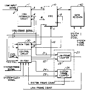
Referring now to figure 1, a link-interface
circuit 1 is shown having a data input terminal 2 for
receiving an input signal from a data link. The input signal
is a biphase encoded signal having data periodically framed
within successive frame pulses. As is generally known, a
biphase encoded signal encodes data, framing information, and
clocking information which may be recovered therefrom. The
encoding is as follows: a logic 1 is encoded as 0,1, a logic 0
is encoded as 1,0 and a biphase violation representing a frame
pulse is encoded as three consecutive ones or zeros. Since
the link input signal is typically a serial stream of bits
having data bits and frame bits serially combined, it is
necessary to separate the data bits and the frame bits. As is
well known in the art and exemplified in United States patent
4,323,790, the interface circuit 1 shown in figure 1 provides
a means for receiving the link data input signal and for
separately recovering data, clock and framing information.
The link interface circuit 1 has a first output terminal 3 for
providing a link-data signal, a second output terminal 4 for
providing a link-clock signal and a third output terminal 5
for providing a link-frame signal. These three signals are
derived from the composite link input signal.
4 1 3361 ~3
A data receiver 40 reads data quasi-synchronously.
A quasi-synchronous arrangement is one wherein a receiver and
transmitter have clock signals of the same frequency however
communication between the transmitter and receiver is
asynchronous. Typically, an elastic buffer such as a first-in
first-out buffer is used to temporarily store data in an
asynchronous communications scheme.
A first-in first-out buffer (FIFO) 10 has an input
terminal 6 connected to the data output terminal 3 of the
interface circuit 1 and serves to temporarily store a portion
of the link data signal which may then be outputted on
terminal 7 to a data receiver 40. As is conventional for such
devices, the FIFO 10 has a fifo-full terminal 8 and a
fifo-empty terminal 9, a reset terminal 11, a read terminal R
and a write terminal W. A control circuit 30 is adapted to
control the operation of the FIFO 10 in response to signals
from the interface circuit 1, a counting circuit means 20 and
the FIFO 10. The control circuit 30 is connected to the
output terminals 4 and 5 of the interface circuit 1 for
receiving the derived link-clock signal and the derived link
frame signal respectively. In order for the data receiver 40
to function with the circuit of the invention, it provides the
control circuit 30 with a system-clock signal having the same
frequency as the link-clock signal and a system-frame signal
having the same frequency as the link-frame signal.
The control circuit 30 is basically a network of
logic gates interconnected to output predetermined control
signals when predetermined input signals are asserted. The
circuit 30 may therefore be considered to be a finite state
machine (FSM). In fact the control circuit 30 may be
logically divided into a read/write state machine (R/W-FSM)
and a reset state machine (R-FSM) as shown in figure 1.
The counting circuit means 20 has first and
second counters 25 and 26 for counting clock cycles within any
given frame of data. The first counter 25 is responsive to
the link-clock signal on line 21 and a delayed-link-frame
signal on a first clear line 22 to generate a link frame count
representing the number of clock cycles between frame pulses
- 5 l 3361 ~3
in the link input signal. Similarly, the second counter 26 is
responsive to a system clock signal on input line 23 and a
delayed-system-frame signal on input line 24 to generate a
system frame count representing the number of system clock
signals that exist between system frame pulses in the system
frame signal. Both the delayed-link-frame and the delayed-
system-frame signals are derived from the link-frame and
system-frame signals respectively in control circuit 30, and
they follow their respective original signal in time, being
shifted in time from them by one clock cycle. The counters 25
and 26 provide their respective output signals to the control
circuit 30.
The counter 26 and related circuitry serve to
monitor the operational relationship between the data receiver
40 and the FIFO 10 by insuring that the receiver is capable of
reading the contents of the FIFO properly.
In operation, the link interface circuit 1
receives the link input signal which, as discussed above, is a
composite serial signal composed of data and frame bits as
well as clocking information. The interface circuit 1 decodes
the received signal into the link-data signal, the link-clock
signal and the link-frame signal. The control circuit 30
receives the link-clock signal, the link-frame signal, the
system clock signal, the system-frame signal, the fifo-full
signal, the fifo-empty signal, the link and system frame
counts, and generates the write, read or reset signals to the
FIFO 10 in dependence upon the state of the received signals.
When the write signal is asserted, the FIFO 10 receives the
link-data signal and stores data bits sequentially until the
read signal or the reset signal is asserted. Upon assertion
of the read signal the data bits are read out of the FIFO 10
by the data receiver 40. The FIFO 10 is used as a temporary
buffer to store the data while the control circuit 30
determines if the data is correctly framed. When the reset
signal is asserted, the FIFO 10 flushes all its data. This
process of flushing may simply be achieved by resetting the
read and write pointers within the FIFO 10 instead of actually
erasing the stored data.
1 3361 03
The first and second counters 25 and 26 operate in
the same manner but have different input and output signals.
The count of the first counter 25 is incremented by the link
clock signal and is reset upon assertion of the delayed-link
frame signal which is generated by the control circuit 30.
The control circuit 30, in response to the link-frame signal
compares the count represented by the link frame count to a
predetermined number. If the count and the predetermined
number are equal, the read signal is generated by the control
circuit 30 in dependence upon the system-clock signal and the
system-frame signal being asserted, and data stored in the
FIFO 10 may be read. The count of the second counter 26 is
incremented by the system-clock signal and the second counter
is reset upon assertion of the delayed-system-frame signal.
Before generating the read signal the integrity of the system-
frame signal is verified by determining if the system-frame
signal has the correct number of clock cycles between
successive frame pulses. If the number of clock cycles
between frame pulses is incorrect, the control circuit 30
generates the reset signal to clear the contents of the FIFO
10 .
The following description of operation may be
better understood by reference to figure 2A which illustrates
the functions of the R/W-FSM and figure 2B which illustrates
the functions of the R-FSM.
The following pseudo code represents the operation
of the R/W-FSM:
State 0: read signal not generated
write signal not generated
READING=false
If no reset present
if link-frame signal present go to State 1
else go to State O
State 1: read signal not generated
write signal generated
READING=false
if no reset present
if system-frame signal present go to State 2
else idle waiting for system-frame signal
else go to State O
_ 7 l 3361 03
State 2: read signal generated
write signal generated
READING=true
if no reset present go to State 2
else go to State 0
The read/write FSM will wait in State 0 after the reset signal
has been asserted until the link-frame signal is present.
When the first link-frame pulse occurs the R/W-FSM will assert
the write signal and data will be written into the FIFO. If
the system-frame signal is generated, State 2 is executed from
State 1 and the FIFO is read.
The following pseudo code represents the operation
of the reset FSM.
State 0: If READING = true and fifo-empty asserted then go
to State 3;
if fifo-full go to State 3
if link-frame signal present go to State 1
if system-frame signal present go to State 2
go to State 0
State 1: if link_frame_count not equal to
predetermined_value
then go to State 3
else go to State 0
State 2: if system_frame_count not equal to
predetermined_value then go to State 3
else go to State 0
30 State 3: Reset_read/write_FSM = true
go to State 4
State 4: Reset signal = true
go to State 5
State 5: Reset signal = false
go to State 6
State 6: Reset_read/write_FSM = false
go to State 7
State 7: if link-frame signal present go to State 8
else go to State 7
5 State 8: if system-frame signal present go to State 0
else go to State 8
State 0 is the idle state wherein the R-FSM is
monitoring for either full or empty conditions. State 1 and 2
go to state 3 if the link frame count is not equal to the
1 336 1 03
_ 8
predetermined value. State 3 and 6 are error states. The
reset_read/write FSM signal first resets the R/W-FSM and the
assertion of the reset signal resets the FIFO. States 7 and 8
wait until the start of the next frame before going back to
the idle state 0.
Conveniently the control circuit 30 may be
realized using one or more programmable logic arrays suitably
configured to function as the R/W-FSM and R-FSM. Similarly
the counters 25 and 26 may be realized using the same or
another programmable logic array.
The circuit of the invention therefore allows a
data link interface circuit that uses a commercially available
monolithic FIFO to accept correctly framed data.
With the addition of a minimal amount of circuitry
to a conventional data receiver interface circuit, the
invention provides an economic and effective way of rejecting
corrupt data due to incorrect framing.