Note: Descriptions are shown in the official language in which they were submitted.
'-- 1 336 1 39
That this application is a division of Canadian
1 application Serial No. 614,898 filed September 29, 1989.
,
The invention described herein was made in
connection with wor}; performed under a ~rant or award from
the Division of Rescarch ~esources of the ~ational Institute
of Health.
The present invention relates to the field of
analytical chemistry, and particularly to the study of
fluorescence and phosphorese,nce phenomena in the biochemical,
biological and biophysical,arts.
The use of fluorescence spectroscopy for the study
of the dynamics of macromolecules is becoming more widespread
as more sophisticated instrumentation is being developed.
~lthough fluorescence spectroscopy has developed into a
widely accepted technique in the physical and chemical
sciences as well as in the biological sciences, the practical
utility of fluorescence methods is still limited by the
- availability of fluorescence spectroscopy instrumentation
capable of measuring such events accurately.
~ Fluorescence is the rapid decay from a higher to a
lower state of the same multiplicity. The natural time
window of fluorescence is suitable to resolve dynamic events
- occurring in the nanosecond (ns) to pico-second ~ps) time
region. The above characteristics, coupled with the
3o sensitivity of the excited state of a fluorophore to the
- p~ysicochemical properties of its environment, is a major
reason why fluorescence spectroscopy techniques are so
1~ ~
`Y ,!
, -2- 1 3 3 6 1 3 9
1 frequently used in the study of micro-biological structures
and functions.
The greatest interest is in measuring dynamic
events displayed in the kinetics of intensity decay
(fluorescence lifetimes) and anisotropy decay. The
fluorescence lifetime reflects not only the intrinsic
radiative rate of the excited state, but also the
interactions of the fluorophore with the environment.
-Anisotropy decay measures the displacement of the emission
transition dipole with time after excitation and thus
reflects the rotational motion of the fluorophore. The rate
and the amplitude of the rotational motion in a given time
are themselves dependent on the free volume, the microscopic
.. ~ . ....
viscosity of the local environment and the forces acting on
the excited molecule. Therefore, anisotropy decay indirectly
describes the structure and dynamics of the fluorbphore's
environment. Clearly, a detailed study of the fundamental
fluorescence observables (spectrum, quantum yield, lifetime
- and anisotropy) can provide substantial inf ormation about a
biological macromolecule and its surrounding. Additional
insight can be gained, if the system is physically or
chemically perturbed, for example, by temperature or
--- viscosity change or the presence of fluorescence ~uenching
agents. The frequently complex fluorescence signal from - -
biological systems does not easily yield to mathematical
analysis and it may be difficult to correlate a physical
event with the result of the analysis.
The time decay of fluorescence is usually measured
using one of two accepted, but different approaches.
Measurements of fluorescence decay can be made in the time
domain using the popular technique of correlated single
photon counting (SP~), or in the fre~uency domain by
1 336 1 39
1 determining the phase delay and the relative modulation of
the fluorescence signal with respect to the exciting light.
The modern study of fluorescence properties started with time
domain fluorometry and has evolved into methods using
frequency domain fluorometry. In the frequency domain, the
frequency axis is examined one point at a time, wh~le in the
time domain, the full decay is collected at once; however,
the collection of information in the time domain takes from
-several minutes to several hours depending upon the
excitation source, while in the frequency domain, the data
collection at a single frequency takes only a few seconds.
Therefore, it is possible in the frequency domain to acquire
an equivalent amount of information in a similar amount of
time. Indeed, a great advantage in the frequency domain can
be achieved if all frequencies can be collected at the same
time.
. l'he maximum time resolution of sequential
multifrequency phase fluorometers is about I or 2
picoseconds, which compares favorably with time correlated
single photon counting instruments. The decomposition of the
decay curve using a sum of exponentials, may also ~e obtained
from a multifrequency measurement applying a non-linear least
squares routine. The analysis of a double and triple
ex~onential decay may be performed on dedicated
micro-computers.
Xesolution of emission anisotropy decay is obtained
by a measurement of the differential phase and modulation
ratio of the horizontally and vertically polarized emission
components, arising from vertically polarized excitation.
This technique, originally developed for single modulation
frequency operation, has become extremely powerful when
coupled with a multifrequency phase fluorometer. Fast
1 3361 39
1 rotational correlation times on the order of 10 picoseconds
and longer can be measured. ResolUtion of anisotropic
rotational motions can also be obtained from a multifrequency
data set using a non-linear least squares analysis.
Restricted rotational motions can also be an21yzed. The
ability to perform direct differential measurement, such as
the phase delay between the perpendicular and the parallel
polarized components of the emissions, is a unique intrinsic
characteristic of phase fluorometry and results in an
improved time resolution.
Phase fluorometry has the intrinsic capzbility to
perform phase sensitive detection, which provides a simple
and powerful method to separate spectral components in a
mixture of fluorophores. T~ls separation is based on the
principle that each emitting species in the mixture has a
characteristic phase delay. The spectra of the overlapping
components can be obtained with a single scan using our new
approach of phase and modulation resolved spectra. This
simple approach requires no fitting of the data. The
resolution is instead obtained directly from the values of
the phase and modulation.
The prior art shows a num~er of examples of systems
utilizing frequency domain fluorometry techniques. The 1984
article "The-Measurement and Analysis of Heterogeneous
Emissions by Multi-frequency Phase and Modulation
Fluorometry`' by Jameson, Gratton, and Hall, Applied
Spectroscopy Reviews, 20(1), pages 55-106 (1984) discloses
two methods of multi-frequency phase and modulation
fluorometry as well as a commercially available fluorometer.
In addition, the article discloses a fluorometer the authors
developed for research purposes. The commercially developed
fluorometer, developed by SLM AMINC0, utilizes a xenon arc
~ 1 336i 39
l lamp to provide an excitation signal to generate the
fluorescence emissions. The light supplied by the arc lamp
is intensity modulated before impinging upon a sample to be
studied. The light emitted by the (study) sample is d~tected
by a photomultiplier, the last dynode of which is modulated
at a frequency equal to the light modulation frequency plus a
small additional frequency. This procedure is a
cross-correlation technique, wherein the phase and modulation
-information of the emitted signal is transposed to a mu_h
lower frequency range where it can be interrogated. Tne
phase delay and demodulation of the emitted signal relative
to the scattered light is then calculated. The research
fluorometer described in the'article is a variable fresuency
cross-correlation phase fluorometer which utilizes an argon
ion laser to provide an excitation beam to excite the
fluorescence action and to provide a reference signal. The
light supplied by the laser is sinusoidally modulated, and
split into two beams, one signal is used to excite the study
sample and the second signal is used as the reference signal.
The reference signal and the signal emitted by the study
sample are then passed through two photomultipliers wherein
the cross-correlation processing described abo~e is done.
The outputs from both photomultipliers are then passed
through identical sections of analog circuitry wherein the
data is sequentially processed and displayed.
The 1986 article "A Multi-Frequency Phase
Fluorometer using the Harmonic Content of a Mode Locked
Laser" by Alcala and Gratton, Analytical Instrumentation,
14(3 and 4), pages 225-250 (1985) discloses a
cross-correlation phase and modulation fluorometer which
utilizes the harmonic content of a high repetition rate, mode
locked laser. In t-he frequency domain a pulsed source
~ G- 1 336139
1 provides a large series of equally spaced harmonic
frequencies. The pulses from the laser are amplitude
modulated and frequency doubled. The signal is then split
into a reference beam and an excitation beam. The reference
5 beam is directed to a first phetomllltiplier and the
excitation beam is directed to a study sample and then the
emission from the sample is detected by a second
photomultiplier. The photomultipliers provide
-cross-correlated miY~ing which in addition to fre~uency
translation also allows transler of the phase and modulation
information desired at the individual harmonic frequencies.
The outputs from the photomultipliers are then passed through
various forms of analog filtering circuits and amplifiers
wherein the necessary phase and modulated data is
sequentially derived from the outputs of the
photomultipliers.
Frequency domain fluorometry in certain instances
has the advantage of the rapid determination of single or
double exponential fluorescence lifetimes which can be
o~tained by measurements at only one or two fre~uencies.
This is not possible for systems where complex fluorescence
decays must be resolved. In order to handle complex decays,
a large number of modulation frequencies is needed to obtain
the full decay information. The above disclosed fluorometers
provide this capability only to a limited extent.
The above referenced articles disclose fluorometers
that use frequency domain techniques as opposed to time
domain techniques. Frequency domain fluorometers have the
advantage of high accuracy and rapid determination of
fluorescence lifetimes. However, the above referenced
fluorometers utilize analog signal processing techniques
after data collecti-on. Unwanted effects on the signals of
~ 7-
~ 1 336 1 39
-
interest are caused by the bandwidth and non-linearity of the
analog filters used in the above referenced fluorometers. In
the analog electronics of most commercial frequency domain
fluorometers, six pole active filters are utilized to perform
5the necessary filtering functions. These filters are hard to
tune to the appropriate frequency, they suffer from thermal
and drifting problems and have undesirzble phase shift. The
accuracy of lifetime measurement is limited by the analog
signal processing portion of the fluorometers.
The present invention utilizes a computer
controlled digital acquisition system to cre2te a parallel
phase fluorometer which collects and processes several
harmonic frequencies simultanëously. The digital processing
15 functions used in the present invention provide for more
accurate filtering functions, parallel frequency acquisition,
and the ability to change filter functions in software at
mi ni m~l cost and requiring only a minimal time.
The present invention is directed to a digital
20 frequency domain fluorometer for measuring the fluorescent
response of a sample when excited by a pulsed light source.
The invention is basically comprised of two sections. The
- first section is a novel data acquisition section which is
capable of collecting spectral components of fluorescence
25 data in an x-y array. The second section is a parallel phase
fluorometer processing section which is responsible for
simultaneous processing the collected data value and to
provide useful information to the operator.
The data acquisition section basically involves
30 exciting a sample to be studied so as to cause the sample to
emit a fluorescent light. In one embodiment of the
invention, the emitted fluorescent light is captured and down
~!
t~
~ 8-- 1 3361 39
convcrted to a more manageabIe frequency using the sample and
ref~rence photomultiplier tubes which mix a cross-correlation
frequency therein. The correlation signal from the P~ is
now an electric signal as opposed to a light signal. The
5phase and modulation information from the response of the
sample is carried by a discrete waveform at the correlation
frequency, and may be processed by the parallel phase
fluorometer processing section of the invention.
In a second embodim2nt, a diode or CCD array is
10 coupled with a gatable means to analyze the spectral and
frequency response of tne sample at discrete x-y lo~ations.
The apparent time resolution of the diode array is enhanced
by a unique gating technique which cross-correlates a high
frequency source at f1 with an image intensifier at fl + fc
15 to optically cross-correlate the emission response phase and
modulation informa~ion onto fc. Tnis technique enables an
array, which nominally resolves in the milli-second range, to
time resolve events in the picosecond range, since the
frequency to be resolved which is f1, has been translated to
20 fc by the gating action of the image intensifier.
The parallel phase fluorometer processing section
ta~es the discrete waveform from either of the above
embodiments and digitally filters and processes it to eY.tract
the desired information. The desired information consists of
25 modulation and phase data with respect to the reference
signals. The digital filtering is done in software using
digital filtering techniques including averaging filtering
and fast fourier transforms (FFT).
The digital frequency domain fluorometer of the
30 present invention provides for the filtering and calculation
of the phase and modulation ratio of a fluorescence signal
from which the fluorescence lifetime of the decay can be
` 1 3 3 6 1 3 9
,
1 determined. In addition, by incorporating a computer for the
direct collcction of data and for the processing of the data,
the majority of systematic errors due to analog signal
processing circuits can be avoided or minimize~. The digital
acquisition method described herein allows for much better
si~nal filtering than the analog electronics currently used
in frequency domain fluorometers and also p~ovides for the
added capability of parallel frequency acquisition.
Among the advantages of the digital electronics is
the intrinsic cap~bility to modify the base filter frequency
by simply entering into the computer a different number for
the acquisition period. In this manner, it is possible to
determine the best cross-correlation frequency to be used on
the basis of the phase noise characteristic of the frequency
synthesizer.
The cost of the digital ac~uisition system is
substantially reduced relative to the cost of standard analog
systems. The off the shelf digitizing board used in the
described embodiment costs about $1,000, compared to at least
$10,000 for the analog electronics found in commercial
frequency domain fluorometers.
The improvements given by this new digital
electronic acquisition system can be summarized as: (1) a
factor of 10 in enhancement of filtering capabilities; (2) a
factor of 10 in reduction of ac~uisition time; and (3) a
fact~r of 10 in reduction of cost.
The present invention provides a new and practical
means to analyze complex fluorescence decays in real-time
using standard data collection technigues and digital
30 processing techniques. The invention is useful in the
analysis of multi-exponential decays, continuous lifetime
dist~ibutions, rotational rate determinations, resolution of
r
- - -10- 1 3361 39
1 spectral components, excited state reactions and energy
transfer and dipolar relaxations.
Figure 1 is a diagra~mztic illustration of one
embodiment of our invcntion using photomultiplier tubes for
cross-correlation mixing.
Figure 2 is a diagrammatic illustration of a second
embodiment of our invention using an improved array detector
for optical cross-correlation miY.ing.
Figure 3 is a schematic illustration of a current
to voltage converter and amplifier used to match the output
of the PMT tubes to a standard analog to digital converter.
Figure 4 is a diagrammatic illustration of the
~ array detector used in one e~bodiment of the invention.
Figure 5 is a schematic illustration of the circuit
used to insert the pulse and correlation frequency into the
array detector illustrated in Figure 4.
Figure 6 is a graph illustrating the preferred
biasing voltage between the image intensifier and the array
detector.
Figure 7 is a conceptual illustration of the direct
memory access portion of the invention.
Figure 8 is a simplified flow chart of the data
acquisition and data processing programs used in the present
invention.
Figure 9 is a graph illustrating the phase and
modulation value of P-terphenyl obtained with the present
invention.
Figure lOa is a graph illustrating the filter
response of the digital averaging filter using 10 seconds of
integration.
1 3 3 6 1 3 9
l Figure lOb is a graph illustrating the filter
response of the fast fourier transform using only the
fundamental frequency.
Figure lOc is a graphic illustrating the response
5 of the combined averaging filter and fast fourier transform
calculated for the fundamental frequency.
The present invention relates to improvements in
the field of frequency domain phase fluorometry. In one
lO embodiment, a pulsed light source having a predetermined
frequency and multiple harmonics is used .o simultaneously
excite a sample at a fundamental and a plurality of harmonic
~requencies. Improved digital acquisition and
. .
cross-correlation techniques enable the collection of the
15 phase and modulation information at each of the 'requencies
onto a single wave form. The ~ave form is digitally filtered
to remove non-harmonic and non-synchronous frequencies, and a
~ast fourier transform is performed on the filtered waveform.
The result is the simultaneous derivation of the
20 phase and modulation values of the sample response at a
plurality of frequencies from a single excitation.
In a second embodiment, the first embodiment is
used with an array detector capable of collecting discrete
values of the phase and modulation response at a plurality of
25 x-y locations, and at a plurality of various wave length or
color emissions to assist in resolving and imaging multiple
emissions from a single excitation.
The array detector provides an improvement over
known array devices in as much as it enables measurements of
30 the luminescence decay time in the pico-second to nano-second
range over the entire spectral emission band using correlated
gating techniques. The gating reduces the duty cycle of the
~ 12-
1 33S 7 3~
1 measurement, and extends the maximum resolution time to about
20-30 pico-seconds with a duty cycle of about 50%.
The time decay of fluorescence is typically
measured using one of two different approaches. The system
response to transient (pulsed) excit2tion can be cetermined
in the time domain by the popular technisue of time
correlated single photon counting. Alternatively, the
fluorescence response can be measured in the frequency
domain, by determining the phase delay and the relative
modulation of the fluorescence signal with respect to the
exciting light. The time domain and frequency domain
approaches provide equivalent information and are related to
each other by the fourier transform.
In the frequency domain the time variation of the
excitation light intensity is described by
E~t) = Eo(1 + Mesin(~t) (1)
~ here Eo and Me are the average value of the
intensity and the modulation of the excitation respecti~-ely.
The overall fluorescence response of the system to sinusoidal
e~citation can be written in the form
F(t) = Fo¦(1 ~ Mfsin(wt-0)] (2)
Where Fo and Mf are the average value of the
intensity and the modulation of the fluorescence,
respectively. For linear systems the emitted fluorescence
has the same modulation freguency but is demodulated and
phase-shifted with respect to the exciting light. The phase
delay and modulation ratio between the excitation and the
emission constitute the two independent measurable quantities
in phase fluorometry. The following equations relate these
parameters to the case of the pulse response, IF(t), to
excitation by a delta function at excitation frequency, w,
~ 13- 1 3361 39
S
tan ~ = G (3)
1~
M = Me = N 1(s2 + G2~1j2
wnere
,.,00
5 =J OIF(t)sin ~t dt (5)
G = ~oIF(t)cos ~t dt (6)
N ~o~F(t)dt.
Knowledge of ~ and ~ is equivalent to knowledge of
the functions S and G which correspond to the sine and cosine
fourier transforms of the ideal pulse response IF(t).
Consequently the measurement of phase and modulation as a
function of the frequency is equivalent to determining the
15 time evolution of the emitting system to delta pulse
excitation. In phase-mGdulation fluorometry, however,
deconvolution for the finite width of the eY~citation pulse
and the time response of the detection system is unnecessary
since the ideal pulse response is obtained.
Multiple frequency excitation has traditionally
been accomplished by using a synchrotron or pulsed laser
output at a plurality of frequencies. It is also known that
- pulsed light sources contains multiple harmonics, and that in
the frequency domain all of the photons in the light source
25 contribute to the measurement of each harmonic frequency.
The average signal measured at the i..th harmonic for very
narrow pulses has practically the same intensity as the
complete fluorescent signal.
Since the use of the preselected fundamental and
30 hanmonic frequencies obviates the need for sequentially
collecting separate measurements at each frequency, and the
attendant needs to tune and acquire "dark wave" reference
~ - -14-
1 3361 39
l signals at each frequen_y, its use is preferred in the
~ractice of this invention, except where the measurement of
fluorescent lifetime or rotational rate requires the use of a
f~-equency available only from a modulated source.
Cross-correlation in a phzse fluorometer was first
described by Spencer and ~eber in an article entitled
"Measurements of Sub-nano-second FluoresCenCe Lifetime with a
~ross-Correlation Phase Fluorometer", Ann. New York Acad.
Sci. (1969) p361. In the present invention, the operating
principle is the same, but it is ex~ended to cover the
harmonics in the cross-correlation signal. When a
fluorophore is excited by a pulsed light source, the
fluorescence has the same frëquencies as the excitation, but
each harmonic frequency is demodulated and phase shifted
differently with respect to the exciting light. Tne
modulation ratio, M, and the phase shift, ~, are related to
the fluorescence lifetime,7J, by
tan
Mf
M ~ M ~
.
where Mf and Me are the modulation of the fluorescence and
the excitation respectively. The frequency content of the
fluorescence can be written as
N
t) ---Fo[1 + ~ Mfncos (n~t ~ ~n)~
3o
where Fo is the average fluorescence. The cross-correlation
technique mixes the~fluorescence signal with a
1 336 1 39
1 cross-correlation signal, C(t), which is at a slightly
different base frequency, WC :
%
C(t) = CO [1 + ~l~cos (k~ct ~ ~k)]~
k=l
(9)
the resulting signal is the product of V(t)=F(t)- C(t).
N K
V(t~ = Fo Co[(l~ ~ Mfncos(n~t+~nl~ ~ Mckcos(k~ct+~)
N K ~
+ ~, Mfn cos(ncdt+~n)+ ~;Mckcos(kc~ct~)k)l]
The last term can be rewrittën using trigonometric
relationships as the sum and difference of the two
frequencies. If we loo~ at only the lowest frequency region,
with i=j, the only term remaining is:
~C (11)
~ co~(n~t+~
n=l
where ~ ~ Jj, This series ends at n=K since we
have assumed K <~, i.e. the cross-co~relation signal has less
- harmonic content than the fluorescence signal. This
expression contains all of the phase and modulation
information of the original fluorescence signal at all the
harmonic frequencies, now as harmonics of wc, but if WC is
very close to w, then this information is at much lower
frequencies that are easier to isolate and sample with our
digital electronics. In the embodiment illustrated in Figure
1 ~ ~ was set to 40 Hz. In the embodiment illustrated in
Figure 2, G f= w/2l is set to 15 or 7.5 Hz.
-16-
1 336 1 39
1 ~'or parallel phase fluorometrY, a high harmonic
content in both the light modulation and in the
cross-correlation signal is required. High repetition pulsed
sources, such as mode-locked lasers and synchrotron
radiation, intrinsically contain a high harmonic co~tent.
Traditionally, the cross-correlation product is ob~ained by
applying an appropriate voltage to one of the dynoces of the
photomultiplier tube. This internal miY.ing is quite
powerful, since the P~ itself is a very good mixer. The PMT
dynode chain produces good amplification with very low noise,
and it does not require any extra components. In 'he
embodiment illustrated in Figure 1, the mix.ing occurs in the
photomultiplier tube. In thé embodiment illustrated in
Figure 2, the mixing occurs in the light signal emitted by
the sample by a gating technique, prior to the sam?ling by
the diode array. A more complete explanation of the cross
correlation accompanies the detailed description of each
embodiment.
The parallel phase fluorometer illustrated in
Figure 1 has the intrinsic capability to separate out all of
the harmonic information contained in the cross-correlated
- signal. This capability can be exploited by using a light
source that has high harmonic content, such as a pulsed laser
25 system, or by pulsing the Pockel's cell modulator used in
most phase fluorometers and cross-correlating with a waveform
that contains harmonics. A mode-locked laser system is also
known to have a fre~uency content of several gigahertz, and
pulsing other light modulation systems can increase their
30 frequency content. Laser diodes and high speed light
emitting diodes intended for use with fiber optics may also
1 336 1 39
be used to generate a pulsed wave form with a high harmonic
content.
By using a light source with an intrinsic high harmonic
value, the total data acquisition time can be greatly decreased
by simultaneously acquiring many frequencies. In the embodiment
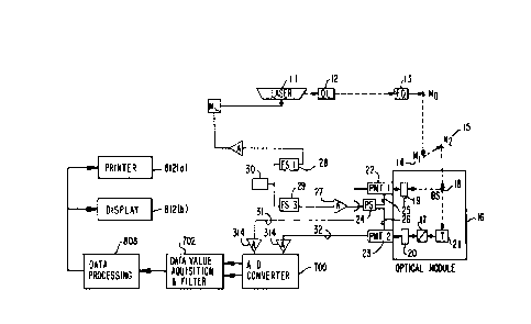
illustrated in Figure 1, laser 11 is a mode locked Nd-YAG laser
which synchronously pumps a cavity dumped dye laser 12 *(Antares
model, 765-700 Coherent). The pulse train output is frequency
doubled to W light by using a frequency doubler 13, Coherent
model 7049.
This laser system can cover the wavelength range from
265 nm to 850 nm by changing the laser dyes and the doubler
crystal. The repetition frequency of the laser is normally set
from 1 to 2.00 MHz. All harmonics of the basic frequency can be
used up to about 1000 MHz, (a limit imposed by present
synthesizers and radiofrequency amplifiers). If a lower
modulation frequency is required, the cavity dumper can be set
to any submultiple of 1 MHz, up to a single pulse operation.
The polarization of the dye laser light is vertical
relative to the laboratory axis while the W output from the
doubler 13 is horizontally polarized. The plane of polarization
of the W beam is rotated to 35 degrees from the vertical (the
ideal polarization angle for lifetime measurements) using an
arrangement of two mirrors. The mirrors 14,15 which not only
change the polarization angle of the exciting light but also
steer the beam into the optical module 16, and have a metallic
coating (Melles Griot coating 028); since a dielectric coating
would give rise to a wavelength and polarization dependent
reflection. The emission of the sample may be polarized by
polarizer 17 for measurement and study of anisotropic decay. The
*Trade mark
-
X'``
1 3361 39
- 18 -
optical module 16 also includes a quartz beam splitter 18, filter
holders 19,20 and a sample receiving holder 21.
*Hammamatsu R928 photomultiplier tubes 22,23 are
selected because of their wide-range wavelength sensitivity, high
gain, low price and relatively small color effect.
The modulation of the PMT tubes 22,23 is obtained by
application of an alternating voltage to the second dynode D2
through a power splitter 24, as illustrated at 25,26. The
characteristic curve of the PMT has a sharp rise, then the
current reaches a maximum and decays again as the absolute
voltage of the dynode increases. In order to modulate the gain
of the PMT an RF voltage of about 40V peak to peak is needed
corresponding to an average power of 4W on a 50 ohm terminator.
The RF voltage is provided by an RF amplifier 27 (*ENI Model
603L).
Instead of attempting to acquire the entire frequency
range in one measurement, we acquire the range from 1 MHz to 500
MHz in three steps. The laser is mode locked at F1 by frequency
synthesizer 28, while the PMT's are pulsed at F1 + 40 Hz, 40 Hz
is the cross correlation frequency by frequency synthesizer 29.
The synthesizers 28,29 are maintained in a phase locked loop
figuratively illustrated at 30. In normal operation, the
synthesizer 28, is set at a frequency of 1 MHz with a pulse width
of 100 ns. Synthesizer 29 is set at 1 MHz + 40 Hz. The pulse
width is 100 ns.
The duty cycle becomes 1/10 with a reduction of only
a factor of 5 with respect to the stAn~rd single frequency
mixing (duty cycle ~). Using this pulsed cross-correlation
signal, about nine different frequencies can be easily collected
in the range from 1 to 9 MHz. Then, the base frequency of the
synthesizers are set at 10 MHz, and 10 MHz + 40 Hz with a pulse
*Trade mark
xi
' -
1 3361 39
-- 19 --
width of lO ns and the duty cycle is still 1/10. Again,
frequencies are collected in the range from 10 to 90 MHz.
Finally, the base frequency of the synthesizers are set at 100
MHz and 100 MHz + 40 Hz and the pulse width to about 2 ns and
frequencies are collected from 100 MHz up to about 250 MHz. This
frequency limit is imposed by the PMT detectors and by the
fluoresce~c~ characteristic of the emitting substance. The
reduction in acquisition time with respect to the prior art
sequential multi-frequency mode is about a factor of ten, since
ten frequencies are collected simultaneously.
The output of PMT tubes 22,23 carry the phase and
modulation information imparted by the sample on a correlation
frequency of 40 Hz. The cross-correlation current signal on
signal lines 31,32 is first converted to a voltage signal, and
then amplified by amplifiers 314, as more fully explained with
respect to Figure 3. The amplified signals are then digitized
at 700, as hereinafter explained.
In the digital acquisition system of our invention,
most of the analog electronics have been eliminated. The only
analog elements used are the current-to-voltage converters 300
needed to transform the output of the photomultiplier tubes to
a voltage and the amplifiers 314, to boost the signal level. The
current-to-voltage converter and amplifier are built directly
into the empty slot of a commercially available data acquisition
board. In one embodiment of the invention, a *"MicroWay A2D-160
board was used because of its speed, its two collection channels,
and its use of the computer's direct memory access (DMA)
capabilities. This board fits into a slot of any *IBM-PC-
compatible computer. Direct memory access relieves the central
processing unit (CPU) from processing data during
*Trade mark
X~
-- 1 3361 39
-
l the acquisition period, so that data collection and storage
occur in the background. Therefore, the CPU is used only for
the digital filtering processes and determination of the
phase and modulation values of previously acquired waveforms.
The CPU is free most of the time to run normal "housekeeping"
tasks, such as displaying information on the status of the
instrument. The A2D-160 board has a 12-bit analog-to-digital
converter with a maximum sampling rate in single channel mode
of 160 KHz. In our experience, 12-bits were al~ays
sufficient to obtain good accuracy. The actual resolution is
improved due to the noise level of our signal. We have
estimated that in our experimental condition we have about
15- to 16-bit effective reso~htion. With respect to the
sampling rate, we are ~7ell below the board's limits. For the
measurements reported here, we have used a sampling rate of
2.56 KHz.
Referring now to ~igure 3 the analog circuitry is
illustrated in schematic form. The output signals of the
photomultiplier tubes enter the current-to-voltage converter
300 through a 50 ohm resistor 302 and a 1 megaohm resistor
304 to ground combination. The signal continues through this
combination to an active low pass fiiter comprised of an
operational amplifier 306 with a negative feedback path
comprised of a parallel combination of a 1 megaohm resistor
308 and a 1000 picoforad capacitor 310, the effect of which
is to attenuate higher fre~uency signals. The operational
amplifier is powered by a positive 12 volt signal 301 and a
negative 12 volt signal 303. A variable 10 kilo-ohm resistor
312 is used to adjust the zero offset of the operational
amplifier 306. The operational amplifier 306 used is an
ADS15 manufactured by Analog Devices, Inc.
` - -21-~
1 3361 39
l The output of the current-to-voltase converter 300
is then directed to a variable gain amplifier 314. The
variable gain amplifier 314 is capable of amplifying the
output of ~he currcnt-to-voltage converter 300 by a magnitude
of 1, 10, 100 or 1000 times. The variable gain ~mplifier 314
is powered by a positive 12 ~olt signal 305 and a nesative 12
volt signal 307. Adjustments to the variable gain ampli~ier
314 are made through a pair of 10 kilo-ohm resistors 316 and
318 which are connected to the positive and negative 12 volt
signals and to ground through a pair of 1 microforad
capacitors 320 and 322. The value of the gain on .he
variable gain amplifier 314 is determined by z signal
generated by a bank of relay~-324.
The ban~ of relays-is comprised of three
independent relays 326, 328 and 330. The relays 326, 328 and
330 are controlled by digital logic circuitry comprised of
three integrated circuits 332, 334 and 336. Each relay 326,
328 and 330 is comprised of a set of diodes 321, 323 and 325
a set of coils 327, 329 and 331 and a set of switches 333,
335 and 337. One side of each diode 321, 323 or 325 is
connected to a positive 5 volt source 339 while the other
side is connected to a digital integrated circuit 334 via
lines 341, 343 and 345. When the value of any of the three
outputs of integrated circuit 334 are logic 0, which
corresponds to 0 volts, then that particular diode 326, 328
or 330 conducts current and magnetizes the particular coil
327, 329, 331 and thereby closes switches 333, 335 or 337.
The digital circuitry comprised of three integrated
circuits 332, 334 and 336 control the gain on amplifier 314
by controlling the relays 326, 328 and 330. Integrated
circuit 332 is a series of four NAND gates 338, 340, 342 and
344 which receive ~n I/O SELECT and I/O WRITE signal from the
1 3361 39
- 22 -
host computer. These two signals are used to latch the
integrated circuit 336. Integrated circuit 336 receives three
input signals D0, Dl and D2 from the host computer. These three
signals are latched and stored in the integrated circuit 336 and
are ou~ to three inverters 346, 348 and 350 which are realizéd
on one integrated circuit 334. By varying the possible
combinations of D0, Dl and D2, the gain on the variable gain
amplifier 314 can be altered. Table 1 given below contains the
combinations of D0, Dl and D2 and the gains they cause to be
made.
- GAIN TABLE
D2 Dl DO GAIN
0 10
1 0 1 100
0 1 1 1000
In the digital acquisition system of the present
invention, the host or controlling program is an adaptation of
the standard acquisition software used in our laboratory and is
available through Globals Unlimited, Department of Physics, UIUC.
The program starts by initializing the hardware and setting up
data files. First, the analog-to-digital board is disabled and
the on-board timer is programmed. The A2D-160 card has a 4 MHz
clock which is used by an AM9513 counter chip from Advanced Micro
Devices. A "master reset" is issued to the AM9513, this resets
and stops all counters; counter one is then loaded. This counter
divides the 4 MHz clock to provide the appropriate sampling rate
for the cross-correlated signal, which we have chosen to be at
40 Hz. Next, the DMA channel 1 of the *IBM PC is
*Trade mark
-
X~ .
`~ -- - -23-
.
1 3361 39
1 masked, and programmed to transfer 2560 data points from the
analog-to-digital card to a storage vector in the m2in
computer memory. The 2560 data points represent 1280 data
points per channel, which correspond to 32 data points per
5 period for 40 periods. The 32-data points-per-period was
chosen because the highest harmonic that the f2st fourier
transform (FFT) algorithm, used by the filtering routine, can
resolve is equal to half of the number of data points. The
-possibility to analyze up to the si~:teenth harmonic was felt
to be high enough for our application. This is not a
limitation, because the number of dzta points per period can
be increased with only a linear pen21ty of computztion speed.
The 40-period integration range was chosen because at the
cross-correlation frequency of 40 Hz used in our instrument,
data are collected in one second, and also for the efficiency
of the ~iltering, which will be discussed later. Channel 3
on the PC interrupt controller is masked, and a new interrupt
vector, pointing to a display and save routine, is loaded.
~hen the timer, the DMA, and the interrupt controller have
been programmed, the DMA and interrupt controller are
unmasked, and the timer is started. The timer is
free-running, so data are collected asynchronously.
The data collection proceeds, simultaneously
converting b~th the excitation and emission channels by using
the two independent sample-and-hold circuits, and is sampled
by the 12-bit analog-to-digital converter with a full scale
range of -5 to +5 volts. As illustrated in Figure 7, at the
end of the conversion process the DMA 702 is addressed. The
DMA then transfers the output of the analog-to-digital
converter into the main memory of the computer as illustrated
at 704; then the other sample-and-hold circuit is read,
converted, and stored. The whole cycle is repeated until the
-
-
~ 24- ~
1 336 1 39
1 2560 data points are coll~cted. Once the data has been
stored, the DMA generates an end-of-process which triggers
the interrupt routine indicated at 706. The interrupt
routine 706 folds the 40 periods that arise from the one
second integration into one, and then reduces the 32 data
points into four bins, representing four phzses o. a period
at the lowest harmonic fre~uency. The DC, AC, modulation,
and phase of the waveform can be rapidly calculated from the
values of the four bins. Those values are used only to give
basic information "on the fly" for the data being collected.
This information is displayed at the top line of the computer
screen, and is updated every second. This information is
useful to the user for conti;nuous monitoring of the measuring
~ conditions of the instrumen~: The interrupt routine
reprograms the DMA and the~interrupt controller and restarts
the counter. The cycle starts again and is continuously
repeated.
At the beginning of a measurement, the program sets
the basic frequency of the synthesizer and asks for the
reference lifetime value. A dark waveform is then digitized
by repeating the interrupt cycle ten times. After the data
have been collected, the averaged and folded waveform is
analyzed by a FFT routine which provides additional
filtering. ~he real and imaginary parts of the FFT are
sufficient to calculate the AC, DC phase and modulation of up
to the sixteenth harmonic. These values are subtracted from
the sample and reference waveforms to reduce in-phase pickup
noise. After the dark waveform is measured, the sample is
illuminated and the fluorescence signal is acquired. The ~.C,
DC, phase and modulation values are determined at the same
moment. The reference compound (lifetime = ref) is then
illuminated, and its AC, DC, phase and modulation values are
~ 25- -~
- ` 1 3361 39
1 calculated. When both the sample and reference have been
collected, absolute phase and modulation values are
calculated using the following expressions.
M MYam
Mref ~1~ ~2t f2
L.~d
~corr = tan~ red + (Psam ~ ~rer)-
The sample is again illuminated, and its modulatioi. and phase
values are determined. Absolute phase and mod~la,ion values
are then calculated using the new values of the sam?le
modulation and phase and old reference numb rs. Tne
corrected modulation and phase numbers are zveraged together,
and the standard deviation is calculated. The rererence
sam~le is then illuminated and the cycle is repeated until
the variance is below 0.2 degree and 0.004 for the phase and
modulation, respectively.
This entire process is automatically controlled by
the on-line computer using the Globals Unlimited software
described above, as driven by the executive level software
described in Figure 8, and attached hereto as Appendix ~.
Referring to Figure 8, the entire procedure is
shown in flow chart format. The data collection as described
above is shown by block 802 of the flow chart. After the
collection of data, the software checks to see if the EOP
interrupt has been received thus indicating that the data is
.
ready. This is represented by block 804 and corresponds to
line 11 through line 40 on page 3 of the computer program
listing as set forth in Appendix A. If the interrupt has
been detected, the CPU transfers control to the interrupt
-~6-
~, . ,
1 3361 39
l routine indicated by the dotted box 803. The first box 806
represents the portion of the interrupt software that is
responsible for folding the ac~uired waveform into one period
of time, the reasons for this are explained earlier. The
software that corresponds to box 806 is given in line 45 on
page 3 of the computer program listing throush line 2 on page
4 of the computer program listing. Bloc~ 808 represents the
portion of software responsible for calculating the discrete
fourier transform of the collected waveform. The software
corresponding to box 808 is given in line 60 on page 10 of
the computer program listing through line 60 on page 11 of
the computer program listing. Block 810 represents the
portion of the software that1is used to calculate the DC, AC,
modulation and phase of the wave form. The software
corresponding to box 810 is given in line 65 on page 11 of
the computer program listing through line 36 on page 12 of
the computer program listing. Block 812 is a routine that
displays the information calculated in block 810. The
software corresponding to box 812 is given in line 20 on page
4 of the computer program listing through line 20 on page 5
of the computer program listing. The information is
displayed at the top line of the computer screen, and is
updated every second. Block 814 represents the software used
to reprogram.the DMA 702 shown in Figure 7, the interrupt
controls and it also restarts the internal counter. The
software corresponding to box 814 is given in line 25 on page
5 of the computer program listing through line 20 on page 10
of the computer program listing. Upon completion of the
routine described in box 814, the software is now returned to
the main software routine. Block 816 copies the information
calculated by block 810 into new variables for further
manipulation.
~, -27-
1 336 1 39
l Whcn both the sample and reference waveforms have
been collected as described above, absolute phase and
modulation values are calculated, ~Jhich is represented by
block 818. The corrected modulation and phase num~ers are
averaged together to form average values as is shown in block
820. The processing corresponding to boxes 816, 818 and 820
is done in a software loop given in line 60 on page 12 of the
computer program listing through line 59 on p2ge 13 of the
computer program listing. After averaging the values
together, the standard deviation is calculated and checked to
see if it is in the specified range as shown in decision box
822. If standard deviation is not acceptable, the process of
analyzing the data is repeateid. If standard deviation is
- within tolerance, the software returns to its starting point,
illustrated by block 824. The calculation of the s.andzrd
deviation and the software corresponding to decision box 822
is given in line 61 on page 13 of the computer program
listing through line 15 on page 14 of the computer program
listing.
The digital acquisition system of the present
invention excels at filtering. This operation must reject
random and harmonic noise. Simulations show that if the
second harmonic has an amplitude of 0.05 of the fundamental
after the filtering, and is incorrectly associated with the
first harmonic, the resulting phase measurement can be off by
as much as five degrees. This is a very large error, and
therefore the harmonics must be reduced to less than one part
in 200 for the effect to be less than 0.2 degrees. In the
st~n~rd analog electronics of most commercial frequency
domain fluorometers, six pole active filters are used to
perform the appropriate filtering. These filters are hard to
tune, suffer therma~ drifting problems, and have
~ -28-
s 1 33 6 1 3 9
1 amplitude-dependent phase shifts, which become a problem if
the sample and reference compounds do not emit nearly equal
amounts of light. If this is the czse, then the signal out
of the PlIT will have different am~litudes for the sample and
reference cuvettes and the resulting phase-shifts from the
filters will introduce a systematic phase deviation. The
digital acquisition system of the present invention uses a
sequence of two digital filters that do not suffer rom these
problems.
The first digital filter is the averaging filter.
Since data are collected by acquiring 40 periods in a
continuous stream and folding into one period, any freq~ency
that is not a harmonic of thé fundamental will destructively
interfcre with itself. Also, all signals which are not
synchronous with the fundamental will average out. For
example, if ~he fundamental is at 40 Hz and a 20 Hz signal is
added, then in one 40 Hz waveform there is one-half of the 20
Hz waveform and the next 40 Hz waveform will contain the
opposite hal~ of the 20 Hz waveform. When the two waveforms
are folded and added, the 20 Hz signal will cancel out
exactly and the 40 Hz signal will remain. The filtering
action of this filter depends on the number of waveforms
collected and folded. The experimental filter response of
our 40 waveform-averaging filter is shown in figure lOa. The
points for this figure were obtained by applying a sinusoidal
signal out of a HP3525 synthesizer directly to the A2D-160
board and then varying the fre~uency over the range specified
in the Figure.
An inherent property and, as we show later, an
advantage of the averaging filter is that it lets the
harmonics pass through. To separate the fundamental and the
harmonic information, the averaging filter's output is
~_ 29
1 336 1 39
1 processed by a FFT routine; The FFT routine also acts as a
filter, because it resolves the input waveform to a DC value,
thc fundamental frequency, and its harmonics. Therefore, any
of the harmonic frequencies can be rejected by simply
ignoring its output from the ~FT. The e~?erimental filter
response of the FFT, retaini~g the fundamental fre~uency
only, is shown in ~igure lOb. The same signal as in Figure
lOa was used to obtain the e~perimental points in Figure lOb.
The FFT also provides the values needed to calculate the
phase and modulation of the acquired wave orm. The two
filters, the averaging and the FFT, are in series and the
final result is the product of the two filters. The total
filter response, for the fun~amental, is shown in Figure lOc.
As can be seen, the harmonic~ are rejected by more than a
factor of 2,000. This is an improvement over the analog
electronics of about a factor of ten.
To illustrate the advantages of the digital filter
over the analog electronics, we used both methods to perform
a series of measurements of phase and modulation values as a
function of the amplitude of an input signal. The input
signal was composed of a basic fre~uency of 40 Hz plus a
uniform noise band limited to 1000 Hz of 100 mV amplitude.
The signal at 40 Hz was varied in amplitude while the noise
level was lef.~ constant. The phase of the reference with
respect to the sample channel was 180 to avoid the
indeterminate region of the 0 to 360 for the analog
acquisition mode, which would introduce additional phase
noise. Above 1 V signal, both methods provided an adequate
response: the average deviation and the standard deviation
of the phase value were within 0.1, a value commonly
considered adequate for frequency domain fluorometry. When
the signal-to-noise ratio became smaller, the performance of
1 336 1 39
- 30 -
the digital acquisition system was clearly superior to the analog
electronics. The experimental conditions used in this test were
typical of most of the measurements in frequency domain
fluorometry where the signal-to-noise ratio is generally about
ten.
A typical measurement from the fluorometer of the
present invention is shown in Figure 9. The phase and modulation
values for a solution of P-terphenyl in alcohol are shown
together with the best fit for a single exponential decay. The
excitation source is a mode-locked Nd-YAG laser which
synchronously pumps a dye laser (*Antares model, Coherent, Palo
Alto, California). The output of the dye laser is cavity dumped
and doubled to obtain ultraviolet (W) light pulses. This pulse
repetition rate is exactly 2.00 MHz. The quality of the data
acquired in parallel, using a 10 second integration time for each
of the three base frequency acquisition modes is better than the
data obtained by the standard sequential mode using the analog
electronic acquisition and 10 seconds integration time for each
point. Note that with the parallel mode the entire decay was
acquired in 60 seconds, as compared with 540 seconds effective
integration time for the normal sequential mode. The actual
acquisition time in the normal sequential mode was much larger
(about 1000 seconds) due to the overhead time in manually setting
the synthesizers to each new frequency and the need to acquire
a dark current reading for every frequency.
The digital acquisition method described with respect
to this invention allows for much better signal filtering than
the analog electronics currently used in freguency domain
fluorometers and also provides for the added
*Trade mark
X!
3 1 -- ~ ~ ~
1 336 1 39
l capability of parallel frequency acquisition. Another
advantage of the digital electronics is the intrinsic
capability to modify the base filter frequency by simply
entering into the co~puter a different number for the
acquisition period.- Using this possibilitY, we have been
able to determine the best cross-correlation fre~uency to be
used on the basis of the phase noise characteristic of the
synthesizer.
Figure 2 illustrates the parallel phase fluorometer
of the present invention with a different detection and cross
correlation means. As illustrated in Figure 2, the light
source is a mode locked in Nd-YAG laser ~0 which
synchronously pumps a cavit~ dumped dyelaser 51 in a manner
similar to that illustratëd previously with respect to Figure
1. The pulse train out is frequency dou~led to UV-light by
using a frequency doubler 52. Lasers 50, 51 are driven by
mode lock driver 53 and cavity dump driver 54 which are in
turn driven by a radio frequency amplifier ~5. Frequency
synthesizer 56 provides the driving frequency for the pulsed
light source, while frequency synthesizer 57 provides the
driving frequency for the cross correlation means. Frequency
synthesizers 56 and 57 are phase locked with a phase lock
loop with frequency synthesizer 56 generating a first
predetermined fundamental frequency f1, and frequency
synthesizer 57 generating a second frequency, which includes
fl +fc wherein fc is a correlation frequency. While fl is
selected to insure a high number of intrinsic harmonics, fc
is selected primarily for compatibility with the ~rray
detector as will be hereinafter further discussed.
The polarization of the dyelaser light is vertical
relative to the laboratory axis while the W output from the
~_ -32-
1 336 1 39
1 doubler 52 is horizontally p~larized. The plane of
polarization of the W beam is rotated to 35 degrees from the
vertical (the ideal polarization angle for lifetime
measuremcn~s) using an arrangement of two mirrors, 58, 59,
5 which not only change the polarization angle of the exciting
light, but also steer the beam into the optical moGule 60.
The mirrors 58, 59 have a metallic coating since a dielectric
coating would give rise to wavelength and polarization
dependent reflection. The pulsed light beam is spli_ by beam
10 splitter 61 into a reference beam 62 and a sample bezm 63.
The sample beam 63 impinges on a ~ample contained in sample
holder 64 and the scattered light is passed through an
aberration corrected polychromator 65 to the array detection
- system. The reference beam 6~ is directed to a sca tering
15 surface 66, the output of which is measured by a re_erence
detector 67 ~Jhich may be a photomultiplier tube 2S was
previously described with respect to Figure 1. The
photomultiplier 67 mixes the output of RF amplifier 68 and
the si~n 1 generated by reference beam 62 to derive a
20 reference signal on signal line 69 which is essentially the
correlation signal plus any system noise or deviation not
related to the sample. The array det~ctor will be more fully
described with respect to Figure 4, it is comprised of three
principle parts, image intensifier 70 a phosphorous layer 71
25 and a semiconductor array detector 72. In the embodiment
illustrated in Figure 2, the array detector was an Optical
Multichannel Analyzer, Princeton Instruments, model
IRY-512g/rb with an ISIT gatable proximity~focused
micro-channel plate (MCP) image intensifier, that is
30 optically coupled to a diode array.
The array detector 72 provides a sequential analog
output on signal line 73 at a preselected frequency, varying
from 30 to 120 sweeps per second. The image intensifier 70
..
~ 33-
` 1 3361 39
1 is normally used to increase the gain of the array detector
72. However, as used in the present invention, the biasing
networ~ for the image intensifier normally holds the
photocathode potential at appro~imately 180 to 200 volts more
negative than that of the potential of the microchannel
electron intcnsifier 70. As driven by radio frequency
amplifier 68, however, the cathode is driven to a g2ted mode
wherein it is approximately 20 to 40 volts more positive than
.the image intensifier and effectively acts as a g2.e to
prevent the light from the sample from reaching the array
detector 72. The cathode in front of the image intensifier
is gated closed at a rate fl + fc determined by radio
frequency amplifier 68 and f~equency synthesizer 57. The
~~ sample is excited at frequency f~ by sample beam 63 and the
emission spectrum from the sample is also varying at a
frequency fl, with certain phase and modulation relationship
with respect to the excitation. The e~ission spectrum at f1,
and the optical gating of the image intensifier at fl + fc
creates two optical frequencies corresponding to the sum and
difference of fl and fc. Since fc is selected to be
relatively low, on the order of 15 Hz, a signal at this
frequency is received by the array detector 72. A sweep rate
of 120 sweeps per second of the array detector results in a
8X sampling pf the 15 hertz correlation frequency imposed on
the array detector 72 by the optical cross correlation of the
image intensifier 70. Each complete cycle of the correlation
frequency at 15 hertz carries the complete phase and
modulation information imparted by the sample to the sample
beam 63 by the emission characteristics of the sample.
The operation of the analog to digital converter,
the data value acquisition programs, the averaging filter and
the fast fourier transforms are essentially identical to that
~ 1 3361 39
1 described for Figure 1, with exception of the averaging or
folding period. The differences relate to the differences in
the filtering and avcraging as necessary to accommodate the
shift from 40 hertz to 15 hertz in the folding and averaging
steps.
Figure 4 illustrates in a more figurative manner,
the array detector illustr2ted at 70-72 in Figure 2. As
illustrated in Figure 4, the device includes a quartz or
optical fiber window 75, a photocathode 76 driven by input
line lead 77, a microchannel plate electron intensifier 78
which is nominzlly biased with in znd out leads 79, 80. The
array detector also includes phosphor lzyer 81 positioned
between the image intensifier and the diode array 82. The
~- phosphor layer and the diode array are coupled by means of an
optical fiber coupler 83. The diode arrzy 82 is z standard
diode Reticon~l detector and array by Princeton Instruments
The bizsing network for the array detector
illustrated in Figure 4 is illustrated in ~igure 5 wherein a
high voltage intensifier bias is imposed at 84. The -6.8KV
is supplied by a po~er supply, not shown in Figure 2, to the
cathode through a series of high resistances. The resistors,
nct shown, are for current limiting. The dc signal path from
the cathode ~not through any capacitors) goes right through
to D1 and D2. The purpose of D1 and D2 is to accelerate the
electrons to the grid. It is important to note that this
device is never really turned off. This ~ill be explained
shortly. The RF signal from amplifier 68 is inserted at 85
and the photocathode is biased as indicated at 77. The
change produced by the incoming RF on the gain of the image
intensifier through the acceleration voltage provides the
modulation of the optical signal. The circuit illustrated in
Figure ~ is an adap~ation of the original circuit provided by
3 ~
1 336 1 39
1 Princeton Instruments with the optical Multichannel Analyzer.
~cnor diode 86 is added to bias the photocathode 76 to the
middle of the OMA gain curve as illustrated in Figure 6.
Diode 86 is used to modify the voltage bet~een the cathode
and the MCP. The value of this diode is chosen in order to
alter the gain by approY.imately a factor of 2. By reducing
the yain by a factor of 2, the electrons are accelerated at a
much lotJer rate in operation, the dynamic range of the O~
.utilized is from approximately 40 indicated at A to 180
indicated at A' in Figure 6. The use oI a 90 volt zenor
diode 86 provides a biasing voltage and an ~C peak-to-peak
voltage of approximztely 60 volts as in~icated by B-B' in
Figure 6. As indicated previously, the photocathode
`; potential on line 77 is normzlly set by the biasing circuit
to be approximately 180 to 200 volts more negative than the
potential of the microchannel plate 78. By biasing the
photocathode with zener diode 86, the excursions of the radio
frequency input signal at 85 raise the potential of the
photocathode to approximately 20 to 40 volts more positive
than that of the image intensifier 78, thereby effectively
gating the image intensifier and preventing any of the
emissions from sample in sample holder 64 from reaching
either the phosphor layer 81 or the diode array 82.
All capacitors, except for the two coming in at the
RF input are used for stability purposes. The average value
of the cathode voltage should not change; therefore, the
capacitors are used to stabilize this average value.
The remaining two capacitors, decoupling capacitors
are to prevent the -6.8KV cathode voltage from leaking into
the RF signal.
The use of the array detector, as illustrated in
Figure 2, enables t~he separation of emission spectrum in at
~ 3~- ~
1 336 1 39
1 least two different ways. First, the emissions may be
separated by thcir spcctral content since the OMA is
connected by the polychromator 65, and the xy location of the
emission can be tagged with the spectral response. ~urther,
5 by combining the x,y coordinate informàtion with the time
resolved information, multicimensional informi2tion a~out a
specific spectrum may be calculated. This information can
subsequently be combined with the phase and modulation
information derived by the processing means from the fast
10 fourier transform to further assist in the separation of
characteri5tic emissions in a mixed or multicomponent media.
3o
3 ?17 ;~3 J~?~ UIUC IIE;`G
A~lDIx `A'
.~t d~_e32pi 1 3 3 6 1 3 9
AA~AAlA~A~ A~ AAJ~ A~ A~lAlAA~ AA~AJ~ A~AJ~ AA~
P a r a 1 l e l I n c e r n a 1 T r i g g e r D r i v e r
llects 32 data poLnt~ using the internal trigger generatsd by
the first count~r of the 9513.
J~AAlJ~A~.AA~ AAAAl~ lAl~AAAllAl~ AA~ A~ A~ A~A~A~A~)
terface
Us~
cr~nQ~globvarp~mathutil~ioutillp;
const
ndpfc - 256; ~ number of da;a points per waveform for data collection~pof2fc e 8; ( power of two needed for d~ta collection )
ndpfm - ndpfc div 4; ( number of data point~ per wa~efDrm for monitoring)
pof2fm - pof2fc-2; ( power of two needed for mon{ toring ~
nwfc - 40; l number of waveforms or data collection )
nwfm = lO; ~ number of w~veforms for moni~orlng )
counc - ndpfc*nwfc+l; ( number of data point~ eo collect}
~trpeharm : Lnte~er-l;
ma~ rm = ndpfc div 2;
type
darray-ar~ay[0..2*countl of integer;
rarray-arrayLO..ndpfc3 of single;
var
dataptr : ^tarr~y;
cha,chb,zero : rarray;
oldvector : pointer;
div_rate,divfc,divf~ : word;
strtcnt,strtcntfc,s~rtcn~fm : word;
endcnt,endcntfc,endcntfm : word;-
segcnt,segcntfc,segcntfm : word;
ndpts : word;
pof2 : byte;
procedure setup;
proce~ure arm;
procedure ~nitpor~;
procedure initinterrupt;
procedure delnltinterrupt;
procedure tri~8er;
procedure gain sa~;
procedure gaLn ref;
procedure ~hmod(xr,xi : rArrsy; var phl,ph2,acl,ac2 : mult; ~ar dcl,dc2 : ~in~le~;
procedure ~er.pt(var phl,mdl,acl : ~ult var dcl : 6ingle; timeC : integer);
procedure d~rk;
procedure SAMPLE;
procedure R~FER~NCE
~le~entation
~ .
us~s ~
~'io~tilp;
X3
~ . .
1 3 3 6 1 3 9
motor _ O;
base ~ '3eO; Icard base address)
cdata ~ 3eO; [g513 data r~gister3
_cntrl ~ '3e~; ~9513 eontrol register~
_,cereg - 3e2; (adc board concrol reglster~
aml - S3e6; (anslog module one - sampl~3
am2 - 3~8; (analog modula two - reference)
endm~ - 'Oa; (d~a write single m~sk re~iscer)m~kdma - Oa;
~ r ~ Ob; ~dma wrlte ~ode register)
clearff - 'Oc; Idma cle~r ff regis~er)
page - 83; ~ ~na separ~te page register ch~
ddr - 02; ~dma addre~s chn ~2)
dmaword - $03; (dma word chn ~2)
nseoi ~ $20; (interrupt controller )
~skint - '21;
enlnt - '' 2 ~;
intn _ ~;
chn - l;
ictreg - $e4
Ixxxx xxOO ~1~ perlod -1023)
(xxxx xlxx mls gen~rator
(xxxx Oxxx tri8~er internall
~xxlO xxxx op ~ode si~ultan~ous S/Hl
lccxx xxxx comand bits)
lpage : word-O;
opage : wordsO;
daseg : word=O;
dsofs : word-O;
osegcnt : word-O;
phas~ : sin~le~O;
mde~ : s~ngle-l;
dce~ : single-O;
mdex : single-l;
dcsx : slngle-O;
sttrex : word~$7000;
attrem : word-$7000;
i ~ :srray~0..80] of integer-(
'OfOO,
Of~4,$0f~3, Of3a,$0f20,$0f20,$0f20,$0f20,$0f20,`0f20,"0f2Q,
Of41,$0fS3, Of3a,$0f20,$0f20,~Of20,$0f20,$0f20, Of20,'Of20,
`Of4d,SOfS3, Of3s,~0f20,$0f20,~0f20,$0f20,~0f20, Of20, Of20,
Oi-20,$0f20, Of20,
"Of44,$0f~2,"Of3a,$0f20,$0f20,$0f20,$0f20,S0f20,$0f20,$0f20,
S0f41, ~OfS2~ of3~$0f20~SOf20~SOf2Q~sof2o~$0f20~$0f20~$0f20~
$0f4d, Of52,~0f3a,$0f20,$0f20,$0f20,$0f20,$0f20,$0f20,$0f20,
$0f20,'0f20,'0f20,
SOf;O~ Of48~ Of41~$0f53~$0f45~$0f3s~5020~$0f20~$0f20~$0f20,$0f20
$0f20,$0f20,$0f20);
1 1 : integer -0;
~ lnceger -0;
i k : integer -0;
i_tr : ~lngle-O;
i st : stri~g~8]=' ~;
fold : byte-40;
type
v~cndp - arrayLl, (ndpfc dlv 2)] of ~lngle;
~ o~! ~
I_
3 U i U C h E r ~
var f~'
dark AC,da~ ph : mult;
aux,dark_dc : single;
phem : mult;
phex : mult;
acem : mult;
acex : ~ult;
rfold : single;
dummy : po inter;
procedure ~ntdriver
interrupc;
b~gin
., . . . _
AA*~AAAAA~l~llAlAlAlAlllAllAAlllAlAllllAlllAAlA~lllAAlllAllAAAllAAAlAAlAAAAJlA
Was the EOP interrupt gonerated by D.~A channel 27
AlAAAA,-AAAAAAAAAAAA.lAlllA~AAAAlAA~AA~A~A~*AAA~AAA*A**A~AAAlAAAAAAlAAAAA,ll.~l)
portt$8~;
~f (i_i and ~l shl chn) - (l shl chn)) then
begin
dec(segcnt);
7~A`~*AAAAA~AAAAAlAlAAA~lAAAAAAllAAAA~AA~AAAA*AAA*AA*AAA~A~AAAA~lllAAlAAAlAAA~l~A
Has all of the data been collected?
AlAAAA.~Ai.~A:tA*A~AAAA~A~AA~A71:A,~.A~.AAAAAA~ AAX~ lAAilAiAlAAAA~AAA~ *A~AA)
if segcnt<l then
begin
port;_ctreg :-ictreg and $3f; ~clear FIFO and disable DMA ff on board)
pore cnerl ;-$dl; (disarm counters 1,5)
port. cntrl :-$e5; ~clear tog~le 5)
if moto~ o l then
begin
attrex:-$7000;
attrem:-S7000;
*A~ A~AJIllAAAAAA.~lA.lAlAAlAAAAAA~ AAAA~lAAA.llAAAlA~AAllAAlllA-~AA~ **AAAA
fold ~o one period
A~A111AA1A~A~AAA~ A~AAA~A~AA~1AA1A1A1AAAA1~ A~ A~A~ AAAA~AAA1A11)
for i_k: O to ndpts-l do
begin
lf dataptr^[2*i k+21>2040 then
attrem:-$fOOO;
if dataper^ 2*i k~l~>20~0 then
attrex:= fOOO;
i_i:-i k 6h' l;
chali k~:-tat~ptr ~i i+2~/rfold;
chb~i k~: dataptrA[i i+l]~rfold;
end;
for l k:-ndpts to fold*ndpts-l do
begin
if dataptrA[2*l kl2]~2040 t~en
attrem:-$fOOO;
if dataptr^[2*i_k+l]~2040 then
attrsx:-SfQOO;
ij :-i_k mod ndpt6;
1 l:-l k lhl l;
cha[ij ]:-cha~i_J]+dataptr^[i i+2~/rfold;
~?
'X ~
3 21 ~ 3~ 4990 U IUC HEP~
~` - 1 3361 39
chb~ ]:-chb[i_~]+da~apcr^~ 1]/rfold;
~ end;
phmod(cha,chb,phem,phex,acem,~cex,dce~,dcex);
- if dcex O 0 then
mdex:-acex[itrptharm]/dcex
el ~e
mdex~
str (dcex:5;0,1 s~);
for i_~:- 1 to 5 do
i s~ +37] :- ord(i_st[ij ])+attrex;
-~AAAAAAAAAAAAAAAAAAAAAAAAAAAAAAlAAAAAAAilAAAAAAAAAlAAAlAllAlAlllkAAAAAAAlAAAA
display ac excita~ion
AAAAlAllAlAAAAAAlA~AAAAAAAAAAAAAAAAAlAAlllAllAllllAAAAAlAAAAAAAAJeAAAAAAlAlll)
str (acex[itrptharm}:5:0,i st~;
for i~ 1 to 5 do
I_s~L_~+47~ e ord(i st[ij ])+attrex;
AAAAAAAAAAAAAAAAAAAAA~AAAAAlAAlAAAA~AAllllAlllAAlAAAAAAAA~AAAAAAlAAAAlllAAA~AA
displ~y md excitacion
AAlAllAAAAlAAAAAA~lAAlAlllllAAAlAAAAAAAAAlAAAA~AAlAAllAlAlAAAAAAAlAAAAAlAAA)
str (mdex:S:3,i_st)
for iJ : 1 to 5 do
i s~ +S7] :- ord(i_st[l~ ~)+attrex;
if dcem o 0 then
mdem:~cem[itrptharm]~dcem
else
~tem~
phase:-(phem~itrptharm]-phex~Ltrptharml)*180.0~pi;
if p~asB~O then
phase:-phs~e+360,0;
I~AlAlAllAAAAAAlllAlllAAlAAAAAAAAAA*lAAAlAlAlAAAAkAAAAAAA~lelAAAAAAAAAAAAAAAAAA
displ~y DC emission
llAAAAAAAAAAAAAAAAAAAAlAAAAAAlAlAAAlAAAAAAAAAA~AAAlAAAAAAAAAAlAAAAAAAAAAAAAA~
str ~dcem:S:O,i ~e);
for ij :- 1 to 5 do
L_s~iJ +3~ D ord(i st[i_~])+aetrem
AAAAAAAAAAAAAAAAAAAAAAAAAAAAAAAAAAklllAllAlAAAAAAA~AlAAAAlAllAAAllAllAAAAAAAl
display ac e~lsQion
AAAAAAAAAAAlAAAllAAAAAAAAAAAAAlAAAAAAAAAAAlAlAlAAAAAAAAAA~AAAAAAlAAAlAAlAAl)
6tr ~acem[itrptharm1:5:0,L_ct);
for i_~:- 1 to 5 do
i s[i_J+13] :- ord(i ~t[i_~])+~ttre~;
AAAAAAAAAAA-AAAAAAAAAlAAAAAAAAAAAAAAAAAAAAAAAAAAlAAAAAAAlAAAlAAAAAllAlAAAAAA
~ ~ dLspl;Ay md emission
~ X~s ~a
21~ IQQ~ uruc HEPG
1 3361 39
***** ~ ~ AA~IAA~AllAlA~AAAAA~AAAAlAAAAlAAAAAAAAAlAAAA~AA*A~AllAlAAlAl)
str (mdem:5:3,i se);
for i~ 1 to 5 do
~ s~ +23] :- ord(i_st~ ])+attrcm
~AAAAAA~A~A~lAAA*~AAAAAAAAAAAAAAAAAAAAAAAAA~A*~A*AAAAAAAAAAAAA~AAAAAA*~AA
d~splay phase
AAAAlAlAllAAAAAlAAAAAAAlAAAAAAAAlAAlAAAA*AA*AA~AAAAAAAAAAAAAA*AAAA~AAAAAAA~
6tr (phase:6:2,i st);
for i_3:- 1 eO 6 do
i 9[1_~+73~ :~ ord(i st[i_~])+$7000,
~ -~ move~(~_s,ststusline~,l6~3~ rle to~ line).
end;
flag:-l; --
~AAA~AA~AAlAAAAAAAAA~AAlA~ A~*AAAAAAAAAAA~AAAAAAAA*AAAAl~AAA~AAAAA**AAAlA
reprogram the DMA
~lAlA~llAA~ AAAAAAA~A~AAA~AlAA1~AAAl~AA~AAAAAlAAA~A~ A~AAl~A)
if collect then
beg~n
di~ rate:-div~c;
strtcnt:-strtcntfc;
endcnt:-endcncfc;
segcnt:-segcntfc;
ndpt3:-ndpfc;
fold:-nwfc;
riold:-int(nwfc);
pof2:-pof2fc;
end
else
begin
div rate:-dlvfm;
strtcnt:=strtcntf~;
endcnt:-endcntfm;
~ cegcnt:-Qegcntf~;
ndpts:endp~m;
folt:-nwfm;
rfold:-~nt( nwfm );
pof2:-pof2f~;
end;
ip~ge:=opage;
port~mqkd~a]:-$4+chn; (mask DHA controller)
port m~kintl; (port[mskint~ or (1 shl intn)): (mask interrupt~
port page] :~ipage; (update page reg~sterl
port clearff]:-ipage; (cl~ar D.~A ff~
port d~aaddr]~ (daofs); [losd DMA ~ddress)
port ~m~dr :-hi(daof3);
port d~aword :-lo(strtcnt); ~load DMA counter3
port dmaword.:-hi(s~rtcnt);
port cntrl~:-$09; ~select load ragi~t~r counter 1);
port cdata :=lo(div rate); (load wieh cc~v~rsion rate);
por~ cd~ta :-hL(dLv rate); ( I;
port _ctreg : (lctreg and $3f) or $40; (enable DMA first)
porci ctreg :-(~ctre~ and $3f) or $cO; (enable ~nterruptl
X`~ ~(
~ I .
1 336 1 39
- port mskint]:-(port~mskint] and (not (1 shl intn))); ~un~ask ineerrupt~;
port endma]:-chn; ~ unmask-DMA controller )
~_~ port. cntrl :-''e5; ( clear to~gle 5 )
port[_cntrl :;~'61; 1 load and arm counter 1
port[_cntrl':- 50; [ load coun~er 5 )
port[_cntrl :- 30; - :t arm counter 5 1
end
else
begin
AAAAlAAllAAAAAAAAAAAAAAAAAAAAAA~AAAAAAAAAAAAA**AAA~AAA~AAAAlAAlAAAAAlAAAAAlA
reprogram the DMA tO cross segment boundary
A*AAAAAAAAlAAAlAAAAlAAAllAAlAAlAAAAlAAAAllAAAAAAAklAAAAAAAAAAAA~ lAAlAAlAA)
inc~ipage); l update page register )
port cle~rff]---ipage; I clear DMA ff ]
port;d~aword;:-lo(endcnt); ( load DMA countc~ )
port dmaword ;-h~endcnc);
po~t.l' qA~Ar :-$00; ( load DMA address 1
port dmaaddr]:-$00;
portL page]:-ipage; I update page re~lstcr
port end~a]:-chn; ( unm~sk DMA controller
port ctreg]:-~lctreg ~nd $3f) or $40; (enable DMA first~
port ctreg]:-(ictrc~ ant $3f) or $cO; (enable interrup~
end;
end;
port[$20]:-($60+intn); (speci~ic end of interrupt1
inline($fb); ISTI~
end;
procedure initinterrupt;
be~ln
setintvec~8+intn,@Intdriver);
port[$20}:-($20+inen); (specific end of ineerrupt)
end;
procedure setup;
var
i : longint;
_ begln
ndpts:~ndpfc
pof2:-pof2fc;
port~m~kdma :-$4+chn; (m~sk DMA coneroller)
port[mskint :-port[mskint] or ~1 4hl ~ntn); (mask interrup~3
mark(dummy);
daseg:-~eg(dummy ); lget 20 blt add~o6s)
daofs:-of~(tummy^) + (daseg shl 4);
strtcnt:-4*ndpfc*nwfc+4; ( 2 for two channel~ &
2 bec~use two bytc~ - one word~
AAAAAAAA~i*AAAAAAA~AA*AAAA~AAAlAAAAAAl.~llllAAAAAAAAAAAAAA~AAAAAAAAAA~llAlAlAAk
doe~ ehe DMA cross a segment boundary?
~AAAAAAAAAAAAAAAAAAAAAlAAAAAAAA~AAAAAAAJ~AAAAlAAAAA~AlAAAAAAAlkkAlAA*AAAAAAA)
i:-longint(strtcnt)+longint(dsofs);
If 1>65536 then
: begin
endcnt:-i-65536;
strtcnt -~ trtcnt-endcnt;
getmem(dummy~strtcnt);
.
Z; '17 ~3~ 4~ UIUC HEPG
1 3361 39
~e~d;
n ~ ~dataptr); : ~get memory from heapl
for ~:-0 ~o 2*count do
d~eaptr~[i]: 0: }
daseg: seg(dataptr^[0]); ~get 20 b~t address~
daofs:-ofs(dataptr^[0~) + (d~6eg shl 4);
ipage:-daseg shr 12
opagc:-Lpage;
segcnt~
endcnt:~; ` ~ `=~
strtcnt:-~*ndpfc*nwfc+4; -~ l 2 f~r two ch~nnel~ &
~ 2 be-cause two by~es - one wordl
AA~ AAAAl~AlAAAA~ AA~AA~ AAAAAA~lAA~ AAAlAA~AAAA~A`~ A~ AAA~A
does the DMA cross a segment boundary?
A~ Al~*AAAAlAAlAlAAAlAlAA~AAA~AA~AAAA~AAAAA~AAAlA~ A~A~lAlAA11AAl)
i:-longint(strtcnt)+longint~daofs);
if i>65536 then
begin
segcnt:-2;
endcnt:-i-65536;
sertcnt:-strtcnt-endcnt;
clr.~cr;
gotoxy(2,2);
writeln('sy~tem will cro~s boundary (COLLECTION)');
writ~ln(scrtcnt:6,' ',endcnt:6,' ~);
readln;
end;
segcntfc:-segcnc;
8 trtcntfc:-~trecnt; -
entcntfc: endcnt;
se~cnt~
~ndcnt:-l;
strtcnt:~4*ndpf~*nwfc~4; 12 for two channels &
2 bec~use two bytes - one wordl
.AAAAlAAliAAAAAAAAAAlAAlAil~AAiJ.lJ'll~lAllll~lJ.).l.. lAl~.llA~ A~ A~AA,~A~
does the D.~A cross a segment boundary?
AlA~ A)~ AAA~ A~ A~AJ.~AAAltA~A~Al~AA~A~ lAA~ AlAll~)
i:-longint(strtcnt)+longint(daofs);
if i>65536 then
begin
segcnt:=2;
endcnt~ 65536;
st~tcnt:-strtcnt-endcne;
clrscr;
gotoxy(2,2);
writeln('system will cross bound~ry (MONITOaING)');
writeln~strecnc:6,' ',endcnt:6,' ');
resdln;
end;
segcntfm:=~egcnt;
strtcntf~:-scrtcnt;
endcntfm:-endcnt;
segcnt:-~egcntfc;
strtcnt:-strtcntfc;
endcnt:-endcntfc;
osegcnt:~segcnt;
X~ 3
3 ?1~ 43qi~1 UIUC HE?li
1 336 1 39
port[ ctreg]:-ictreg and S3f; tclear ~I~0 and disablo DMA f on board)
~ar~[dmamodel:_$45; (set DMA mode register
chn 1 x~YYY~nl
wrice xxxx01xx
non-autoinlt
- addr ~ncrom~nt xxOxxxxx
single mode Olxxxxxx~
port'_psge] :~ipags; (updace p~ge register~
' port,clearff':-ip~ge; ~clsar DMA ff)
- -por~,dmaaddr :-lo~daofs); ~load DMA address)
port;. -fld~r :-hi(daof~
port clearff]:-ipage; (clear DMA ~f)
port dmaword]:-lo(strtcnt); ~load DMA word}
port,d~aword]:-hl~str~cnt)-,~ ~~-~- - '~~'~ ~ ~-`~ ''''~~'~ -''' ~'
end;
procedure arm;
begin
port~n~o~]:-~$20+intn); lspecific end of interrupt)
por~[m~kdmal:-$4+chn; (mAsk DMA con~roller~
po~t mskint]:-por~[m~k~nt] or (l ~hl incn); lm~sk in~errup~)
por~.ns~oi]:-~S20lLntn); (Qpecific end of interrupt
port; cntrl]:-$dO; Idlsar~ counter 5)
port _ctreg,:-ictreg ~nd $3f; lclesr FIF0 and disable D.~A~
port, ctreg :-(ictreg ~nd $3f) or $40; (enable DMA firs~)
pQrt[_ctrsg,:-'(lctre~ and $3f) or $cO; (en~bla int~rruptl
po t mskint] :=port[mskint] and ~not ~1 shl in~n~ unmask interrupc);
por~ en~na]:-chn; ~un~sk DMA controilerJ
port cntrl';-$e5; ~clear to~gle 5~
port _cntrl,: `64; (load and arm counter 3)
port,_cntrl :- 61; tload snd arm councer 1)
port;_cntrl':-''S0; (load coun~er S~
port, cntrl;:-'`30; (arm countar 5)
fla~:~;
end;
procedure initport;
var
- ~atetemp : ~(n~le;
begin
por~' cn~rl :-$df; (disar~ all countor~;
port cntrl,:-$ff; (~ast~r reset to 9513~;
port, cntrl,;-Sl7; ~master mode regi3ter};
port[_cda~a :- 0; (set fout eo dl~ by 2);
port[ cdaea :-''2 ; ( ~;
por~ cntrl]:='df; Idig~r~ all couneers~;
port' cntrl :-''l; (Qelect modc regist~r counter 1];
port,_cdata :-$25 ; (mode ~1
port _cdata :~$0b ; (Ra~e Generator with ~BVel Gating)
~act~ve low ~c pulse xxxx xxxx xxxx xlOl
count down xxxx xxxx xxxx Oxxx
bin~ry count xxxx xxxx xxxO xxxx
count repeeLt~vely xxxx xxxx xxlx xxxx
reload from lo~d xxxx xxxx xOxx xxxx
di~able ~peclal ~ate xxxx xxxx ~xxx xxxx
count fl (4.0 Mhz~ xxxx 1011 xxxx xxxx
count on ri~ing edge xxxO xxxx xxxx xxxx
no ~at1n~ OOOx xxxx xxxx xxxxl
if crosscorr 0.0 then
cro~corr:~40.0;
X`~ ~
3 21. .~3~ ~g~13 UIUI~ HEP13
~ 3361 39
~~~eetemp: 84 .0~6/(cro~scorr*ndpfc);
LL~ (ratetemp>65535.0) or (rat~temp<0.0) ehen
begin
div rate:-31~6;
wrlte(#7);write(#7);
put ~tring('~rosscorrelation Frequency Ou~ of Range',23,3,n_video);
put scring('Hit Any Key to Cont~n~e',24,3,n_video);
wait(ch);
end
al~e
div ra~e:-trunc~ratetemp)+l;
divfc:=div rate;
ratetemp:-4.0E6/(crosscorr*ndpfm)
lf (racetemp>65535.0) or (ratetemp~O.O) then
begin
div rato:-3126;
write(~7);write(#7);
put string('Crosscorrelation Frequency Ou~ of Range',23,3,n v~deo);
put strln~('Hlt Any Key to Continue~ ,24,3,n vldeo);
wait~ch~;
ent
else
d~v rate: trunc(ratetemp)+l;
dlvfm:-div_rate;
porc cntrl :-~09; (select load register counter 1);
port, cd~ta;:-lo(div rate); ~losd wi~h conversion rate~;
port, cdata, :-hi(dlv raee`; { );
port cntrl,:- 3; (select mode register counter 3~;
pcrt; cdata]:- Oa; tSelect mode A - Soft-~are-Trlgg~red Strobe)
port, cdata]:- 05; ~w~th No Hardw~re Gating)
ITC eoggle xxxx xxxx xxxx xO10
count up xxxx xxxx xxxx lxxx
binary coune xxxx xxxx xxxO xxxx
count once x-,cxx xxxx xxOx xxxx
reload from load xxxx xxxx x~xx xxxx
disable speclal ~aee xxxx xxxx Oxxx xxxx
count fl ~4.0 Mhz) xxxx 0101 xxxx xxxx
count on rising edge xxxO xxxx xxxx xxxx
no g~ting OOOx xxxx xxxx xxxx)
port cntrl :-~Ob; (3elect load ~egi6ter counter 3};
port, cdata :-$00; (load with zero to clear ~;
port, cdata,:-$00; (dma overflow counter ~; -
-port cntrl,:-"05; Iselect ~ode regi~t~r counter 5);
port, cdata]:- 02; lSelect mot~ A - Soft~are-Triggered Strobe)
port, cdatAl:- Ob; ~with No %ardware Gat~ngl
(TC toggle xxxx xxxx xxxx xOlO
count ~own xxxx xxxx xxxx Oxxx
blnary count xxxx xxxx xxxO xxxx
count onc B XXXX XXXX XXOX XXXX
reload fro~ loat xxxx xxxx xOxx xxxx
di~able speclsl gate xxxx xxxx Oxxx xxxx
coune fl (4.0 Mhz) xxxx 1011 xxxx xxxx
count on rising edge xxxO xxxx xxxx xxxx
no ~aeing OOQx xxxx xxxx xxxx~
port~ cntr~]:- Od; lselect load register counter 5)
portl cdata]:- OO; (load wl~h zero delay)
port[ cdata]:- OO; ~ )
port[ cntrl]: eS; ~cle~r tc coun~er S to dm~ lnhiblt~
end
~5'
3 '' l i' 333 49~13 U I UC HE~G
1 336 1 39
proced~e deinitinter~upt
b~Rin
port ~skdma :-S4lchn; (~a~k DMA controller)
port mskint ~-port~msk~nt] or (1 shl ~ntn); (mask lnterrupt~
port cntrl :-`ff; tmaster reset to ~513);
port cntrl :-~17; lmaster mode register~;
port cntrl :--df; - (t~sarm 811 counters);
port _ctreg :-~ctreg and $3f; (clear FIF0 and disable D~A~
por~ n~eoi]:-($60+intn); ~specific end o~ interruptl
s~tint~ec(8~intn,oldvector)
port~ms~in~ port[mskint] and (not (1 shl lntn)); (unma~k interrupt
port~endma]:-chn; (unmack dma channel~
if d~taptro nil chen
begis ..
d~spose(tatap~r);
dataptr:-nil;
ent;
end;
proce~u~e erigger;
begin
fl~g:-0;
repeat until ~flag-1) or ctrlpres~;
if ctrlpress then
ch:e~27;
end;
proceduro gain sam;
var
g : byte;
begin
gotoxy(1,21);
wrlte('Enter gain : ');
reatln(g);
port~aml~:-g;
end;
.
proc~ture gaLn ref;
vsr
g : byte;
~egin
gotoxy(l,21);
wrlte('~nter gain : ');
rsadln(g);
port[am2]:=8;
end;
procedure phmod(xr,xi : rarray; var phl,ph2,acl,ac2 : mult; var dcl,dc2 : single);
var
ii : integer;
temp,trl,tr2,tll,ti2 : single;
procedure fft(var xr,xi:rarray;nu:integer);
var
n,n2,nul,klI,i,p,kl,kln2 : integ~r;
arg,c,~,cre~l,ci~ag : ~ingle;
function bitr(a,b:integer):integer;
var
jl,j2,i,aux:integer;
_X'~
~ ~ v u i ~
~ begin 1 3 3 6 1 3 9
a;
aux:-O; c --.
fo~ i:-l to b do
. - begln
~2:~ hr 1; ---
aux:~aux*21(~1-2*~2);
~1:-j2;
~nd; ~ --
bitr: -aux;
end; - -
be8in (fft)
n:-l shl nu;
n2:-n shr 1-;
nul:-nu-l;
k:':
for 1:=1 to nu do
begin
repe~t
for i :- 1 to n2 to
begin
p:-bitr(k div (1 shl nul),nu);
~rg:-2*pi*p/n;
c:-cos(arg);
s:-sin(srg);
kln2 :-k+n2;
treal:-xr[kln2]*c+xif kln2]*s;
tim~g:-xi[kln21*c-xrEkln2]*s;
xr~kln2]:-xr!kl-tresl;
xi kln2]: exi fk~ timag;
xr k~:-xr~k~creal;
xi kl:-xiEkJ+tlmag;
inc(k);
end;
k:-k+n2;
ùntil k~-n;
k:-O;
nul:-nul-l;
n2:~n2 shr 1;
end;
for k:-O to n-l do
be~in
~:-bi~r(k,nu);
if i~k ~hen
begin
treal:=xr~kl;
tim~;:-xi k ;
xr[k :-xr i ;
xitk :~xi.i ;
xr[i :-trea_;
Xi[i, ;-tinlflg;
end;
~nd;
end;
begin ~phmodl
f;(xr,xi,pof2);
dcl:-xr[O]/int(ndpt~);
dc2:-x.~ [o~/int~ntpts); 4
~f
~ .
2t 217 333 49~0 U~UC HE~
1 336 ~ 39
1 to ma~harm ~ndpt~ div 21 do
begln . ~
trl:-xr;ii txr:ndpts-ii ;
til :sxl li -xi ;ndpts - ii
tr2:-xi il +xl ndpts-li;;
ti2:-xr[ndpts-_~]-xrlli ;
if trl o O.O then
begln
temp : - srct~n( til/trl);
i~ trl C 0,0 chen
t~mp :- temp+pi;
if temp ~ O then
temp :- tomp+2*pi;
end
else
temp: 5p i/2;
p~l~ii]:-temp;
lf tr2 0 0.0 then
begin
temp :~ arctan~tl2/tr2);
if tr2 ~ 0.0 then
temp :- temp+pi;
if temp c O then
temp :- eemp+2*pi;
end
else
tem~ :-pi~2;
ph2 ii :-temp;
ac 1 1 1 : -sqrt~s~r( trl ) +sqr ( til ) ) /ndpcs;
ac2 il :-sqrt(sqr(tr2)+sqr(tL2))/ndpe~;
end;
end;
procedure blank_~ubcraccion(~sr bs_ph,bs_ac : mult; var b~ dc : slngl~);
va~
ii : byte;
tmpl, tmp2 : single;
begin
if dark_dc--50.0 then exit;
bs dc:-bs dc-d~rk dc;
for ii:=l to maxharm do
beg~n
bQ ac~Li]:-bs ~c~ -dark ac(ii~; 1
tmpl: bs ac[li]*~in(bs_phtii3)-d~rk_ac[iil*6in(dark_ph[ii]);
tmp2:-bs ac[ii]*cos(bs ph[ii])-dar~ ac[ii~*cos(t~rk ph[~l]);
tmpl:-areanl(tmpl,tmp2~*180.0/pi;
t~.pZ:-sqr(b ac[ii])+sqr(d~rk_ac[ii])-2.0*bs_ac[ii]*dark_~c[ii)*cos~bs_ph[il~-dark_ph(ii
bs_ac[i~]:~sqrt(tmp2);
bs ph~ii]:-c~pl;
end;
end;
procedure ~etp~(var phl,mdl,acl : mult; var dcl ; ~lngle; tlmes ; Integer);
var
K,kk,li : integer;
~a,tt,tl,sp, tpm,tpx,~ ul~;
sd,td : ~ingle;
be~in
collect:-true;
for kk -l to SYS.LOOP do ~ Y
V~ _
~ ~, .
~5 217 3~3 1~90 UIUC HEP5
` ` 1 3361 39
~_,begin
gotoxy~32, 23); write('delay # ',kk;2);
trigger;
lf ch-#27 ~hen
begin
coll~ct:-fal~e;
exit;
ent;
end;
gotoxy(32, 23); write('cycle ~ 1');
TRIGGER;
Lf ch-*27 then
begln
- collect:-false
~xit;
end:
sd:-dcem;
~a:-scem;
tpm: -phem;
tpx: -phex;
ior il:-l to ~axhan~ do
begin
if (tpmlii]<tpx[il]) then
tl~ll]:-tpm[ii]+(2*pi tpx[ii~)
el6~
tl;~l]:-tpm~ii]-tpx[ii];
end;
blank ~ubtrac~ion(tl,sa,sd);
~p:-tl;
- for Kk :- 2 to tlmes do
begln
gotoxy(32, 23); write('cycle ~ ' ,kk:3);
TRIGaER;
Lf ch-#27 th~n
begin
collect:-false;
- l~x~ t;
end;
td:-dcem;
ta:-acem;
tpm:-phe~;
tpx:-phex;
for iL:-l to maxharm do
begin
if (tpm[ii)~tpxlii]) then
tt[iil :-tpm[ii~+(2*pi-tpx[ii])
else
tt[ii]:~tpmtii]-tpx~iL];
if ((tl[ii] d .57079633) and (tt[ii]~.71238898)) then
: t~li] :-tc[11]-2*pi;
Lf ((tl[ii]~4.71238898) and (tt[iL]<1.57079633)) then
tt(ii]:-ct~ii]+2*pi;
end;
blank subtraction ( tt , ta , st);
for li:-~ to ~axhar~ to
begin
p~ sp[ll]~Ct[ii~;
saLL~]:-sa[ii]+ta~ii];
end; la
sd:-sdl Cd;
~, J
.
21~ 33~ 0 U } UC ~ G
.
( ~end; 1 3361 39
dcl:~sd/~i~es; - -
for ii:-l to ~h~rm do
begin -
phl[ii]:-sp~ /times;
lf phl[ii <0.0 then
phl ii :-360.0+phl[ii];
If phl ii ~360,0 then
phl ii :-phl[ii]-360.0;
~cl~ sa[ii~/t$me~;
mdl[ii]:-acl(~ilJdcl;
nt;
collecs;-false;
end, - - ~
procedure tark;
vsr
t~p~ : ~ult;
i~ : integer;
begin
d~rk_dc:~O.0;
for i~:-l to I -~h~r~ do
begin
dark_ac[ii]:-O-0;
dark_ph[ii]:-O.O;
end;
pro~pt~'Cl os e Em~ ~ ion Shutter Or.ly ! ' );
WAITING;
f r.h_#~.7 thcn
exie;
getpt(dar~_ph,tmpm,dar~_ac,d~rk_dc,~y~ .n~lme8);
prompt('OP~N S~u~ S ');
UAIT~NC;
end;
procedure SAMPLE;
var
li : integer;
~ begin
getpt(spha~e, Qmod, acs,dcs, 9y9 . ntimes);
lf ch_*27 then exit;
~otoxy(l, 3); write('Freq');
gotoxy(8, 3); wrlte~'Sample : ');
for ii: 1 to maxharm do
begln
gotoxy(l, 2~2*il);
write(' ',ii*f:3:0,' PhaQe -', sphase[ii~:6:3);
~otoxy(1,3+2*ii);
wrlte~ ~oa -~, smoa[lll:~:3~;
end;
end;
;
procedure REFERENCE;.
. v~r
! ii integer;
begin
getpt~rpha e~rmod~acr~dcr~sys~ntlmes);
~ ch-~27 then exit;
X ~ eoxy(24~ 3); write~Reference
/
æ ~17 ;33 499~1 UIUC HEPG
1 3361 39
o~ 1 to msxhar~ do
- begin-
gotoxy(24,2+2*ii);
writd( 'Phs6e -', rphase[ii~:6;3);
gotoxy(~4,3+2*ii)
wr~te( 'Mod ~ od~ 6: 3);
ent;
~nd;
begin
geelntvec(8+intn,old~ector~;
collect:-fal~e;
rfold:-la . O;
t~taper:-nil;
for " -1 to ndDfc do
zero[n]:-O.O;
end.
V