Note: Descriptions are shown in the official language in which they were submitted.
1 338054
~ APPARATUS F~R THE P~oDUCTICN OF Ph~ S FOR OPTICAL ~l~RES
DESCRIPTICN
The present invention relates to an apparatus for the production of
prefo~ms for optical fibres. It more particularly applies to the
field of t~le~q~nunications, where optical fibres are being
increasingly used.
The following documents:
(1) French patent application 2 575 151 published June 27, 1986;
(2) French patent application 2 600 327 published December 24, 1987;
(3) The article by D. PAVY et al entitled ~Fabrication of optical
fibre prefonms by a new surface-plasma CVD process~ published in the
ECOC '86 Conference Proce~;ngs, Barcelona, Spain, 1986, pp 19 to 22,
to which reference can be made, describe an apparatus for the prcduc-
tion of prefonms for aptical fibres utili7ing ~hPmic~l vapour phase
deposition with a plasma maintained by travelling surfa oe waves.
This apparatus makes it possible to deposit on the inner surface of a
gl~cS tube, e.g. of silica, a vitreous coating inten~ded for the
subsequent fonmation of the core of optical fibres and leads to
correct deposits with respect to the efficiency and chPnir,Al purity.
_ However, the deposits obtained can have thickness h ~ eity defects.
The object of the present invention is to obviate this disa~vantage
by prqposing an i~proved apparatus making it possible to improve the
thickness ~.~ eity. To this end, the apparatus according to the
invention comprises electronic regulation or control means conp~r~ting
with photcdetection means for obtaining a uniform coating thickness
of the tube.
More specifically, the present invention relates to an ~p~r~tus for
the prcduction of prefonms for aptical fibres comprising means for
depositing on the inner s~lrf~e of a glass tube a vitreous coating
serving for the s~bsequ~nt fonmation of the core of the optical fibres,
sa;~ mleans co~prisings
means for cantinua~cly passing frcm a first end of th~ tube to the
second end of the tube, a mixture of ;~;7~bl~ ~A~3~S compounds able
B 9318 CJPV ~
- 1 3J8054
-- 2 --
?
to bring about the formation of the coating by reacting with one
another,
an ultra-high frequency coupler located an the side of the second end
of the tube and provided for fonning in said tube a pla~na colunn for
activating the reaction, said ultra-high frequency calpler being able
to inject a travelling surface wave into the plasma colunn, and
a variable power microwave generator for supplying the ultra-high
frequency coupler with an electranagnetic power and for continua~sly
and progressively varying said power, in such a way that the end of
the plasma colurn sweeps the tube, the vitreous coating deposit taking
place at a given time in a deposition zone emitting a light character-
istic of the reaction and which is located in the plasma co~nn in
the vicinity of the end thereof,
characterized in that the apparatus also calprises:
photodetection means sensitive to sa;-l light and able to supply
info~nation relative to the position of the deposition zone, and
electranic means for cantrolling the displ~ ~t of the deposition
zone, said displ~t being such that the thickness of the coating
is uniform, control means being pravided for cantrolling the pawer of
the generator as a function of info~nation supplied by the photo-
detection means.
Thus, the apparatus ~ ;ng to the invention has cantrol means
ut;l;~ing optical informatiQn with a view to obtaining a langit~;n~l
thickness ~.,~eity of the el~nentary fi~ns of the vitre~s coating
s~ ssively deposited an the inner face of the gl~ss tube.
Admittedly document (4) German patent application 3 222 189 published January 26,
1984 discloses a chemical vapour phase deposition process using a plasma for
internally coating a tube made from a dielectric material. The tube to be internally
coated is integrated into a metal tube coaxial to the end of which is located a coaxial
system for mod~ ting a surface wave making it possible to maintain a plasma
c~hl-nn. Compli(~ted regulating or control means having a mic,~,~.ave interferometer
are also provided so that the plasma column head moves at a constant speed alongthe tube to be internally coated.
B 9318 C/PV
1 33~054
3 --
,
However, the present invention uses a simpler control, because it
uses optical means and not interfemmetric means.
The present invention more particularly applies to the production of
preforms according to the process described in document (2), which
requires a very thick silica tube on the inner face of which is
deposited a vitreous coating.
Preferably, the photodetection means are fixed with respect to the
ultra-high frequency coupler, serve to observe the successive
positions of the deposition zone when the end of the plasma column
sweeps the tube and are able to supply electrical signals taking
account of the successive positions.
In this case, the photodetection means can comprise a photosensitive
linear sensor arranged parallel to the tube axis and having optical
filtering means for only permitting the passage of light character-
izing the reaction.
The apparatus according to the invention also comprises a furnace or
oven for raising the tube to a temperature at least appro,ximately
equal to 1000C, said furnace preferably having a longitudinal slit
making it possible to observe the displ~PmPnt of the deposition zone
from the end of the furnace, said slit extending parallel to the tube
axis, whilst the photosensitive linear sensor is provided with optics
placed o,utside the furnace facing the slit and at an appropriate
distance therefrom in order to locate the different successive
positions.
The photosensitive lin~r sensor can comprise a single photosensitive
element of the position sensor type, where only a small area of said
element is excited at once by the characteristic light of the
reaction. Such sensors are cu,~ cially av~ ble and directly
supply an analog voltage proportional to the position of the excited
area of the photosensitive element.
B 9318 C/PV
1 33~54
_ - 4 -
As a variant, the photosensitive linear sensor can comprise a
plurality of photosensitive elements, only one gr~up of adjacent
photosensitive elements being excited at on oe by the characteristic
light.
Such photodetection means comprising a plurality of photosensitive
elements can make it possible, as will be shown hereinafter, to obtain
information on the width of the deposition area at a given time and
consequently are able to regulate the width of said deposition area
if the need arises.
In the case of a linear displacement (i.e. at constant speed) imposed
on the deposition area, maintaining a constant value of the width of
( said deposition area makes it possible to further ~mprove the thick-
ness homcgeneity of the deposited vitreaus coating.
In a special embodiment of the apparatus according to the invention,
the photosensitive linear sensor having a plurality of photosensitive
elements is a charge caupled sensor in the form of an array or strip.
Moreover, when the photosensitive linear sensor comprises said
plurality of photosensitive elements, the regulating or control means
can comprise means for filtering signals supplied by the photo-
detection means, determination means for locating or. the basis of
( said filtered sign~lC, a photosensitive end eLement for each success-
ively excited group and pro oe ssing means able to impose on the micro-
wave generator, on the basis of the thus located or marked photo-
sensitive end elements, a control voltage, whose time evolution brings
about the displacenent of the deposition area bringing about the
uniform coating thickness.
The determinatian me~rs can comprise for converting the light
signal ~o~le~xl~lLnl to the characteristic light into a rectargLlar
pulse, whose time width of the high level is ~ o~ional to the full
width at half maximum of said light signal and caunting means for
~e~e~."Lning said photosensitive end element an the basis of the
~ lar pulse.
B 9318 C/PV
1 338~54
-- 5
These determination means can also be provided for supplying an
information maXing it possible to determine the width of the
deposition area at a given time.
The determination means can also comprise other counting means for
determining the number of photosensitive elements of the excited group,
on the basis of the time width of the high level of the rectangular
pulse.
This control or regulation can be a closed loop control, the infor-
mation supplied by the photodetection means being processed and
campared on a penmanent basis in electronic control means with
position information initially stored in said electronic control means.
Conversely, said regulation or control can be an open loop control,
the information supplied by the photodetection means being used at
least initially by electronic control means for determining a series
of appropriate contr~l voltages of the micrawave generator.
It is also possible to carry out an open loop contr~l for which the
information supplied by the photodetection means are used by the
electronic control means for per;q~;r,~lly refreshing a series of
contr~l voltages of the microwave generator stored in the electr~nic
contr~l means.
Finally, the electronic contr~l means can permit a displacement at
constant speed of the deposition area.
The present invention is described in greater detail hereinafter
relative to non-limitative embodiments and with refer~nce to the
attached drawings, wherein show:
Fig. 1 A diay~ atic view of an ~mho~;m~nt of the apparatus
according to the invention.
Fig. 2 Di~J,~.~tically, at a given time, the deposition area of
the vitreous coating on the inner faoe of a glass tube
treated in the apparatus shown in fig. 1, as well as the
B 9318 C/PV
1 3~054
_ - 6 -
characteristic light emitted by said deposition area.
Fig. 3 A diayla~-~tic view of electronic control means of the
apparatus of fig. 1.
Fig. 4 A chronogram of certain signAl~ used in the electronic
control means, shown on the sheet illustrating Figure 2,
Fig. 5 Diayldl-~tically the linear sweeping or scanning of the
tube by the end of a plasma column foLmed within the same
by means of an apparatus shcwn in fig. 1, as well as the
time variations of the power supplied by the microwave
generator forming part of said apparatus and maXing it
possible to obtain said linear sweep or scan.
Fig. 6 DiayLal~l~tically the pressure variations which can be
obtained within the tube, as a result of the apparatus
shown in fig. 1, when the plasma column moves within the
tube.
Fig. 7 A diagrammatic view of electronic control means used in
another apparatus ~Ccon~;ng to the invention.
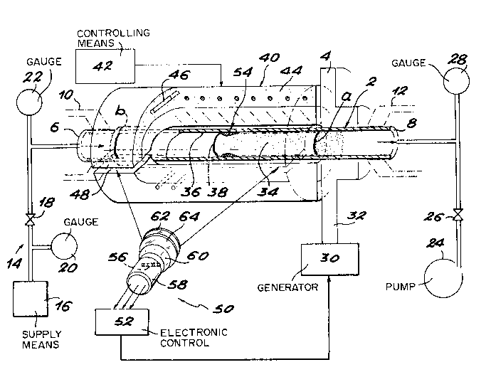
The apparatus diaylal~ ically shown in fig. 1 is intended for the
deposition of an app mpriate vitreous coating on the inner face of a
glass tube 2, e.g. of silica, with a view to obtaining a prefonm on
the basis of which will be formed the optical tubes, whose core w;ll
result from said vitreous coating.
The apparatus serves to bring out a chPm;c~l vapour phase deposition
activated by a plasma prcduced and maintained by a travelling surface
wave and to this end has an ultra-high frequency coupler 4, e.g. of
the SURF~GUIDE (~-d~.æ~) type.
The ends 6 and 8 of tube 2 are respectively hel~ by tllhll~r end
fittings or terminations 10 and 12. The ultra-high frequency ccupler
4 is located between these two end fittings, on the side of the one
carrying the reference n~n~r~l 12 in the ~ t shown in fig. 1
and thus surrcunds the tube 2 close to one of its ends. The point at
which the coupler 4 is located is advant~e~lsly autside the useful
deposition area of the vitreous coating. Moreover, coupler 4 is fixed
B 9318 C/PV
1 338054
-- 7 --
with respect to the end fittings 10 and 12. It does not move parallel
to the axis of tube 2 during the deposition of the vitreous coating
within said tube 2.
The apparatus shown in fig. 1 also comprises means 14 for injecting
through the end fitting 10 furthest frcm ooupler 4 of an appropriate
gaseous mixture, e.g. constituted by oxygen and silicon te~r~rhloride
vapour, if it is wished to obtain a pure silica ooating, or the above
mixture to which is added a dopant in the form of fluorine or a
derivative of the latter, if it is wished to obtain a fluorine-doped
silica coating. A ge~manium oxide doping would require the ~M ition
to the mixture in question of tra oe s of GeC14.
( The injection means 14 comprise means 16 able to supply the
appropriate gaseous mixture under a given pressure and supply same
to the end 6 of tube 2 via a flow regulating valve 18. Gauges 20 and
22 provide information on the pressure between means 16 and valve 18
on the one hand and between the latter and the end 6 of tube 2 on the
other.
The apparatus shown in fig. 1 also comprises means 24 for pumping the
gaseous mixture to the other end 8 of tube 2 thrcugh end fitting 12
and via a suction regulating valve 26 of the pumping means 24 (the
latter e.g. incorporating a pump such as that known under the ~dd~.~rk
R~OTS pump). A gauge 28 is also provided to give informatian on the
pressure between end 8 of tube 2 and valve 26.
The apparatus shown in fig.l also comprises a variable power microwave
generator 30 for supplying coupler 4 via a waveguide 32. Generator
30 can be externally controlled by an analog voltage varying between
O and 5 V and, in a purely indicative d non-limitative manner, can
be obtained from the company SAIREM.
When the gaseous mixture circulates within the tube 2, a plasma column
34 is formed within said tube as a result of the travelling surface
wave prcduced by coupJer 4. The vitreous coating 36 is obtained by
B 9318 C/PV
1 338054
-- 8 --
mcdifying the pawer of generator 30, which causes an alternating
variation of the length of column 34 and therefore an alternating
displacement of the end or front 38 of said column between two areas
of the interior of tube 2 and which are designated by a and b in fig. 1
and which define said useful deposition area. The distance between
areas a and b correspands to the length on which it is wished to
deposit the vitreous coating.
The internal deposition of doped or undaped silica takes place level
with the front of the plasma column, in such a way that during one
outwar~ and return travel of said front in the tube two elementary
vitreous films are deposited within the tube, all the said elementary
films constituting the vitreous coating 36. This inte m al deposition
of daped or undaped silica takes place with a excPll~nt efficiency of
approximately 100% for SiO2 and 80% for GeO2.
It is necessary to raise the interior of tube 2, where the vitreous
coating deposition takes place, to a temperature of at least approx-
imately 1000C and e.g. between 1000 and 1200C. To this end, the
apparatus shown in fig. 1 comprises an oven or furnace 40 for heating
at least the useful area of tube 2, the ends 6 and 8 of the latter
passing outside the furna oe , the latter thus extending between coupler
4 and end fitting 10. Means 42 are provided for controlling furnace
40, in such a way that the latter is at the desired temperature.
Furnace 40 comprises an envelape 44 and, within the latter, two raws
of heating elemRnts 46 extending along the furnace and positioned in
such a way that when the tube is within the furnace, it is located
between said rows of heating elcments. The latter are in the form of
regul~rly spaced bars, which are perpen~ lAr to the furna oe axis.
The envelope 44 of s~;~ furna oe is langitl~;nAlly slotted, a slit 48
being produced on the envelope 44 parallel to the fu m ace axis, which
makes it possible to observe the furna oe interior.
In the ~mhC~ nt shown in fig. 1, an alternating displacement of the
front of the plasma column 34 at a pLu~La~ ed speed, e.g. at a
B 9318 C/PV
1 338054
g
constant speed, has been sought between areas a and b. The plasma
column length L is consequently a pericdic function of the sawtooth
time t, which varies between a minimum value Lmin and a maximum value
Lmax (cf. fig. 5-A).
As will be shown hereinafter, the microwave generator 30 is appro-
priately controlled so as to supply a power P varying with the same
period as the length L as a function of the time t, between a minimum
value Pmin and a maximum value Pmax corresponding respectively to
Lmin and Lmax (cf. fig. 5-B).
In order to obtain the pL~yL~ ed speed displ~m~nt, e.g. a constant
speed, of the front of plasma column 34, the apparatus shown in fig. 1
comprises an optical sensor 50 placed outside furnace 40 and which
serves to observe at least the useful area of tube 2 when the latter
is placed inside the furnace. The apparatus shown in fig. 1 also
comprises electronic control means 52 for controlling the generator 30
as a function of signals supplied by the opti~l sensor 30, with a
view to obtaining the displacement of the front of plasma column 34
at a pLoyL~nn~d, e.g. constant spee along the axis of tube 2.
Fig. 2 ~i~gr~matically shows a longitudinal sectional view of tube 2
along axis z thereof. The gaseous mixture flowing in the tube inter-
acts with the plasma column in order to give activated species such
as Si or SiO permitting the formation of the vitreous coating. The
deposition area 54, seen in longitl~;n~l section in fig. 2, is located
at the frant of the plasma column and therefore carries out recipro-
cating movements in tube 2. The activated species in said deposition
area emit a radiation characteristic of the reaction leading to the
deposit, said radiation being in the range between the blue and the
near ultraviolet.
It should be noted that the size of the deposition area 54, in both
figs. 2 and 1, has been exaggerated in order to make said area 54
more clearly visible.
Fig. 2 also shows the variations of the intensity i of the character-
B 9318 C/PV
1 33~054
`-- -- 10 --
istic radiation, as a function of the position on the tube axis z.
The intensity i is substantially zero throughout, except in the region
corresponding to the deposition area, where said intensity i
assumes the form of a peak, which effectively reproduces, to within a
S hcmothetic transfonmation, the shape of the profile of the deposition
area seen in section. The full width at half maximum 1 of said peak
is a very gpod approximation of the real width of the deposition area
54 (to within a ~ ic transonmation).
In the embcdiment shown in fig. 1, the cQtical sensor 50 has a
10 plurality of photosensitive elements. It comprises a charge coupled
device 56 in the fonm of an array or strip and which is referred to
hereinafter as CCD array, as well as a control system or card 58 for
f said array 56. The array is fixed and placed facing slit 48, paralle
to the tube axis (which is itself parallel to the axis of furnace 40)
15 and at an apprcpriate distance frcm said slit to make it possible to
observe the useful area of the tube thrcugh an appropriate oQtics 60,
which is e.g. constituted by a camera lens.
Moreover, two filters 62, 64 are located in front of lens 60,
respectively for stopping the infrared radiation of the furnace and
20 for stoQping the visible rays of wavelengths below those of blue
radiation, so that only the characteristic radiation reaches the CCD
array.
(
Fig. 3 diayLa~l~tically shows the electronic control means 52 used
with the CCD array 56. In these ccntrol means 52, the video signal
SV supplied by card 58 associated with array 56 firstly under~oes an
analog filtering by means of a lowipass filter 66, whose cut-off
frequency is e.g. app m ximately 500 kHz, in order to eliminate f m m
the video signal the noise~ due to the resulting sampling of the CCD
array.
The thus filtered video signal is suppl;~ to the input of means 68
for detecting the maximum a~plitude of said video signal and w~ose
output is ccnnected to the input of divider means 70 able to supply
i
~ B 9318 C/PV
, ~
~ 33~054
-- 11 --
at the output a threshoid signal, whose amplitu~e is equal to half
the m2ximum amplitude of the video signal.
Card 58 supplies in electrical fonm a succession of images resulting
from the electronic scanning of the CCD array. The total of said
images constitutes the video signal. The maximum amplitude of the
video signal in practice d oes not vary between the individual images.
In addition, the relative threshold signal at each image is supplied
to a first input of a comparator 72, whose other input receives the
video signal relative to the following image. The latter is corpared
with the thresho11 signal in question in comparator 72, which supplies
at the output a TTL signal in the fonm of a rectangular pulse SG
(fig. 4) for said image.
(
The cand 58 associated with the CCD array also supplies a line
synchronization SL signal TTL (fig. 4) and a point synchronization SP
signal TTL (fig. 4). This point sync signal is in strobe form and
passes to logic state 1 whenever a photcdetector or ~point~ of the
CCD array is read. The line sync signal is a periodic signal of
period T, which is at logic state 1 throughout the image reading time.
The electronic control means shown in fig. 3 also oomprise a first
counter 74 and a second counter 76, both of which receive at the input
the signals SL, SP and SG. The first counter 74 ccunts the number of
logic states 1 of the point sync signal (number of transitions 0 to 1
or number of transitions 1 to 0 of said signal) fL~.. the time when
the line sync signal passes to logic state 1 to the time when the
signal from the comparator passes from logic state 0 to logic state 1.
The reading of the first counter 74 consequently supplies the photo-
sensitive element or photodetector number of the CCD array at which
the deposition area starts at the cansidered instant. The second
counter 76 counts the number of logic states 1 of the point sync
signal between the time when the first counter 74 stops ccunting and
the time when the signal from the comparator again passes to logic
state 0. Thus, the reading of the second counter supplies the
width at half maxImum of the deFosition area.
B 9318 C/PV
- t 338054
- 12 -
In a purely indicative and non-limitative manner, the reading of the
CCD array takes place frcm right to left in fig. 1, in such a way that
the first counter makes it possible to locate the plasma column front.
In the electronic control means shown in fig. 3, the position infor-
mation c~nc~rning the plasma column front (giving the position of the
deposition area) and the width information with respect to said
deposition area are updated at each image supplied by the CCD array
by means of card 58.
The information given by the first counter 74 or position counter
contr~ls a digital-analog converter 78, so that an analog signal is
available giving the position of the plasma column front. Converter
78 is connected to display means, such as an oscilloscope 80, so as
to be able to visually check said position of the pLasma column fr~,t.
The electronic control means shown in fig. 3 also comprises a
microprocessor 82, which reads the counters 74 and 76 and which is
associated with storage means 84 (RAM and RoM), as well as a
mi~l~cu.~uter 86 equipped with data input means 88 (e.g. a keyboard)
and output means 90, e.g. a video monitor, making it possible to
display the various infonnations.
The microprocessor uses the informations which it reads on the
counter 74 in order to produce in digital fonm a control voltage of
microwave generator 30. This digital voltage is converted into an
analog voltage signal by a digital-analog converter 92, whose output
controls generator 30.
Mi~L~cu.~uter 86 makes it possible to supply the mi~ Locessor 82
(or more precisely place in the ll~nory 84 associated therewith)
various control parameters of the apparatus ~Ccnn~;ng to fig. 1, e.g.
the positions designated by letters a and b in fig. 1.
Microprocessor 82 is controlled by a prcgram comprising interpretation
B 9318 C/PV
1 338054
- 13 -
instructions of the commands issued by the microoomputer, perfonmance
instructions for these commands and control instructions of the
microprocessor peripherals, as well as a subprogram or subroutine
constituting a closed loop control algorithm making it possible to
produce the microwave generator control voltage.
This control algorithm uses a method such as the LAGRANGE method or
method of proportional parts in order to find the zero of a function.
According to this method, the abscissa for which the function is
cancelled out is the limit of a sequence of abscissas, each term of
the sequence corresponding to the intersection of the axis of the
abscissas with the tangent to the graph of the function at the point
having for its abscissa the preceding term of the sequence.
In the apparatus shown in fig. 1, control can be either enclosed or
open loop form.
With regards the closed loop control, in the memory associated with
the microprocessor is fonmed a table of positions respectively
associated with the various positions of the fl~lt of the plasma
column in the tube, said table being defined by a ~;n;~ ~ position
Xmin and a maxim~m position Xmax and by the total number of positions
in the table, s~i~ positions being spa oed by a constant amount with
respect to one another. The micrcprocessor is also supplied with the
frequency at which said table must be traversed. For closed loop
control, the microp m cessor passes thr~ugh the position table at the
desired frequency, from Xmin to Xmax and then frcm ~max to Xmin and
then again from Xmin to Xmax and so on, which corresponds to the
sweeping of the tube by the plasma column and for each of these
successive positions X, the microprocessor c~ tes by means of the
algorithm, the control voltage of the generator making it effectively
possible to arrive at s~;~ positio,n X. More spe~ifi~Ally, the micro-
processor produces a control voltage giving a oe rtain position XR forthe plasma column front. This position is det~nm;ne~ on the basis of
the CCD array and the microprocessor ccnlores this real position XR
B 9318 C/PV
~ 333054
- 14 -
with the desir~d position X and increases or decreases the control
voltage if XR is below or abave X and so on until coincidence (with
an i~posed pr~cision) occurs between X and XR.
With regards the apen loop control, in the memory of the micropr~cessor
is also formed the aforementioned position table, as well as a voltage
table having a sequence of voltages respectively associated with the
positions of the position table. The voltage table is form~d prior
to the effective use of the apparatus shown in fig. 1 with, in said
apparatus, a tube solely serving for the control thereof. For each
position X of the position table, the micrcprocessor also seeks the
voltage to be applied to the microwave generator to obtain said
position X, by successive app mximations by means of the closed loop
control program, as has been explained hereinbefore.
When the two tables are obtained, the effective use of the apparatus
shown in fig. 1 can commence. With a tube being ready for treatment
in the apparatus, the micrcprocessor passes thr~ugh the voltage table
at the desired frequency frcm the m;n;~ voltage V~in to the maximun
voltage V~ax, then fram Vmax to V~in, then again fram Vmin to Vmax
and so on.
oscilloscope 80 makes it possible to check whether the displacement
of the plasma column front is indeed linear. It is necessary to
observe a displacement, whose time evolution is of the type shown in
fig. 5-A.
If the values XR of the real positions are different from the values
X of the desired positions, due to a drift in time of ane or other of
the parameters gove m ing the operation of the apparatus, depositian
is interrupted and the voltage table is re-formed for the same
position values which are fixed in the position table.
The c~ tion algorithm is such that it minimizes the number of
iterations making it possible to obtain the good cantrol voltage,
said number of iterations being equal to or below 4.
B 9318 C/PV
1 338054
- 15 -
Open loop control is more advantageous than closed loop control for
speed reasons. Thus, a scanning or sweeping frequency of tube 2 of
approximately 10 Hz is possible with an open loop control, whereas
with closed loop control said frequency can hardly exceed 1 Hz.
However, it should be noted that the possible scan frequencies are
dependent on the number of points of the position table and therefore
the precision desired by users for the thickness of the tube coating.
In a purely indicative and non-limitative manner, for a 50 om long
intem al coating, the position table can have 150 values.
In preferred m~nner, it is possible to obtain an apparatus controlled
by a microprocessor, which makes a periodic acquisition of the curve
of the real positions of the plasma column front as a function of
time (these positions being visible on oscilloscope 80 as in fig. 1)
and which refreshes the cantrol voltage table if this is necessary,
e.g. if the variation between the real positions and the desired
positions at the same time exceeds 5%. For starting the coating
operation, the initial voltage table can be chosen in an arbitrary
manner, bearing in mind that it must be compatible with the length of
the tube to be intPrn~lly coated.
During the mc~ tion of the microwave power, a width variation of
the deposition area is observed. Thus, the increase in the volume of
the discharge (plasma column) by a thermal effect creates an increase
in the pressure in the tube. This leads to a decrease in the
deposition area width during the displ~Pr~nt of the plasma column
front. The evolution of the pressure Pr in the tube as a function of
the length of sai~ column is shown in fig. 6, which assumes that the
apparatus according to fig. 1 is observed in such a way that the flow
of gaseous mixture takes place from right to left (unlike in the case
of figs. 1 and 2). The curve of the variations of Pr as a function
of the position Z of the plasma column front has an area PP corres-
ponding to the pressure downstream of valve 26, level with the pumping
means 24 and then increases in a substantially linear manner fram
point J (which corresponds to valve 26) and then has a level zane
and then a discontinuity at end 6 of tube 2, where the gaseous mixture
B 9318 C/PV
1 338054
is intrQduced with a pressure P1, which in the described example is
substantially equal to atmospheric pressure (approximately 10 Pa).
The pressure increases when the plasma column front moves from end 6
of tube 2 frcm a position Zl to a position Z2.
S Over a microwave power mc~ tiQn period, the pressure measured by
gauge 22 varies by a few hundred Pa, which induces deposition area
width variations of approximately 1 to 2 cm and consequently a
thickness inhcmogeneity over the length and which is estimated as
approximately 10%. In order to maintain the deposition width at a
substantially constant value, it is possible to display the latter
e.g. on a video monitor 90 and to apprQpriately act on the suction
control valve 26 of pump 24 in order to maintain the depositian area
width at the desired c~nstant value, it being necessary to increase
the opening of valve 26 when the deposition area width decreases and
to decrease the same when said width increases.
In a purely indicative an~ non-limitative manner, an example of the
use of the apparatus shown in fig. 1 is given hereinafter.
In this example, the internal and external diameters of the substrate
tube 2 are respectively 19 and 25 mm. By control, the furn æ temper-
ature is maintained at 1150C. In a preliminary phase, the gaseous
mixture is c~nstituted by pure argon with a flQw rate of 100 sccm
(standard cubic centimetres per minute) and an argon plasma is foDmed
for approximately 15 mm, which permits a very effective desorption
of the inner wall~ of the tube. The c ~ osition of the gaseous
mixture is then as follows: 800 sccm of oxygen, 200 sccm of SiC14 and
O to 30 sccm of GeC14. The pressure upstream of valve 26 is kept
c~nstant at approximately 500 Pa by means of valve 26. The microwave
power mc~ul~ting frequency is 0.2 Hz, ~ ich corresponds to a
deposition of two elementary films of the vitreous c~ating in 5
seoonds. Thus, a ~ 2400 el~ films are fonmed each
ha ~ a thickness of 0.25 micrometer, ~hidh w~e~onds to a
total deposition of 53 grams in lOO minutes.
B 9318 C/PV
1 33~54,
-- 17 --
The triangul~r reference signal stored in the memory associated with
microprocessor 82 in the form of the position table, associated with
the frequency imposed for the passage thraugh said table, permits a
controlled rn~~ tion or modification of the micrawave power between
300 and 2500 W. The resulting displacement of the deposition area is
between 20 and 70 cm with respect to the ultra-high fre~uency coupler
4, so that there is a 50 cm long deposit in tube 2, whose total
length is chosen as a consequence thereof. The precision on the
deposition area position is approximately 0.3 m~.
The pressure drop is 50 Pa, i.e. 50% over the length of the deposit,
which corresponds to a deposition area width variation of approx-
imately 596 for a width of 6 cm, i.e. 0.3 cm.
When the vitrea~s coating deposition phase is ended, the tube is
narr~ed or constricted on a gl~ss making lathe. The preform
obtained has a diameter of 18 mm and a length of 50 cm, i.e. a
kilametric capacity of 10 kilametres of fibres having an external
diameter of 125 micrameters and a core diameter of 50 micrcmeters.
Over a length greater than 75% of the total length of the fibre (10
kilametres), the variation on the core diameter is + 1 micrcmeter and
+ 3 micrameters on 90% of said 10 kilcmetres.
Fig. 7 ll;agr~nmatically illustrates other electronic control means 52
used in another apparatus according to the invention. This other
apparatus differs fram that shown in fig. 1 by the fact that the CCD
array 56 is replaced by a photosensitive linear sensor having a single
25 photosensitive element 94 associated with an electronic card 96.
El~Tent 94 has a length c~r~l~le to that of the CCD array, e.g.
30 mm and in a purely indicate and non-limitative manner can be of the
type marketed by the Sl~C car~any under refer~ce lL30. El~ment 90
is obviously parallel to slit 48 and associated with optics 60 and
30 filters 62, 64.
By means of card 96, el~nent 94 supplies an analog voltage VA
proportional to the position of the deposition area. This analog
voltage is supplied to the input of display means 97 permitting a
B 9318 C/PV
1 338G54
- 18 -
visual check of the position of the plasma column front.
This analog voltage VA is also supplied to the input of analog-digital
conversion means 98, where it is digitized and then supplied to the
input of a microprocessor 100 (homolog of the microprocessor 82 of
fig. 3), which digitally processes a control voltage of the microwave
generator 30. This digital voltage is converted into an analog
voltage signal by a digital-analog converter 101, whose output
controls generator 30.
Microprocessor 100 is associated with storage means 102 (homologs of
means 84) and a microcomputer 104 (homolog of microcoTputer 86),
which is itself associated with input 106 and output 108 means
(respectively homologs of means 88 and 90).
In a not shown variant of the apparatus described relative to fig. 1,
use is made of a mobile and not fixed optical sensor, as well as
appropriate me~.h~n;~ill means for making the s~;~ sensor perform
reciprocating movements at a constant speed along the furnace slit
and action takes place on the microwave power so that the plasma
column front constantly remains facing the mobile sensor. The latter
can comprise two rigidly integral photodetectors aligned parallel with
the slit, or a CCD array also parallel to said slit. Action takes
place on the microwave power, so that the plasma column front is
constantly between the two integral photodetectors, or between the
two end detectors of the CCD array.
B 9318 C/PV