Note: Descriptions are shown in the official language in which they were submitted.
`- 1 33821 9
PHF 87.592
Analog circuit for baseband modem.
The present invention relates to an analog circuit for a
baseband modem associated with a predefined logic circuit and
comprising members which effect electronic functions on electric
signals including, for example, filtering, amplification, putting an
analog delay into effect, comparisons, automatic equalization by means
of a non-linear arrangement.
Such an analog circuit is disclosed in the publication
"Commutation et Transmission", no. 1, 1985, which describes a Ubaseband
modem operating in duplex over two wires". The modem is mainly
constituted by a predefined logic circuit which provides the functions
which are linked to transmission, to echo cancelation and to reception
and have a plurality of passive and active bipolar circuits which
provide the analog functions including amplification, filtering,
putting an analog delay into effect, comparison and automatic
equalization. Equalization in particular is obtained by means of a non-
linear arrangement constituted by a high-pass filter whose cut-off
frequency varies automatically by the action of diodes which short-
circuit a capacitor to a certain extent. Such a modem has already a
level of integration, however to still further improve its compactness
and its reliability as well as to reduce its power consumption still
more it is desirable for several analog functions to be combined in a
CMOS integrated circuit which thus might be directly associated with
the predefined logic circuit. At any rate, the integration of these
analog functions poses obvious difficulties, more specifically as
regards the impossiblity to realize in this CMOS technology the diodes
which are necessary for the automatic equalization.
The invention has for its object to obviate this type of
difficulties and proposes means to significantly reduce the volume and
the electric power consumption and as a result thereof to improve the
reliability and the reproducibility of such a modem, whilst reducing
its cost.
To that end, the analog circuit for a baseband modem of
1 33821 9
20104-8493
the type defined in the opening paragraph, is characterized, in
that for dlrect connection to the predefined logic circuit, it is
monolithically integrated in accordance with the CMOS technique
which utilizes filters with swltched capacltors drlven by one
single clock. The frequency ls a multiple of the frequency of the
send clock of the modem, said filters adapting themselves auto-
matlcally to the data rate, the automatic equalization likewise
being obtained, and more specifically without control, by varying
and symmetrical clipping of the slgnals by means of a clrcuit
comprlslng filters havlng switched capacitors of only one type.
Such an embodlment based on swltched-capacltors filters
which are driven by one slngle clock allows a synchronous switch-
ing of the set of filters of the modem, which implies that the
fllters are no longer switched one after the other, and this also
when the modem is sub~ected to a frequency change, that the modem
operates ln the synchronous or the asynchronous mode. In addi-
tion, the use of filters havlng swltched capacitors of a single
type to reproduce the automatic equalization function is particu-
larly simple and versatlle ln contrast to the usual technlques
which employ either the stochastic gradient algorithm or the
automatic switching of several high-pass filters. The equaliza-
tlon is obtained by variable and symmetrlcal clipping of the
signals as, in accordance with the length of the line, the level
of the received signal is actually of a more or less high level
and the signal which is clipped thus to a greater or less extent,
this signal is additionally clipped in a symmetrical manner
-
1 3 3 8 2 1 9 20104-8493
relative to a fixed voltage for correct interpretation during lts
decoding.
The invention may be summarized as an analog cir-
cult assoclated wlth a predeflned loglc clrcult for forming a
modem adapted to transmlt data at a certain rate over a transmis-
slon channel, the analog circult comprlsing a clock input port
for receiving a clock signal which represents said rate, a trans-
mission section comprised of: an input port for receivlng data to
be transmitted comlng from the predefined logic circuit, at least
a transmit filter unit for flltering the data to be transmitted,
an output port for transmitting over the transmission channel the
filtered data to be transmitted, a receiving part comprised of
an input port for receiving transmitted data coming from the
transmission channel, a processing unlt comprising at least
receiving filter units for processing the transmitted data, an
output port for supplying to the predefined logic circuit pro-
cessed transmitted data, characterized, in that the analog
circuit is monolithically integrated in accordance wlth CMOS
technology, and the fllter units comprise switched capacitor
filters which include a switch control for a timing range and are
controlled by a clock signal having a frequency that is a multiple
of that applied to said clock input port.
The following description which is given by way of non-
limltative example with reference to the accompanying drawings
wlll make it better understood how the inventlon can be put lnto
effect.
1 33821 9
20104-8493
Flg. 1 shows the integrated analog circult according to
the invention and its environment, the assembly constituting a
baseband modem.
Fig. 2 shows a block diagram of the baseband modem.
Fig. 3 proposes a time diagram relative to the analog
delay function.
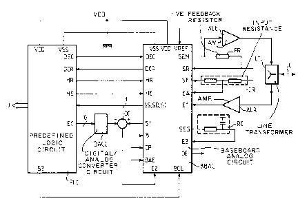
Fig. 1 the baseband analog circuit BBAC has 24
2b
1 3382 1 9
PHF 87.592 3
connection terminals connected predominantly to the predefined logic
circuit PLC. The several functions of the different connection
terminals will be explained during the description of Fig. 2.
The supply voltages are applied to the terminals VDD,
YSS and VREF and are decoupled from each other (the decoupling
capacitors are not shown in the drawing). The supply terminal VSS of
the circuits BBAC and PLC is adjusted to the 0 V potential,, whilst the
supply terminal VDD of these circuits is adjusted to a positive
potential tfor example 10 V + 5~). The potential on the supply
terminal VREF of the circuit BBAC is equal to (VDD - VSS)/2 (with, for
example, a tolerance of + 1~). Assuming Fo to be the reference
frequency which can vary from, for example, 1 kHz to 21 kHz the circuit
PLC produces a clock HR and a clock HE which are transmitted to the
circuit BBAC. The clock HR = 48 Fo is the general clock of the circuits
BBAC whilst the clock HE = 4 Fo is the sampling clock, these clocks HR
and HE being synchronized with descending edges.
Three control signals are applied to the terminals BCL,,
BHE and B of the circuits BBAC. The signal t"O"tVSS) or ~1~(VDD)] on
the terminal BCL is transmitted from the terminal B3 of PLC and allows
the control of the loop test 3 which consists in the feedback of a
fraction of the transmitted signal to the receiving side, whilst no
signal must be transmitted over the line L and no signal from the side
of the junction J must disturb the feedback. The signal ("0" or "1") at
the terminal BAE permits of positioning the logic outputs denoted SS,
SD, SI and DCR in accordance with a predetermlned configuration (which
is described in detail in the description with reference to Fig. 2).
The signals at the terminals BCL and BAE thus permit testinq of the
modem in its various functions and more specifically in its echo
cancelling function (which function is realized by the circuit PLC).
Finally, the signal ("0" or "1") at the terminal B renders a change in
the frequency range for the continuous filters possible.
Different analog signals are transmitted or transferred
towards or by the circuit BBAC and are present at the terminals listed
hereafter.
Terminal SF: transmission signal output, filtered by a
transmission filter PBEM
Terminal SR: resistor output. A resistor IR external to
1 33821 9
PHF 87.592 4
the circuit BBAC is arranged between the terminal SR and the terminal
SF and serves as the input resistance of an amplifier for matching the
level of the transmission signal AEM.
Terminal SEM: transmission signal output connected to
the output of the matching amplifier AEM. The transmission signal is
transferred towards a transmission line amplifier ALE at the side of
the line L. A negative feedback resistor FR of the amplifier AEM
external to the circuit BBAC is arranged between the terminals SEM and
SR.
Terminal EA: analog input to which a signal is applied
which when the terminal BCL has the ,,Ou value is transferred on the one
hand to the input of a filter PBRE and on the other hand towards an
input of an equalizer EGA (the filter PBRE and the equalizer EGA
will be described in detail with reference to Fig. 2). The analog
signal present at the terminal EA is a fraction of the filtered
transmission signal SR.
Terminal E1: this terminal is connected to the input of
the filter PBRE when the terminal BCL has the U1" value. It receives
the output signal from the receiving line amplifier ALR from the line
L.
Terminal E2: this terminal is connected to the input of
an analog delay line ADN (described with reference to Fig. 2). It
receives the signal coming from a differential circuit DC.
Terminal SEG: this terminal is connected to the output
of the equalizer EGA.
Terminal E3: this terminal is an input of the equalizer
EGA which in accordance with a characteristic feature of the invention
allows the shift voltage present at the output of the equalizer EGA to
be compensated for, an integrating circuit RC being connected between
the output SEG and the input E3 of the equalizer EGA.
Terminal OE: "eye" output, designated thus as it allows
the analog output signal of the equalizer EGA to be observed.
Terminal S1: filtered receiving signal output connected
to the output of the filter PBRE. This filtered receiving signal is
applied to the positive input of the differential circuit DC. Actually,
the receiving signal is received with an echo, which is caused by
impedance differences between lines and modems or by the mismatch
1 3382 1 9
PHF 87.592 5
between distant modems, which echo must be minimized or canelled. To
that end the logic circuit PLC is provided with an echo canceller which
estimates the incident echo, the output of the echo canceller EC (10
wires) then carries an estimated digital echo signal and is connected
to a digital-to-analog converter circuit DACC, which converts the
incoming logic signal into an analog estimated echo signal which is
applied to the negative input of the differential circuit DC. Thusl at
the output of the differential circuit DC a signal is available which
is the filtered receiving signal whose estimated echo has been
subtracted, this signal, as has been described already in the
foregving, is applied to the terminal E2.
Finally, logic signals are conveyed to the subsequent
terminals of the circuit BBAC.
Terminal DEC: transmission signal input. These input
data are encoded and transmitted by the logic circuit PLC and are
transferred vla the terminal DEC to the input of the transmission
filter PBEM. From this terminal the received encoded data are
outputted. These encoded data are transmitted to the output of the
equalizer EGA and are transferred vla terminal DCR to the logic
circuit PLC with the object of being decoded.
Terminal CP: this is the control terminal of the cut-off
frequency of a pre-equalizer filter PREG positioned at the input of the
equalizer EGA. This filter PREG samples the signal present at its input
at the rate 12Fo. The signal (~0~ or "1") at the terminal CP allows the
switching of the cut-off frequency fc at -3 dB, for example:
For CP = "0" fc = 0.22 Fo
for CP = U1" fc = 0.4 Fo.
The output terminals SS, SD and SI are connected to the
logic circuit PLC for transferring either the error signals utilized by
the echo canceller for cancelling the estimated echo when the terminal
BAE is at "0", or for blocking the echo canceller when the terminal BAE
is at "1~.
The terminals SS, SD and SI are connected in the circuit
BBAC to a register LAT which has for its object to store at an
ascending edge of the clock signal the value of the logic outputs of
three comparators C1, C2, C3, which cooperate with the delay line ADN
and to make these values available for use by the echo canceller of the
1 33821 9
PHF 87.592 6
circuit PLC.
In order to complete the description of the near
environment of the circuit BBAC, it is sufficient to state that the
transmission line amplifiers ALE and the receiving line amplifiers ALR,
respectively, transmit and receive the data on and from the (2-wire)
telephone line L via the line transformer LT which is thus insulated
from the transmission output SEN and the receiving input E1.
Fig. 2 shows a proposed block diagram of the baseband
modem in which the several functions of the analog circuit BBAC are
shown in detail, whilst certain functions of the logic circuit PLC
necessary for a better understanding of the mode of operation of the
circuit according to the invention will be apparent. Elements
corresponding to those in Fig. 1 have been given the same reference
numerals.
According to the basic idea of the invention, the analog
circuit is integrated in CMOS technology, using switched-capacitor
filters which are driven by a single clock whose frequency is a
multiple of the frequency of the transmission clock of the modem, said
filters adapting themselves automatically to the data rate, the
automatic equalization function also being obtained, and that without
control, by variably and symmetrically clipping signals by means of a
circuit comprising switched-capacitor filters of one single type. On
the one hand, the compatability with the logic circuit PLC, the power
consumption reduction, a better reproducibility are thus ensured whilst
the reliability, and the compactness are improved at a very low cost
and on the other hand an automatic adaptation to the data rate is
obtained by using switched-capacitor filters in CMOS technology.
Actually, these switched-capacitor filters driven by a single clock
automatically adapt themselves to the data rate, which rate can vary
from, for example, 1 kbit to 21 kbit. Moreover, the implementation of
the equalizer circuit as described hereinafter, using switched-
capacitor filters of one single type, results in a simplification in
the integration whilst still ensuring an effective adaptation without
adjustment of the slopes of the filter.
The different types of filters used in the sequel of
this description are analysed in the reference 1: "Les Filtres Actifs",
by Paul Bildstein, in Edition de la Radio.
1 3382~ 9
PHF 87.592 7
The data TD to be transmitted, present on the wire 103
(standard RS 232-V24), are scrambled in the logic circuit PLC by means
of a scrambling circuit SCR whose output is connected to an input of an
echo canceller EC and also to the input of an encoding circuit CBP to
be converted in accordance with a biphase code which is currently used
in this type of modem. Thus coded, they are transferred to the input
terminal of the transmission signal DEC of the integrated analog
circuit BBAC. The terminal DEC is connected to the input of a
-~ P~
transmission low-pass filter ~N which filters the logic signal and
recovers an analog signal which is symmetrical with respect to the
reference voltage VRF. The filter PBEN is a fourth-order low-pass
filter of the Bessel type (reference 1), whose cut-off frequency of -3
dB was in this embodiment equal to 0.92 Fo and the clock frequency HR
equal to 48 Fo. This filter PBEN is followed by a continuous filter
DCEF, commonly referred to as a post-sampling filter which renders it
possible to eliminate any spectral fold-back around the frequency 48
Fo, this filter also renders it possible to eliminate frequencies
higher than 2 Fo (HE/2), it is constituted by, for example, a second-
order cell in a Sallen-Key structure of the Butterworth type (reference
1). Taking account of the extensive working frequency range of the
circuit BBAC, it is necessary to switch the cut-off frequency of this
filter, which is obtained by means of the control signal B. Thus, the
working frequencies Fo of the circuit BBAC can, for example, be in
accordance with the control B, as follows:
B = ~0~ (VSS) 1200, 1800, 2400 3600, 4800, 6000, 7200
B = ~1u (VDD) 9600, 12000, 24400, 19200.
The output of the continuous filter DCEF is connected to
the terminal SF which itself is connected to one end of the exterior
resistor IR (see Fig. 1). The second end of the resistor IR is
connected to the terminal SR, the resistor IR is the input resistance
of the transmission signal level adapting amplifier AEM. The terminal
SR is connected to the inverting input of the amplifier AEM via an
analog interruptor B3.1 which allows the connection (or disconnection)
in accordance with the control signal BCL, of the input terminal SR to
(from) the inverting input of the amplifier AEM. The non-inverting
input of the amplifier is at the potential VREF. The output of the
amplifier AEM is connected to the terminal SEM. The feedback resistor
1 3382 1 9
PHF 87.592 8
FR is arranged between the terminal SR and the terminal SEN (see Fig.
1). An analog interruptor 83.2 allows the connection (or
disconnection), according to the control signal BCL, of the inverting
input AEM to (from) its output. The transmission signal present at the
terminal SEM is transferred to the transmission line amplifier ALE and
is thereafter transmitted over the telephone line L (2 wires) via the
line transformer LT. The amplifier AEM has for its object to provide
the interface and the adaptation of the level of the signal at the
output of the filter DCEF, it is arranged as a conventional inverter
with the aid of exterior resistors IR and FR and its gain is always
less than unity. The input signal and the output signal of AEM are
analog signals which are symmetrical relative to the voltage VREF.
In the receiving direction, the signal received from a
remote modem and passing through the telephone line L is switched in
the region of the line transformer LT to the input of the receiving
line amplifier ALR.
This received signal is a composite signal constituted
by the signal which is actually transmitted by the remote modem and an
echo signal which is basically caused by the mismatch between remote
modems and the impedance differences between lines and modems. The
output of the amplifier ALR is connected v a the input terminal E1 of
the circuit BBAC to the receiving low-pass filter PBRE which is
preceded by a continuous filter DCRF. The filter DCRF is an anti-fold
back filter by means of which the frequencies over 2 Fo can be
cancelled, and as is the filter DCEF, it is formed by, for example a
second-order cell of a Sallen-Key structure of the Butterworth type
(reference 1), and its cut-off frequency is also switchable by means of
the control signal B. The filter PBRE has for its object to filter the
analog signal received at E1, it is predominantly constituted by a
fourth-order low-pass filter of the Bessel type (reference 1) whose cut-
off frequency at -3 dB is, in this embodiment, equal to 1.25 Fo and its
clock frequency HR is equal to 48 Fo. The output of the filter PBRE is
connected to the output terminal S1. Arranged between the input
terminal E1 and the input of the continuous filter DCRF there is an
analog interruptor B3.3 which, according to the control signal BCL,
allows the connection of the input of the filter DCRF to either the
terminal E1 when the modem operates in the general mode (emission-
1 3382 1 9
PHF 87.592 9
reception), or to the input terminal EA within the frame work of aninternal test of the modem to insulate the receiving portion from the
line and to permit a portion of the transmission signal to be re-
injected (see Fig. 1). The terminal EA is also connected to a second
analog interruptor B3.4 which allows an input of the equalizer EGA
(input EB) to be connected either to the voltage REF in the general
operating mode of the modem (transmission-reception) or to the terminal
EA whitin the frame work of the internal test of the modem, to the
input EB of the equalizer, the fraction of the transmission signal
applied to the terminal EA then being re-injected.
As has already been described in the foregoing, the
filtered receiving signal (filtered by the filter PBRE), present at the
terminal S1, is beset with an echo. This echo is estimated by the echo
canceller EC, and is to be subtracted from the filtered receiving
signal. To that end, the digital estimated echo signal present at the
output (10 wires) of the echo canceller EC is converted into an analog
signal by means of the digital-to-analog converter circuit DACC. The
output signal of the circuit DACC is applied to the negative terminal
of the differential circuit DC to be split-off from the filtered
receiving signal applied to the positive terminal of the differential
circuit DC, the output of the circuit DC being connected to input E2 of
the circuit BBAC.
The input terminal E2 corresponds to the input of an
analog delay line ADN, advantageously it does not comprise more than 4
sample-and-hold circuits EB1, EB2, EB3 and EB4. The delay line ADN has
for its object to produce a delay of two sampling periods between the
input and the output of the 4 sample-and-hold circuits, which is
illustrated by Fig. 3, which shows a time diagram with respect to the
delay. This delay is necessary for a proper function of the echo
canceller EC which in known manner uses the algorithm commonly referred
to as the differential sign algorithm, the operating mode of such an
echo canceller is described in French Patent Specification no.
2,534,427. The operating principle of the line ADN is described also
with reference to Fig. 3. A sampling clock shaping circuit $~ receives
at its input, via the circuit PLC, the sampling clock HE (shown in
Fig. 3, line a ) and produces three signals HE1, HE2, HL. The signal
HE1 tFig. 3, line b ) is the sampling clock of the sample-and-hold
1 3382 1 9
PHF 87.592 10
circuits EB1 and EB3. The signal HE2 (Fig. 3, line c ) is the
sampling clock of the sample-and-hold circuits EB2 and EB4. The
sampling operation is preceded by an auto-zero period (reference EZ)
whose duration renders it possible to satisfy the settling time
(reference EST) of the circuit DACC which is subjected to a new
conversion at the falling edge of the clock HE. A data n will not be
validated until after the settling time EST calculated from the
beginning of the auto-zero period AZ, this data n will be sampled
during the remaining time SAT of the period of HE1 or HE2. The lines
d , e , f , q represent the respective periods of time during
which the data are sampled by the sample-and-hold circuits EB1, EB2,
EB3, EB4. The line h of Fig. 3 shows a clock signal HL present at an
output of the circuit CS and allows the display of the delay of two
sampling periods for a reading operation at the leading edges of the
clock signal HL.
A signal comparison arrangement cooperates with the
delay line ADN. This delay is comprised of 3 converter circuits C1, C2,
C3, and serves to supply a logic signal in dependence on the comparison
of the analog input signals. The logic signal at the output of the
converter C1 which has non-inverting inputs is representative of the
sign of the sum of the signals at the output of the sample-and-hold
circuits EB1 and EB4. To that end, the output signals of the sample-and-
hold circuits EB1 and EB4 are present at the non-inverting inputs of
the comparator C1. The logic signal at the output of the comparator C2
is representative of the sign of the difference between the signals at
the outputs of the sample-and-hold circuits EB1 and EB4. For that
purpose, the output signal of the sample-and-hold circuit EB1 is
applied to the non-inverting input of the comparator C2, whilst the
output signal from sample-and-hold circuit EB4 is applied to the
inverting input of the comparator C2. The logic signal at the output of
the comparator C3 is representative of the sign of the difference
between the output signal of the sample-and-hold circuit EB1 and the
reference voltage VREF. To that end, the output of the sample-and-hold
circuit EB1 is applied to the non-inverting input of the comparator C3
and the signal VVREF is applied to the inverting input of the
comparator C3. The outputs of the comparators C1, C2, C3 may have the
value ~0~ (VSS) for a negative sign.
- 1 3382 1 9
PHF 87.592 11
The outputs of the comparators C1, C2, C3 are connected
to the inputs of a register LAT which has for its object to store at a
rising edge of the clock HL (transmitted by the circuit CS) the logic
values of the outputs of said comparators C1, C2, C3. Actually, with
the object of simplifying the construction of the analog circuit BBAC,
the circuit BBAC comprises, to enable sampling, even at a slight
overlap, of a data n in a predetermined circuit and said data delayed
by two sampling periods (n-2), an analog delay line which is formed
from only four sample-and-hold circuits which are connected to a latch-
type register. Thanks to such a connection, it is no longer necessaryto use five sample-and-hold circuits which are indispensable to obtain
a sampling of two data delayed relative to each other by two sampling
periods, and since it is easier to obtain an integrated latch-type
register than a fifth sample-and-hold circuit, the structure of the
circuit BBAC is simplified. Thus, when ex~rining the lines _ , q
and h of Fig. 3, it will be obvious that, even with a slight overlap,
the register LAT stores at the ascending edge n of the clock HL:
*n~(n-2) at the output of the comparator C1
*n-(n-2) at the output of the comparator C2
*n-VREF at the output of the comparator C3.
The outputs of the register LAT are connected to the
outputs of the circuit BBAC. The output which is representative of the
state of the comparator C1 is connected to the terminal SS relative to
the sign of the sum of the output signals of the sample-and-hold
circuit EB1 and EB4. The output which is representative of the state of
the comparator C2 is connected to the terminal SD relative to the sign
of the difference between the output signals of the sample-and-hold
circuits EB1 and EB4. The output which is representative of the state
of the comparator C3 is connected to the terminal SI relative to the
sign of the output signal of the sample-and-hold circuit EB1 with
respect to the voltage VREF (knowing that the voltage VREF = (VVD -
VSS)/2). So as to enable the performance of the internal tests of the
modem, three interrupters are inserted between the three outputs of the
register LAT and the three output terminals SS, SD, SI. The three
interrupters are controlled by the logic terminal BAE and authorize
the connection of the outputs SS, SD and SI either, as described above,
to the three outputs of the register LAT, or to the voltage VSS (~0")
1 3382 1 9
PHF 87.592 12
for the outputs SS and SD and to the voltage VDD (~1") for the output
of SI. The three outputs SS, SD, SI are transferred (3 wires) to the
calculating member of the echo canceller EC of the circuit PLC.
In the circuit BBAC, the automatic equalizing function
is provided by the automatic equalizing circuit EGA. The circuit EGA is
designed to compensate for amplitude distorsions to which the received
signal is submitted. The line can be ranked as a low-pass filter which
significantly attenuates the high frequency components relative to the
low frequency components contained an the transferred signal. The
equalizing circuit must actually be in arrangement whose
characteristics are controlled as a function of the level of the
received signal which varies in relation with the length of the line.
The attenuated components must be amplified such that the transmitted
signal is recovered. To that end the automatic equalizing circuit is
constituted by a high-gain amplifier which is followed by a passband
equalizer filter having switched capacitors to adapt itself
automatically to the frequency of the data without adjustments of the
slopes, the cut-off frequency varying automatically, the passband
filter being formed from high-pass and low-pass filters of the same
type formed around operational amplifiers which are designed to clip
the signals in a symmetrical manner relative to a predetermined voltage
when operating in a non-linear mode.
Thus, when the line is low, the received signal is weak.
The equalizing circuit then behaves in a linear manner and corrects the
selective attenuation caused by the line. The slope of the high-pass
filters correspond to a correction of a line having average
characteristics and a maximum length. The low-pass filters cut the high
frequency (higher than the the bit frequency). When the line is short,
the received signal is at a high level. It is then amplified by the
high-gain amplifier and thereafter by the high-pass filters. It thus
rapidly reaches the clipping value. The transfer function of the
equalizer filter develops and the cut-off frequency of the high-pass
filter is modified. For a high gain (higher than or equal to 4) of the
amplifier preceding the equalizing filter, the variation in the
transfer function due to whether the signal is clipped to a greater or
less extent reliably follows the characteristic of the line. It should
be noted that the shorter the line, and consequently the lesser its
- 1 3382 1 9
PHF 87.592 13
attenuation, the stronger is the signal received and thus the transfeer
function of the equalizer filter corrects the signal relatively less.
It is important for the clipping to remain symmetrical, with respect to
a voltage which here is the reference voltage VREF = (VDD - VSS)/2,
across the overall width of the filter.
The implementation of filters of this type is subjected
to certain constraints as regards the choice of operational amplifiers
(asymmetrical supply voltage when they clip in an asymmetrical manner,
high band gain product, maximum input voltage higher than or equal to
the maximum output voltage). These operational amplifiers may, for
example, be of the type TLC 071 marketed by Texas Instruments.
The problem of providing an equalizer circuit which
operates without control is advantaqgrously solved thus.
The output signal of the sample-and-hold circuit EB1 is
applied to the automatic equalizing circuit EGA to be also sampled
there. However, the output signal of a sample-and-hold circuit is
negatively influenced (noise due to the switching action) which worsens
the signal-to-noise ratio and moreover in the present case an auto-zero
period has been imposed on the sample-and-hold circuits to allow for
the settling time of the circuit DACC, during which periods no sampling
should take place if one does not want to alter the conten of the
data. Therefore, in accordance with a preferred embodiment of the
circuit according to the invention, a pre-equalizer filter is connected
to the high-gain amplifier at the input of the automatic equalizing
circuit EGA for presampling the data and filtering the noise caused by
the switching action, thus improving the signal-to-noise ratio, the pre-
equalizer filter being in addition sampled at a frequency which is a
multiple of the frequency used for the other functions of the circuit
for a reliable recovery of the content of the data. The signal coming
from the sample-and-hold circuit EB1 is presampled in the pre-
equalizing filter PREG and the signal to be equalized is prefiltered.
The pre-equalizing filter PREG is a first-order low-pass filter
(reference 1) which uses a sampling frequency of 12 Fo, so that it is
not necessary to remove the auto-zero portion from the sample-and-hold
circuit. The cut-off frequency of -3 dBfc is switchable as a function
of an exterior command applied to the terminal CP:
1 3382 1 9
PHF 87.592 14
For CP = ~0" (VSS) then fc = 0.22 Fo.
for CP = ~1~ (VDD) then fc = 0.4 Fo.
This filter, connected to the high-gain amplifier has
three input ports. The input EA which receives the output signal from
the sample-and-hold circuit EB1 has a gain equal to 4. The input EB
which is connected to the analog interrupter B3.4 thus receives the
signal VREF when the modem functions in the normal transmission-
receiving mode and the signal present at the terminal EA when a test is
performed in the modem, this terminal EB is given a gain equal to 1/4.
Finally, the input E3 is the input which is connected to the output of
the equalizer EGA to compensate for the shift voltage present at the
output of the equalizer, this input has a gain of 2.
The output signal of the pre-equalizing filter PREG
connected to the high-gain amplifier is then applied to the input of an
equalizing low-pass filter EG comprising switched capacitors. The
signal is automatically and symmetrically clipped relative to the
voltage VREF and its amplitude is limited to, for example, 4/5 of VDD
and to 1/5 of VDD. The filter EG is constituted by four separate second-
order filters (reference 1), a high-pass filter followed by a low-pass
filter which in its turn is followed by a high-pass filter followed by
a low-pass filter, the two high-pass filters being identical and the
two low-pass filters also being identical. Finally, all these filters
are sampled at the frequency 48 Fo.
The output signal of the filter EG is filtered by
integrating circuit RCE which has a time constant which differs only
little from 1/4 Fo and is thereafter applied to the non-inverting
terminal of a comparator C4 whose inverting input is brought to the
potential VREF. The role of the comparator C4 is to convert the output
signal of the equalizer EGA from the biphase code into a binary code.
The output signal of the comparator C4 is transferred to the terminal
DCR v a a logic interrupter IE4 which is controlled by the signal
BAE, the terminal DCR then carries either a voltage VDD when the modem
effects an internal test, or the output signal from the comparator C4,
when the modem functions in the normal transmission-receiving mode. The
terminal DCR is connected to the circuit PLC where the signal is
processed by a scrambling circuit DSC at whose output the received data
signal RD is present which is to be conveyed over the wire 104
1 3382 1 9
PHF 87.592 15
(standard RS 232/V 24) and is also used to recover the clock by means
of a synchronizing circuit BS at whose output the receiving clock RCL
transferred over the wire 115 (standard RS 232/V 24) is present.
To provide an observation point between the output of
the filter EG and the comparator C4 an amplifier AO is provided which
is arranged as a tracking amplifier and consequently has a gain equal
to 1. The output of the amplifier is connected to the terminal OE which
thus represents the copy of the analog signal originating from the
equalizing circuit EGA.
Moreover, a shifting voltage may be present at the
output of the operational amplifiers used in the equalizing circuit EGA
which, multiplied by the gain, significantly disturbs the symmetry of
the clipped signal. In this case it is sufficient to compensate for
this shifting voltage. During a transmission in the baseband it is
possible to scramble the transmitted data before they are encoded, this
is the object of the scrambler SCR provided in the logic circuit PLC.
At the output of the scrambler SCR there is then a pseudo-random
digital message assembled from an equal number of zeroes ("O") and ones
("1"), when this message is examined over a sufficiently long period.
The mean value of the signal with respect to the biphase-encoded data
message is zero in this case. When this signal is received and
equalized, its mean value must remain zero. When this is no longer the
case, this indicates that a shift voltage has superposed itself on the
signal. This shift voltage must then be corrected in order to recover
the property that the mean value of the received signal must be zero.
The reason for this is that in accordance with a characteristic of the
circuit according to the invention this circuit moreover has two
connection terminals one of which is connected to the input and the
other one to the output of the automatic equalizing circuit to provide
there a connection for an integrating cell, thus forming a shift
voltage cancelling loop which imposes a zero mean value on the output
signal of the equalizing circuit. This is the object of the integrating
cell RC (see Fig. 1) which is arranged between the output SEG of the
circuit EGA and its input E3. In this manner, when the signal at the
input of the comparator C4 is not beset by any parasitic shift voltage,
the number of "O" and "1" at the output of the comparator is identical
and the shift voltage correction voltage at the output of the
PHF 87.592 16 1 3382 1 9
integrating cell RC and consequently at the input E3 is VREF = (VDD -
VSS)/2. If, on the contrary, the equalizer circuit generates a shift
voltage at the input of the comparator, an unbalance between the
numbers of ~oa and ~1" is observed at its output. The shift voltage
correcting voltage then varies in the reverse direction around the
position (VDD - VSS)/2 and forces the system to modify the shift
voltage at the input of the comparator. When balance is obtained for a
given correction voltage, it remains in existence as long as there is
coincidence between the numbers of "0" and "1". In practice a simple
resistor-capacitor circuit is sufficient to integrate the signal at the
output of the comparator. During experiments the results obtained with
switched-capacitor filters which are major sources of shift voltages
have shown that this realization is well-founded.
The modem thus obtained by connecting the integrated
analog circuit BBAC to the predefined logic circuit PLC can, as has
been described in the foregoing, operate either in the transmission-
receiving mode, or in the test mode, the operating mode being selected
by means of the control signals BCL and BAE.
The logic interrupters IE1, IE2, IE3, IE4 are controlled
by the signal applied to the terminal BAE.
If BAE = "0" (VSS), the error signals SS, SD, SI are
transferred to the echo canceller EC and the data signal ECR is
transmitted to the scrambling circuit DSC, the mode of operation is
then normal (transmission-reception), SS being the output signal of the
comparator C1, SD being the output signal of the comparator C2, SI the
output signal of the comparator C3 and DCR the output signal of the
comparator C4.
If BAE = "1" (VDD), the echo canceller is then blocked,
the terminals SS and SD being brought to the potential VSS whilst the
terminals SI and DCR are brought to the potential VDD.
The control ~CL act on the analog interruptors B3.1,
~3.2, B3.3, B3.4 and allow the selection of the loop test 3, which in
transmission equipment consists in feeding back a fraction of the
transmitted signal to the receiving side, whilst no signal must be
transmitted or received from the line or from the junction.
If BCL = "1" (VDD), the modem operates in the
transmission-receiving mode, the interrupter B3.1 connects the input SR
- 1 3382 1 9
PHF 87.592 17
to the input of the amplifier AEM, the interrupter B3.2 disconnects the
input of AEM from its output, the interruptor B3.3 connects the input
of the receiving filter PBRE to the terminal E1 and the interrupter
B3.4 connects the input EB of the equalizing circuit to the voltage
VREF.
If BCL = "O" (VSS), the modem is set to the loop
test 3 mode. The interrupter B3.1 disconnects the input SR from the
input of the amplifier AEM, the interrupter B3.2 connects the input of
AEM to its output (AEM short circuited), the interrupter B3.3 connects
the input of the filter PBRE to the input terminal EA (fraction of the
transmission signal re-injected in the input of PBRE) and the
interrupter B3.4 connects the input EB of the equalizer to the input
terminal EA.
Such a circuit connected to the predefined logic circuit
is very interesting as regards its use in a baseband modem. In addition
to its performances determined during experiments and its complete
automation, it is remarkable as regards its very high integration.