Note: Descriptions are shown in the official language in which they were submitted.
1 33~
--1--
ANAL OG -D I G I TAL CONVE RT E R
BACKGROUND
The present invention relates to an apparatus for
converting analog signals to digital signals. The invention
5 more particularly relates to circuitry for converting analog
signals to digital signals in both discrete and continuous time
doma ins .
Many different types of analog to digital converters are
known in the art. Perhaps the most common analog to digital
10 converters are the successive approximation converters, the
f lash converters, and the dual slope converters . Each have
their advantages and disadvantages. For example, the successive
approximation converters typically permit accurate conversion to
at least twelve bits, but are only of medium speed and in
15 certain embodiments require digital to analog converters having
2n capacitors, where n is the number of bits in the output
word. The flash converters are much faster than the successive
approximation converters, but require 2n 1 comparators, thus
making them costly in terms of components. Moreover, flash
20 converters currently available have an accuracy of at most nine
bits of resolution. Finally, while permitting finer resolution
and fewer components, the dual slope converters are considered
much too slow for most applications.
= ~ ~
.l ~
1 33 85 1 4
--2--
Another analog to digital converter called a
recirculating-cyclic converter or serial successive
rectification converter is known in the art. It uses a cyclic,
or stage-by-stage conversion algorithm originally employed in
high-speed, low-resolution applications, and is described in an
article by Doug Rife entitled "High Accuracy with Standard ICs:
An Elegant ADC's Forte", EDN, April 28, 1982 pp. 137-144.
Basically, according to the article, the input signal is
compared to a midpoint (ground) to see which half of the
permitted range it is in. A first bit of information is
determined thereby. The input is then rectified, multiplied by
two, and a reference voltage is subtracted therefrom through the
use of an operational amplifier and resistor network. The
voltage output VOUt, which is equal to 2 IVi I - V f
is then recirculated to the input end where a second bit is
determined by the comparator and the signal is again rectified,
multiplied by two, and decreased by the reference voltage. The
output is again recirculated, and in this manner, as many bits
o~ resolution as desired may be obtained without increasing the
component cou~t. The cycle and resolution are controlled by the
sampling timing. The Gray code output of the comparator of the
circuit is converted into binary code through the use of an
exclusive NOR gate.
_3_ l 3385 1 4
The advantage of the serial successive rectification analog
to digital converter is the reduction in the number of
components required for conversion. Indeed, with recirculation,
additional bits of resolution may be obtained without increasing
5 the numbers of components used. However, the serial successive
rectification converter is still only of medium speed, as each
additional bit of resolution requires an additional cycle of
processing .
SUMMARY OF THE INVENTION
It is therefore an object of the invention to provide a
successive rectification converter in a parallel format which
permits a fast high resolution analog to digital conversion.
It is a further object of the invention to provide a
continuous parallel successive rectification converter using
15 current steering techniques for extremely fast high resolution
analog to digital conversion.
It is yet another object of the invention to provide an
extremely ~ast high resolution analog to digital converter which
is exclusively comprised of transistors.
In accord with the objects of the invention, two
embodiments of a parallel successive rectification converter are
4 ~338514
provided. In the first embodiment, the synchronous parallel
successive rectification converter comprises:
a) a plurality of stages for performing the conversion
algorithm Vout = 2lVinl ~ Vref~ wherein Vin is
5 the voltage to the input of a particular stage, VOUt is the
voltage at the output of that stage and becomes the Vin to
the following stage, and Vref is a chosen reference voltage,
each stage comprising
i) a comparator means for comparing Vin with a second
0 reference voltage for obtaining a bit of information,
ii) a first input sampling capacitor,
iii) a second feedback capacitor, wherein the capacitance of
said first input sampling capacitor is twice that of said
feedback capacitor,
i v ) a th i rd sw i t ch capa c i t o r,
v) a switching network for permitting the charging and
discharging of said input sampling capacitor, said feedback
capacitor, and said switch capacitor according to predetermined
c lock ing,
vi) an operational amplifier having said input sampling
capacitor bridging its inverting and noninverting inputs via
said switching network, and said feedback capacitor feeding back
from the operational amplifier output to its inverting input,
wherein
said switching network is arranged to switch the connections
~ 3385 1 4
of the plates of said sampling capacitor to said operational
amplifier inputs as a function of said clocking and said
obtained bit of information to effectuate rectification of
Vin, and wherein said switching network is arranged to
5 switch the connection of said switch capacitor as a function of
said clocking from being connected to the output of said
operational amplifier to being between the source of said chosen
reference voltage and said inverting input of said operational
ampl i f ier, and
b) a plurality of shift registers, each shift register
corresponding to a particular stage and having a storage
capacity of m bits of information, where m is chosen from 0 to
n-l and is the number of said particular stage with n-l
representing the most significant bit and 0 representing the
15 least significant bit, wherein n is the number of bits output by
said analog to digital converter, wherein the output of said
shift registers provides an output word in Gray code.
In one embodiment, means for converting said Gray code
output word into a binary code output word are included.
20 Typically such means comprises exclusive OR or NOR gates.
In accord with a further aspect of the invention, the
continuous time parallel successive rectification converter for
converting an analog signal into digital form comprises:
-6- ~ 3385 1 4
a) a plurality of stages for performing the conversion
algorithm IoUt = 2 ¦ Iin ¦ ~ Iref r wherei in
the current to the input of a particular stage, IoUt is the
current at the output of that stage which becomes the Iin to
5 the next stage, and Iref is a chosen reference current, each
stage comprising
i) a current rectifier comprising a p-channel transistor and
an n-channel transistor having common gates connected to ground
and common sources connected to Iin, a first current mirror
10 with its input connected to the drain of said n-channel
transistor, and its output connected to at least the drain of
said p-channel transistor, and a second current mirror with the
drain of said p-channel transistor as an input and said IoUt
as an output,
ii) a third current mirror with said Iref as an input
and said IoUt as an output,
wherein said second current mirror of said current rectifier
has a gain of two, the analog signal converted by said apparatus
is related to the Iin current into the first stage of said
20 apparatus, and a bit of information is obtained from the
direction of the current flow of each Iin, the output bit of
each stage together forming a Gray code output word.
Preferably, the second current mirror obtains a gain of two
by arranging the transistors on the output side of said current
25 mirror to be twice the width of the corresponding transistors of
~7~ 1 33851 4
the input side of said current mirror. Also, if desired, means
for converting said Gray code output word into a binary code
output word are provided. Typically such means comprises
exclusive OR or NOR gates. It should also be recognized that
the analog signal which s to be converted into digital format is
"related" to the Iin to the frst stage of the converter in
that the analog signal may be Iin itself, or a voltage
signal analagous thereto.
Since an analog voltage is typically supplied rather than a
current, the second embodiment of the invention typically
requires the use of transconductance amplifiers to provide an
Iin and Iref. According to a further aspect of the
invention, a transconductance amplifier of the invention having
a voltage input and a current output, comprises:
a) a resistance means in series with the voltage input;
b) first and second double output current mirrors, wherein
each output of the f irst double output mirror is connected to a
corresponding output of said second double output mirror, and
the inputs are connected;
c) an operational amplifier with the inverting input
connected to ground, the noninverting input connected to said
resistance means, and the op amp output connected to the inputs
of said first and second double output mirrors,
wherein first outputs of said first and second double ouput
mirrors output are connected to said noninverting input of said
Y
1338~4
operational amplifier, and the second outputs of said first and
second double output mirrors output is connected to said
out-
A better understanding of the invention, and additional
5 advantages and objects of the invention will become apparent to
those skilled in the art upon reference to the detailed
description and the accompanying drawings.
BRIEF DESCRIPTION OF THE DRAWINGS
Figures la and Ib are respectively a block diagram o~ the
10 successive rectification algorithm of the prior art, and a
schematic of the waveforms resulting therefrom;
Figure 2 is an illustration of the Gray code decision
thresholds resulting from the successive rectif ication converter
of Figure la;
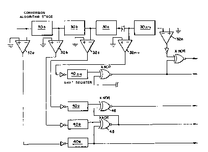
Figure 3 is a block diagram of the parallel synchronous
successive rectif ication converter of the inventi~n;
Figure ~ is a schematic of the circuitry of one stage of
the parallel synchonous successive rectification converter of
Figure 3, and the logic associated therewith;
9 1 3385 l 4
Figure 5a is a part block diagram part schematic of the
parallel continuous successive rectification converter of the
invention and the circuitry of one stage of the continuous
conver ter;
Figure 5b is a diagram defining the direction and polarity
of current flow for the continuous converter of Figure 5a;
Figure 6 is a schematic of the transconductance amplifier
used in converting voltages to currents for use with the
continuous analog-digital converter of Figure 5a.
DETAILED DESCRIPTIO~ OF THE PREFERRED EMBODIMENTS
Turning to Figure la, a block diagram of the successive
rectification converter algorithm of the art is shown. As seen
at 12, a sampled analog signal Vin 14a having a voltage
between -V f and Vr f is compared to another reference
voltage (ground~ by comparator 15a. A first bit of information
as to whether the sampled voltage is positive or negative is
obtained thereby. The input voltage is then rectified and
amplified by a factor of two at rectifier-amplifier 17a, and
Vref is subtracted from the resulting voltage at summing
j unction 20a to obtain VOUt 24a . VOUt 24a may be
considered to be the input voltage 14b to the second stage of
1 3385 1 4
--10--
i
the analog-digital converter. The process may then be repeated,
with a second bit of information being obtained by comparing the
new Vin 14b to ground at comparator 15b. The new input
voltage 14b is then rectified and amplified by a factor of two
5 at rectifier-amplifier 17b, and Vref is subtracted from the
resulting voltage at adding junction 20b to obtain VOUt 24b.
The same process may be repeated as many times as desired in
multiple identical stages to obtain as many bits of resolution
as is required. Alternatively, the VOUt of the first stage
10 may be recirculated back as a new input to the first stage
provided proper clocking and switching are utilized.
Those skilled in the art will appreciate that the
amplification of the signal accomplished by the successive
rectification converter avoids the problems of the successive
15 approximation converters and flash converters of the art where
signal amplitudes are attenuated and descend to the millivolt or
microvolt region depending on the amount of resolution desired.
Indeed, the effect of the rectification, amplification and
subtraction is to fold the input signal about zero volts as seen
20 at 25a in Figure lb. The repeated folding of the input signal
at 2~a, 25b,... divides the input signal into 2n segments,
where n is the number of bits of resolution desired, and n-l is
the amount of stages required. Any input may then be
represented in a Gray code according to the region in which it
25 falls. For example, as seen in Figure 2 a decision threshold
Y
-11- 13385~4
chart may be arranged where the shaded region for each
comparator signifies a negative value while the un6haded region
designates a positive value. The shading for each comparator
may respectively be taken from signals 25a, 25b,... of Figure
5 lb. With four bits of resolution, an input voltage may be said
to lie in one of sixteen unique segments. Each segment may then
be represented by reading the threshold chart and assigning a
zero to shaded regions and a one to unshaded regions. It will
be recognized that a Gray code output results, with the lowest
input coded as 0111, the next input coded as 0110, etc. The
most positive value would be coded as 1111.
The Gray code output of Figure 2 can be ef fec~ently
converted into a binary output if required. One method of
converting the code would be to use a look-up chart (e.g. a
15 ROM). Another approach requires that a word of code be read
from the most significant bit to the least significant bit. If
the inspected bit is a one, then the next bit remains unchanged.
If the inspected bit is a zero, then the next bit is inverted.
Thus, it will be seen that the lowest input, which was coded as
0111 in the Gray code, will be converted to 0000. The first "1"
is inverted by the zero in front of it, leaving 0011. The
resulting zero of the second bit then inverts the third bit's
"1" into a zero, which in turn inverts the last bit, leaving
0000. Likewise, the second lowest value will become 0001, as
the two "l's" will be inverted into zeroes, and the zero in the
y
_ _ _ _ _ . _ . . _ ~ .. . . .
1 33 85 ~ 4
lsb will be inverted into a "1". Those skilled in the art will
appreciate that such an operation may be realised by taking the
exclusive NOR of the current bit and its predecessor to form the
new current bit.
An implementation of the successive rectification converter
algorithm in a parallel synchronous form according to the
invention is seen in block diagram form in Figure 3. One stage
30a for performing the conversion algorithm VOUt =
2 lVin I ~ Vref, is shown in Figure 4 and comprises a
comparator 32, op amp 35, an input sampling capacitor C1, a
feedback capacitor C2, a switch capacitor C3, switches Sl
through S10, logic circuitry 36, and clock generator 38. As
will be described in more detail below, a first bit of
information is obtained by comparing the voltage Vin to
ground. Then, when switches S5 and S6 are opened, input
sampling capacitor Cl is charged up to Vin. When the charge
of Cl is released by C1 through a rectifier comprised of
switches S1 through S4, the feedback capacitor C2 is charged to
twice the absolute value of Vin, because the capacitance of
20 Cl is arranged to be twice that of C2 . S imultaneously,
capacitor C3 is connected to the inverting op amp side of
capacitor C2 and because capacltor C3 sees a voltage Vref,
the voltage over C2 is decreased by the value of Vref when
C2 has has a capacitance equal to C3. In this manner, a
25 VOut equal to 2 IV. - V
ln I ref lS provided . The
1 3 3 85 1 4
--13--
voltage output of the first stage 30a becomes the voltage input
into stage 30b where identical circuitry performs the identical
function. The logic for controlling the switches of stage 30a
is seen as gates Gl and G2, flip-flop sl and clock circuitry 38.
5 Those skilled in the art will recognize that only one clock
generator is required to control as many algorithm per~orming
stages 30a, 30b, 30c.. . as are being utilized. However, each
stage reguires the equivalent of gates Gl and G2 and flip-flop
Bl .
According to the parallel synchronous embodiment, the
information bit outputs of the comparators 32 of each stage are
inverted (as the inputs were originally sent to the inverting
input) and sent to shift registers 40a, 40b..., as seen in
Figure 3. The storage capacity o~ shift register 40a is
15 preferably arranged to be m bits of information, where m equals
n-l for the most signif icant bit and 0 for the least signif icant
bit, and where n is the number of bits of resolution being
utilized, and n-l is the number of stages utilized. Thus, it
will be understood that no shift register is required for the
20 information determined by a last comparator located at the
output of the last stage, as the shift register would have zero
storage capacity.
In operation, a sample of an analog voltage signal having
voltage Vin is provided to the negative input of comparator
.... _ .. _ .. ,
-14- 1 3385 1 4
32 and compared to ground. Switches Sll-S17 and capacitor C4
are provided in eonjunction with comparator 32 to eliminate
offset problems and to take the criticality out of the design of
the comparator 32. A first bit of information is obtained from
5 comparator 32 and sent to shift register 40a and to logic
circuitry 36, and in partieular to the D input of flip-flop Bl.
When non-overlapping eloek generator 38, which is comprised of a
clock input, a negatively edge triggered binary eounter 42, a
positively edge triggered flip-flop B2, NOR gate G3, NAND gate
10 G4 and invertors G5 and G6, provides an even phase, switehes S5
and S6 are elosed and capacitor Cl is eharged up to a voltage of
Vin as switehes Sl - s4 are all open.
On the negative edge of the even phase, the not even phase
input into Bl goes high, eausing whatever information is at D to
15 be transferred to not Q. I~ Vin is greater than ground, the
output from comparator 32 is low as is the not Q output of Bl.
Conversely, the Q output of Bl goes high eausing NOR gate G2 to
be low, thereby leaving switehes Sl and 54 open. Meanwhile,
with the not Q output of Bl being low, when the odd phase starts
20 (clock generator 38 is non-overlapping), the not odd phase goes
low, causing NOF~ gate Gl high and resulting in the elosing of
switches 52 and 53. If Vin was negative, Gl would go low
and G2 would go high, thereby causing switehes 51 and s4 to
close and switches 52 and 53 to open. Those skilled in the art
25 will appreciate that this eombination of switehes and logic acts
Y
-15- 1 33 85 1 4
to rectify the Vin signal by switching the connection of the
plates of capacitor Cl to the op amp 35, and thereby causing a
-Vin voltage to appear at the inverting input of op amp 35.
As stated above, when switches Sl and S4 or S2 and S3
5 close, the voltage -Vin is seen at the inverting input of op
amp 35. In response, the op amp immediately causes its output
voltage to swing high, thereby pulling a current. In this
manner, the charge stored on Cl is transferred to capacitor C2,
ultimately leaving the potential across C1 at zero and thereby
10 bringing the inverting input of op amp 35 to ground. When the
voltage at the inverting input of op amp 35 reaches ground, the
system is in equilibrium. Because Cl is arranged to have a
capacitance twice that of C2, in equilibrium, the voltage at the
output of op amp 35 and across C2 becomes twice that of the
15 former voltage across Cl (i.e. 2IVinl). Thus, the
arrangement of providing an operational amplifier with an input
sampling capacitor Cl bridging (via switching network Sl-S4) its
inverting and noninverting inputs, and a feedback capacitor C2
feeding back from the operational amplifier output to its
20 inverting input, permits the rectified Vin signal to be
amplified by a factor of two at the output of op amp 35.
When the odd phase is high, not only does the charge on
capacitor Cl get transferred to C2, but switches S7 and S9 close
causing the final aspect of the successive rectification
/~ ~ 3385 1 4
algorithm to be performed simultaneously. When switch S9 is
closed, the voltage of Vref appears at one plate of
capacitor C3 thereby causing the other to charge to Vref.
In response to the non-zero voltage (Vref) appearing at its
5 inverting input, the voltage output of op amp 35 swings low
causing current to flow until an equilibrium is reached. In
essence, when the capacitance of C2 and C3 are equal, the
equilibrium due to Vref is reached when the voltage at the
output of op amp 35 and across C2 is decreased by Vref. The
lO decrease of voltage across capacitor C2 causes the inverting
input of operational amplifier 35 to ground. Thus, the voltage
at the output of op amp 35 becomes 2 ¦Vin ¦ - Vref . This
output voltage is then fed into stage 30b as the input voltage
of that stage, where it is tested by a comparator to see whether
15 it is a positive or negative voltage. As aforedescribed, the
determination of the comparator provides another bit of
information which is sent to shift register 40b. The voltage
input is then processed by identical circuitry and fed
successively into additional identical 6tages. In order to
20 provide n bits of resolution, the analog signal Vin must be
processed by n - 1 stages, and a comparator 40n must be located
at the output of the last stage.
Those skilled in the art will appreciate that the
arrangement of C2 and C3 and switches S7-S10 also provide a
25 voltage cancelling function to permit the performance of the
-17- 1 3385 1 4
algorithm. Thus, after C2 and C3 have been charged to VOUt
and Vref respectively, and a new cycle starts, C3 i8 charged
to VOUt during the even phase because switches S8 and S10
are closed. Since VO t refers to the voltage of the
5 previous cycle, it may also be designated as VOld. When the
new odd phase starts, C2 is actually charged to 2¦Vin¦ +
VOld - (Vref + VOld). It will be appreciated that
the old voltages across the capacitors cancel out to provide the
des i r ed resu 1 t .
Those skilled in the art will also understand that
according to the best mode, the switches Sl-S17, gates Gl and
G2, and flip-flop Bl of each successive stage are triggered by
opposite phases.- Thus, in stage 30b, switches S5 and S6 are
preferably closed during the odd phase when a VOUt is being
15 determined and provided by stage 30a, thus permitting the
sampling capacitor Cl of stage 30b to charge to the VOUt
voltage of stage 30a. Likewise, gates Gl and G2 which control
switches sl-s4 would be triggered by the start of the even phase
(not even phase going low). Also switches S7 and S9 would close
20 during the even phase, while switches S8 and S10 would close
dur ing the odd phase .
As a~oredescribed, the shift registers 40 associated with
the various stages 30, have a storage capacity of m bits of
information with m ranging from n-l to ~. Thus, the shift
- 1 33~5 1 4
--18--
register 40a associated with stage 30a, which is actually
located before the processing circuitry, has a storage capacity
of n - 1 (or seven) bits, while the shift register 40b
associated with stage 30b has a storage capacity of n - 2 (six)
5 bits of information. In an eight bit converter, the sixth stage
would have a shift register storage capacity of two bits of
information, and the last stage (m = 1) would have a shift
register with a single bit capacity. The output of the seventh
stage would then be fed to a comparator without a concomitant
lO stage and without a shift register. This last comparator would
provide the least signif icant bit of information .
It should be appreciated that each stage 30 will take an
identical length o~ time to provide a voltage output equal to
twice the absolute value of the input voltage minus the
15 reference voltage. Thus, while the second stage 30b is
processing the input voltage provided by the first stage to
provide an output voltage, the first stage 30a will be
processing a second sample of the analog input. Indeed, those
skilled in the art will recognize that if stage 30a, which
20 (before processing) provides the most significant bit of
information (the "t = 0 bit") is said to provide the same at
time t = 0, the second stage, 30b will compare the output of
stage 30a and provi8e a second bit of information at time t = l.
The last stage processes the t = 0 sample and sends it to a
25 comparator at time t = 7, at which time the first stage is
....... _ . . _ . . .. _ . _ . ~ . _.. . .. . .. _ . . _ . .. _ _ . .. _ .
-19- 1 3385 1 4
sampling and providing its eighth bit of information. Because
shift register 40a has a storage capacity of only seven bits,
the t = 0 sample bit of information is output by shift register
40a at the identical time (t = 7) that the last stage outputs
5 its "t = 0 bit" of information. Likewise, all of the
intermediate shift registers 40b, 40c... simultaneously output
their t = 0 bit of information. Thus, an eight-bit digital Gray
code word representing a sample of an analog signal is provided
by the shift registers 40a, 40b... for each time period. In
lO other words, after seven time periods, the invention permits the
production of an eight bit word of information approximately
eight times as fast as the recirculating or serial successive
rectification converters of the prior art. Of course, sixteen
bit words could be produced sixteen times as fast. It should be
15 understood that it is not intended that the invention be limited
to eight bit and sixteen bit situations, but rather that the
invention encompasses parallel synchronous successive
rectification regardless of word length.
Those skilled in the art will appreciate that the Gray code
20 words output by the parallel synchronous successive
rectification embodiment of the invention may be converted to
binary code according to the techniques discussed with regard to
Figures 1 and 2 herein. Preferably the conversion is
accomplished through the use of exclusive ~OR gates as seen in
25 Figure 3. Thus, the bit output by shift register 40a (the
-20- 1 3385 1 4
"msb") i8 taken intact, and is also used as an input into
exclusive NOR gate 45. The other input into gate 45 is the bit
output by shift register 40b. If the msb is a zero, the bit
output by shift register 40b is inverted by gate 45. If the msb
5 is a one, the bit output by shift register 40b remains intact.
Regardless, the output of gate 45 provides the second bit of the
binary word and an input into exclusive NOR gate 46. Again, the
output of the previous shift register (in this case 40b)
determines whether the bit being output by shift register 40c is
lO to be inverted or not, and the output of gate 46 is used as the
third bit of the binary word and an input into yet another
exclusive NOR gate. Those skilled in the art will appreciate
that n-l exclusive NOR gates are used to convert the Gray code
output of the invention into a binary output word of n bits.
Turning to Figure 5a, the continuous time embodiment of the
successive rectification ~-D converter is shown implemented with
MOSFETs. Figure 5a should be understood with reference to
Figure 5b which defines the direction and polarity of current
flow. Thus, a current flow out of the input will be considered
20 to be a positive current (providing a negative voltage), while a
current flow into the output will also be considered a positive
current .
P,s seen in Figure 5a, the continuous time embodiment
re uires an in ut current I.
q P ln and a reference current
1~ .
-21- 1 338~ 1 4
Iref, and transconductance amplifiers for converting input
and reference voltages into currents are typically utilized. A
particular transconductance amplifier for accomplishing the same
will be described more fully hereinafter.
As with the parallel synchronous time embodiment, the
continuous time embodiment implements the successive
rectification algorithm of the art, except that voltages are
changed into currents. Thus, a plurality of stages 60a,
60b,...for performing the conversion algorithm IoUt =
lO 2¦Iin~ - Iref are provided wherein Ii 62 is the
current at the input of a particular stage, Io t 64 is the
current at the output of that stage which becomes the Iin f
the next stage, and Iref 66 is a chosen reference current.
In order to provide a rectified input current, a current
15 rectifier 68 is provided and essentially comprises: a
complimentary transistor pair having an n-channel FET Ml and a
p-channel FET M2 with common gates connected to ground, and
common sources connected to the source of Ii 62; a first
current mirror 70 having p-channel FETs M6, M15, M5 and M7, with
20 the input connected to the drain of said p-channel FET Ml, and
the output connected to at least the drain of said n-channel FET
M2; and a second FET current mirror 75 having n-channel FETS
M16, M4, M8, and M9, with the drain of p-channel FET M2 as the
inputr and current flowing from Iout 64 as the output
-22- 1 3 3 8 5 1 4
Those skilled in the art will appreciate that this arrangement
provides an offset-free current rectifier. Those s~cilled in the
art will also appreciate that a current rectifier is also
defined by only the complimentary transistor pair Ml and M2 and
5 the current mirror 70 arranged as aforedescribed. However, the
second current mirror 75 is useful in permitting the rectifier
to inter~ace with additional circuitry.
The amplification of the Iin current by a factor of two
is accomplished in the second FET current mirror 75 by having
10 the widths of the mirror FETs M8 and M9 being twice the widths
of their corresponding FETs M16 and M4.
A third FET current mirror 80 comprising p-channel EETs
Mll, M12, M13, and M14 is used to complete the algorithm by
subtracting the Iref current 66 from Iout 64. Thus,
15 Iref 66 ~which may be derived by processing Vref with a
transconductance ampifier) serves as the current mirror input
and is connected to the drain of FET M14. In turn a mirror
cbrrent is provided at the drain of FET Mll, and that output is
connected to IoUt 64. Nith the current rectifier,
20 amplifier, and subtractor so arranged, the input current is
processed and leaves stage 60a according to the algorithm
t = 2 ~ - I f . As with the parallel
synchronous embodiment of the invention, the output of one stage
becomes the input to the successive stage.
--23--
1 3385 l 4
In operation, a first bit of information is derived from
the direction of the flow of current Iin 62. If current is
flowing out (positive flow) of the circuitry toward the current
source (transconductance amplifier), the provided voltage may be
5 assumed to be negative as the gate of Ml is at ground. Current
flowing into stage 60a (negative flow) may be considered
evidence of a positive voltage. With the sources of FETs M6,
M5, and M12 at a positive supply potential, and the sources of
FETs M4 and M9 at a negative supply potential, if the current is
lO flowing negatively at stage 60a, it must necessarily follow a
path through FETs M2, M16, and M4, as FET Ml will not allow
current to flow through it in that direction. As a result of
that flow, FETs M8 and M9, which complete the second current
mirror 75, provide a twin current which mirrors FETs M16 and M4.
15 However, because FETs M8 and M9 are arranged to have twice the
widths of FETs M16 and M4, the current flowing through FETs M8
and M9 is twice that of the current Iin flowing through FETs
M16 and M4.
If the current is flowing positively (out of) at stage 60a,
20 the current must necessarily be collling from FETs M6, M15, and
Ml, as FET M2 will not permit current to flow through it in such
a direction. As a result of the current flowing through FETs M6
and M15, an equal current flows through FETs M5 and M7, as FETs
M5 and M7 complete the first current mirror 70. Current leaving
_ _ _
-24- 1 3385 1 4
the drain of FET M7 continues through the drain of EET M16
because of the gate-drain short of FET M16 and then continues
through FET M4. The flow of current through FETs M16 and M4
cause a flow through FETs M8 and M9 of twice the Iin
5 current, as previously described, because FETs M8 and M9
complete second current mirror 75 and because FETs M8 and M9 are
twice the width of FETs M16 and M4. Thus, it is seen that the
combination of the complimentary transistor pair Ml and M2 with
f irst current mirror 70 and second current mirror 75 acts to
lO rectify the current signal, as the current magnitude dictated by
Iin will always flow in the same direction through FETs M8
and M9. Because the current is "supplied" by Iout, the
current due to 2IVinl will always flow positively from the
input of stage 60b, and will always be positively rectified.
15 It is also seen that the input current signal may be amplified
by a factor of two by causing the transistors on the mirror side
of the second current mirror 75 to be twice the width of the
corresponding transistors on the input side.
The operation of the final aspect of the successive
20 rectif ication algorithm is seen by referring to Iref 66 and
third current mirror 80. ;3y choosing Iref to be a current
in a defined direction, the Iref current is forced to flow
down through FETs M~3 and M14. The current flow through FETs
M13 and M14 causes an identical current to flow through FETs M12
25 and M11, the mirror FETs of current mirror 80. Thus, current
y
-25- 1 3385 1 4
Iref, by definition, flows negatively at IoUt, in the
opposite direction of the current (2 l Iin I ) flowing through
FETs M~ and M9, and completes the operation. As the IoUt of
stage 60a is the Iin of stage 60b, a second bit of
5 information may be determined by determining the direction of
the flow of current at the input to stage 60b. Indeed, as
aforementioned, if the current is flowing out of stage 60b
(positive flow), the voltage will be measured as a negative
voltage as the gate of the Ml FET of stage 60b is at ground.
lO Conversely, current flowing into stage 60b will be provide a
positive voltage measurement.
As with the parallel synchronous embodiment of the
invention, the output of the stages provides information in a
Gray code. Again, if desired, the Gray code may be converted
15 into binary information by processing it through exclusive NOF~
gates. Indeed, it should be understood that because the
algorithm utilized remains constant, the resulting Gray codes of
the invention embodiments are identical.
Those skilled in the art will appreciate that the
20 continuous parallel successive rectif ication A-D converter is
extremely fast in providing as many bits of resolution as is
required because it uses current steering techniques rather than
capacitors. Indeed, it is therefore aptly described as a
continuous converter as no switches are required ~or timing. It
_ _ _ _ _ _ _ _ _ _ _ _ _ _ _ _ _ _ _ . . _ .
-26- 1 3385 1 4
is also extremely energy efficient as the FETs of the embodiment
use very little power. Thus, a continuous time parallel
successive rectification A-D converter modelled according to the
teachings of the invention was able to provide six bits of
5 resolution in 290 nanoseconds, and twelve bits of resolution in
580 nanoseconds. The wattage per stage was approximately .5
milliwatts. However, the transconductance amplifiers used to
convert the reference and sampled voltages into currents
utilized 192 milliwatts. It should be recognized that such an
lO overall performance permits the realization of the invention in
microchips and integrated circuits, and permits the employment
of the invention in a wide range of devices.
Turning to Figure 6, the preferred transconductance
amplifier used with the continuous time successive rectification
15 A-D converter invention is seen and generally comprises an op
amp 80, a resistor 82, and two double output current mirrors 84
and 86. The resistor 82 is connected in series between the
voltage input Vin 88 and the noninverting input of the
operational amplifier 80. The inverting input of the op amp 80
20 is connected to ground. The output of the op amp 80 is
connected to and acts as the input of the double output current
mirrors 84 and 86 . A f irst double output current mirror
comprises p-channel FETs Tl, T2, T3, T4, T5, and T6, with FETs
Tl, T3, and T5 having connected or common gates and connected or
25 common sources, and FETs T2, T4, and T6 having connected or
1 3385 1 4
27
common gates. FETs Tl, T4 and T5 are shorted with their gates
being connected to their drains. The drains of FETs Tl, T3, an
T5 are respectively connected to the sources of FETs T2, T4, and
T6. The sources of FETs T2 and T6 (the outputs) are
5 respectively connected to the noninverting input o~ op amp 80
and a node from which IoUt 90 is taken, with the source of
FET T4 (the input) connected to the output of omp amp 80.
Second double output current mirror 86 comprises n-channel
FETs T7, T8, T9, T10, Tll, and T12. FETs T8, T10, and T12 have
lO connected or common sources and gate~, with FETs T8 and T12
being shorted by having their gates conected to their drains.
The drains of FETs T8, T10, and T12 are respectively connected
to the sources of FETs T7, T9, and Tll which have common or
connected gates. FET T9 is shorted with its gate being
15 connected to its drain. The drains of FETs T7, T9, and Tll are
respectively connected to the drains of FETs T2, T4, and T6.
In operation, the input voltage 88 causes a current to flow
through resistance means 82, and also causes a voltage to appear
at the noninverting input to amplifier 80. For purposes of
20 example, if the input voltage was of positive polarity, the
response of the op amp 80 would be to increase the output
voltage of the op amp 80. A higher voltage at the ouput would
cause an increased current flow in FETs T9 and T10, and a
decreased flow in FETs T3 and T4 if a constant voltage
y
-28- 1 3385 1 4
difference is maintained between the sources of FETs T1, T3, and
T5, and the sources of FETs T8, T10, and T12. Because FET T9 is
the input into the double output current mirror 86, the current
flow through FETs T9 and T10 will cause twin flows to occur both
in FETs T7 and T8, and T11 and T12. The exact ratio oF the flow
will depend on the relative channel widths of FETs T10, T8 and
T12. As shown in Figure 6, the ratio of current flow in FETs
T8, T10, and T12 will be m:l:n. Likewise, because FET T4 is
the input to double output current mirror 84, the current flow
through FETs T3 and T4 will cause twin flows to occur both in
FETs Tl and T2, and T5 and T6. Because the ratio of the widths
of Tl, T3, and T5 is arranged to correspond to the ratio of the
widths of T8, T10, and T12, the ratio of the current flow
through FETs Tl, T3, and T5 is m:l:n.
Those skilled in the art will understand that the resulting
current IoUt 90 from the transconductance amplifier as
described will be the difference of the current flowing into
FETs T6 and Tll. The total current IoUt according to the
invention is equal to Vin (n/mR), where the transconductance
gm is def ined as n/mR.
There has been described and illustrated herein apparatus
for converting analog signals into digital signals, and an
apparatus for converting a voltage into a corresponding current.
While particular embodiments of the invention have been
Y
-29- 1 338~ 1 4
described, it is not intended that the invention be limited
thereby, as it is intended that the invention be broad in scope
and that the specifications be read likewise. For example,
while the continuous parallel successive rectification converter
5 was described as using current mirrors each having four
transistors, different current mirrors using two, three, or
other amounts of transistors could be effectively used.
Likewise, while particular logic circuitry was supplied for the
parallel synchronous converter embodiment, different logic
10 providing similar results could be easily constructed. Further,
while a particular transconductance amplifier was described for
use with the continuous converter embodiment, other
transconductance amplifiers known in the art may also be used.
It should a~so be recognized that the converters and
15 amplifier of the invention may be realized in many different
forms. For example, discrete components may be used for each of
the described devices. Or, if desired, the components may be
partially or fully integrated into an integrated circuit.
Finally, if desired, equivalent componentry may be substituted
20 with only minor resulting changes in the designs and results.
Thus, for example, the MOSFETs used and described could be
replaced by bipolar transistors and resistors, if desired, and
it is intended that the invention encompass such minor changes.
Indeed, it is intended that the terminology relating to the
25 transistors be used in a broad sense, with "source" being
~ ..
_3~- 1 33851 4
generic for a source or emitter, "gate" being generic for a gate
or base, etc. Therefore, it will be apparent to those skilled
in the art that other changes and modifications may be made to
the invention as described in the specification without
5 departing from the spirit and scope of the invention as claimed.